Abstract
AlxGa1−xN nanowires are the key materials for next-generation ultraviolet (UV) detectors. However, such devices have a low quantum efficiency caused by the introduction of defects and impurities throughout the preparation process of nanowires. Herein, the effects of different interstitial defects and vacancy defects on the electronic structure of Al0.5Ga0.5N nanowires are investigated using density functional theory calculations. Our results successfully discovered that only the formation of an N interstitial defect is thermally stable. In addition, the introduction of different defects makes the different nanowires exhibit n-type or p-type characteristics. Additionally, different defects lead to a decrease in the conduction band minimum in band structures, which is the major cause for the decrease in work function and increase in electron affinity of Al0.5Ga0.5N nanowires. What is more, the calculation of the partial density of states also proved that the interstitial defects contribute to a re-hybridization of local electron orbitals and then cause more significant movement of the electron density. Our investigations provide theoretical guidance for the pursuit of higher-quantum-efficiency ultraviolet (UV) detectors.
1. Introduction
In recent years, III–V semiconductor nanowires have been intensively selected in the realm of optoelectronic devices such as solar cells, photodetectors, lasers, and other nanoscale devices [1,2,3], owing to their fascinating characteristics [4,5,6,7]. Furthermore, the AlxGa1−xN nanowire photocathode has become the most promising candidates for ultraviolet (UV) detectors due to its adjustable band gap, high temperature resistance, and high sensitivity. However, the defects and impurities throughout the growth and preparation process are the main factors affecting the quantum efficiency of photocathodes [8,9,10,11,12]. Additionally, numerous experiments have detected the defects and impurities on the surface of nanowires [13,14,15,16]. Hemesath et al. investigated the incorporation of Au atoms in Si nanowire and proposed new criteria for the stability of planar defects [13]. Biswas et al. discovered that metal impurities in germanium nanowires could substantially alter their electronic and optical properties [14]. Chen et al. studied the incorporation of metal atoms into silicon nanowires and proposed a dimer-atom-insertion kinetic model to explain the impurity incorporation into nanowires [15]. Álvarez et al. found that in InAs nanowires, the surface properties are intimately related to the formation and reaction of surface point defects [16]. However, the experimental studies cannot correctly quantify the variations in nanostructure around the defects and impurities throughout the material growth process. Fortunately, the first-principles calculation method based on density functional theory (DFT) has emerged as an effective means to solve this problem [17,18,19]. A large number of studies have been carried out to analyze the effect of defects on the performance of nanowires by first-principles calculations on the basis of no experiments. For example, Yang et al. found through calculations that the AsGa point defect is highly stable in the As-rich condition, regardless of whether the GaAs nanowires are exposed or hydrogen-passive. At the same time, the existence of AsGa point defects inhibits the p-type doping process of GaAs nanowires [20]. Using first principles, Liao et al. found that CN point defects are more likely to exist on the surface of GaN NWs, and when the defect is closer to the outer side, the effect on the top of the valence band is greater [21]. Kong et al. analyzed first-principles calculations to demonstrate that N vacancy is more likely to exist at the surface of the GaN nanowires and deteriorate the stability [22]. Liu et al. posited that Zn-doped GaAs nanowire suffer more significant surface defects under the same growth conditions due to lower formation energy [23]. Lu et al. explored the optoelectronic properties of native point on GaN nanowires and found that NGa substitutional defects are the surface defects with the lowest formation energy [24]. Therefore, it is of great significance to study the effect of defects on the properties of nanowires by first-principles calculations. Nevertheless, there are few investigations into the defects and impurities of the Al0.5Ga0.5N nanowire surface. Therefore, in this study, according to the first-principles calculation method, we investigated the impact of surface defects on the electronic characteristics of Al0.5Ga0.5N nanowires.
Herein, interstitial defects and vacancy defects are considered in this study. In addition, in order to maintain the Al composition, only Ga atom and N atom vacancy defects are discussed in this article. The formation energy, work function, electron affinity, geometric structure, Mulliken charge distribution, energy band, and partial density of states are computed and discussed. This study not only explains the physical mechanism of the effect of defects on the Al0.5Ga0.5N nanowire surface but also provide significant guidance for the preparation of high-performance AlxGa1™xN nanowire-based photocathodes.
2. Calculation Models and Method
All calculations were operated in the Vienna ab initio Simulation Package (VASP) program [25,26]. The Heyd–Scuseria–Ernzerhof (HSE06) functional was implemented to handle the electronic exchanges [27,28]. Following a thorough convergence test, the high energy cut-off was determined to be 400 eV, the thickness of the surrounding vacuum layer was determined to 25 Å, and the k-point was determined to be 1 × 1 × 4. The energy change was steady within 10−4 eV and the force on each atom was less than 0.01 eV, respectively. The valence electrons included: H: 1s1, N: 2s22p3, Al: 3s23p1, and Ga: 3d104s24p1.
Initially, the Al0.5Ga0.5N nanowires were established by replacing half of the Ga atoms with Al atoms based on the principle of lowest energy [17]. The top views of different defect structures are shown in Figure 1. Moreover, H atoms were selected to eliminate the influence of dangling bonds [29]. In this paper, the positions of interstitial defects and vacancy defects of Al0.5Ga0.5N nanowires were all constructed in the core layer.
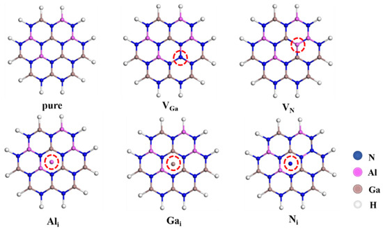
Figure 1.
The top views of different defect structures. Pure: no defect; VGa: Ga vacancy defect; VN: N vacancy defect; Ali: Al interstitial defect; Gai: Ga interstitial defect; Ni: N interstitial defect.
3. Results and Discussion
There is no doubt that both interstitial defects and vacancy defects affect the stability of the nanowire structure, and the formation energy can be used to assess the stability of Al0.5Ga0.5N nanowires with different defects. What is more, the formation energy can be calculated using the following formula [30]:
where Eperfect and Edefect represent the total energy of the structures with and without defects, respectively. ni represents the number of defect atom, and μi represents the chemical potential of the defect atom.
Figure 2a shows the calculated formation energies of different structures. It is clear that compared with the original nanowire structure, the formation process of vacancy defects is an endothermic reaction, which contributes to an unstable nanowire structure. The most difficult to survive is the N atom vacancy defect. Surprisingly, for the formation process of Al and Ga interstitial defects, it is also an endothermic process. However, it is easier to survive than the vacancy defect. Then, for the formation process of N interstitial defects, it is stable owing to negative formation energy, which is consistent with the previous conclusion [24]. According to the previous study [24], the formation energy of the outermost surface defects in the GaN nanowire was about 2.64 eV, while in this study, the formation energy of N interstitial defect at the core position is −3.47 eV. The disparity is mainly due to the differences in Al composition and doping position in the simulated nanowire structures.
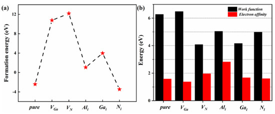
Figure 2.
(a) Formation energies of Al0.5Ga0.5N nanowires with different defects. (b) Work function and electron affinity of Al0.5Ga0.5N nanowires with different defects.
In order to quantitatively describe the effect of defects on optoelectronic properties, the work function and electron affinity are firstly calculated in this study. The work function (φ) is the energy difference between the vacuum level (Evac) and the Fermi level (Ef). The electron affinity (χ) is the energy difference between the vacuum level and the conduction band minimum (EC). The specific formula are as follows [31]:
As is shown in Figure 2b, except for Ga vacancy defects, the introduction of defects contributes to the decrease in surface work function and the slight increase in surface electron affinity. This is mainly attributed to the redistribution of electrons on the nanowire surface caused by the introduction of defects, thereby affecting the transition of photoelectrons. Importantly, it can also be confirmed by the following charge distribution.
On the other hand, the introduction of defects causes changes in the electron density and varying degrees of atom displacements near the defect. Therefore, in order to better understand the effect of introduced defects on the atomic structure and electrons of Al0.5Ga0.5N nanowires, we estimated the bond length, Barder charge distribution, and lattice constant with different defects. The calculated results are shown in Table 1. As calculated, the bond lengths of Ga-N bonds and Al-N bonds in pure Al0.5Ga0.5N nanowires are 1.986 Å and 1.905 Å, respectively, which is similar to the previous study [32]. Furthermore, it is clear in Table 1 that the Al interstitial defects lead to a significant extension of the Al-N bond, extending by 0.601 Å. Next, the interstitial defects have little effect on the Ga-N bond. Additionally, the vacancy defects lead to a decrease in Ga-N bond and Al-N bond. What is more, according to the Barder charge distribution, the initial charge values of Ga atoms, Al atoms, and N atoms in the Al0.5Ga0.5N nanowires without defects are 1.37 eV, 2.37 eV, and −1.89 eV, respectively. Regardless of interstitial defects or vacancy defects, the charge transfer of Al atoms is not obvious, and it is more obvious for Ga atoms and N atoms. Importantly, the N atom vacancy defects greatly reduce the charge of Ga atoms. The introduction of defects also contributes to the reduction in the a-axis and b-axis lattice constant and the increase in c-axis lattice constant, which indicates the closer atomic connections in the horizontal direction of Al0.5Ga0.5N nanowires.

Table 1.
Bond length, Barder charge distribution, and lattice constant of Al0.5Ga0.5N nanowires with interstitial defects and vacancy defects.
In order to further understand the effect of defects on the optoelectrical properties of Al0.5Ga0.5N nanowires, great efforts have been carried out to evaluate the band structures of different models with defects, as shown in Figure 3. It is obvious that the pure Al0.5Ga0.5N nanowire is a direct band gap semiconductor, with a band gap of 5.43 eV. In Figure 3b,c, the appearance of the acceptor energy level can be clearly observed. Compared with the pure Al0.5Ga0.5N nanowire, the band structure of Ga vacancy defect exhibits the p-type characteristic. However, for the N vacancy defect, it contributes to the band structure moving toward lower energy direction and then showing the n-type characteristic. It is mainly attributed to the fact that the vacancy atoms reduce the charge density near the defects. Figure 3d–f show that the interstitial defects introduce impurity energy levels near the Fermi level, which are represented as donor or acceptor energy levels in the energy band diagram.
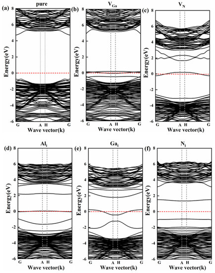
Figure 3.
Band structures of different models: (a) pure Al0.5Ga0.5N nanowires, (b) VGa, (c) VN, (d) Ali, (e) Gai, (f) Ni.
Immediately afterwards, in order to have a deeper understanding of the changes in the band structure, the partial density of states (PDOS) are also considered. Figure 4 shows the PDOS of Al0.5Ga0.5N nanowires with different defects. It can be seen from Figure 4a–c that the interstitial defects introduce a new p-type electronic state near the Fermi level and move toward the lower energy direction, thus passing through the Fermi level and showing n-type characteristics. Among them, the influence caused by Al and Ga interstitial defects is the most obvious. As shown in Figure 4d, due to the lack of N atoms, the density of states of Ga atoms moves towards lower energy as a whole and the total electronic states of Ga atoms decrease. As shown in Figure 4e, due to the lack of Ga atoms in the core position, the peak value of the total electronic states of N atoms has been reduced. Meanwhile, the electronic state of the N atom at the Fermi level is no longer zero and has certain p-type structural characteristics.
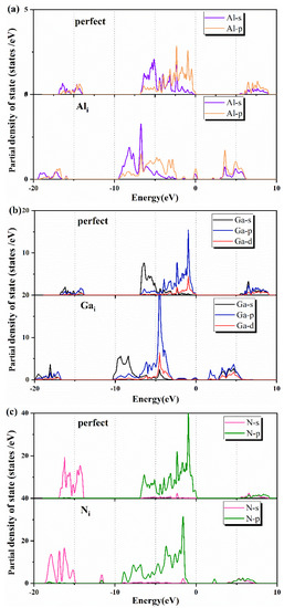
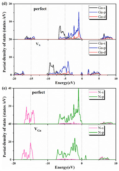
Figure 4.
Partial density of states (PDOS) of different defect structures: (a) Ali, (b) Gai, (c) Ni, (d) VN, (e) VGa.
4. Conclusions
In summary, based on the first-principles calculation method, we have investigated the effects of interstitial defects and vacancy defects on the electronic structure of Al0.5Ga0.5N nanowires. From the perspective of formation energy, only the N interstitial defect is an exothermic reaction, which contributes to a thermally stable nanowire structure. In Al0.5Ga0.5N nanowire, interstitial defects are more likely to stably exist than vacancy defects. In addition, except for the Ga vacancy defect, other impurity types cause the work function of the nanowire surface to decrease and the electron affinity to increase. This is mainly due to the decrease in the conduction band minimum in band structures caused by the introduction of defects. Furthermore, the introduction of defects cause changes in the electron density and varying degrees of atom displacements near the defects. In others, the introduction of different defects leads to new donor or acceptor energy levels near the Fermi level in the band structures, making the different nanowires exhibit n-type or p-type characteristics. Overall, this research aims to reveal the effect of different defects on the electronic properties of Al0.5Ga0.5N nanowires, and to provide systematical guidance for subsequent experimental preparation.
Author Contributions
Methodology, Q.F.; software, X.Y. and L.Y.; validation, S.Z; formal analysis, Y.L.; investigation, X.Y.; resources, Q.F. and S.Z.; writing—original draft preparation, Y.L.; writing—review and editing, Y.S.; visualization, L.Y.; supervision, Y.S.; project administration, L.C.; funding acquisition, Y.S. All authors have read and agreed to the published version of the manuscript.
Funding
This work was supported by the National Natural Science Foundation of China (Grant Nos. 62,004,183 and 62075205), Natural Science Foundation of Zhejiang Province (Grant Nos. LQ21F050011 and LZ20F050001) and the Fundamental Research Funds for the Provincial Universities of Zhejiang (Grant Nos. 2020YW48, 2021YW11 and 2021YW87).
Institutional Review Board Statement
Not applicable.
Informed Consent Statement
Not applicable.
Data Availability Statement
Not applicable.
Acknowledgments
We thanks Jianguo Wan from Nanjing University for providing us with first-principles computational resources.
Conflicts of Interest
The authors declare no conflict of interest.
References
- Mizuno, S. Acoustic Phonon Modes and Phononic Bandgaps in GaN/AlN Nanowire Superlattices. Nanoscale Res. Lett. 2012, 7, 479. [Google Scholar] [CrossRef] [PubMed]
- Jayaprakash, R.; Ajagunna, D.; Germanis, S.; Androulidaki, M.; Tsagaraki, K.; Georgakilas, A.; Pelekanos, N.T. Extraction of Absorption Coefficients from as-Grown GaN Nanowires on Opaque Substrates Using All-Optical Method. Opt. Express 2014, 22, 19555–19566. [Google Scholar] [CrossRef]
- Nam, C.-Y.; Jaroenapibal, P.; Tham, D.; Luzzi, D.E.; Evoy, S.; Fischer, J.E. Diameter-Dependent Electromechanical Properties of GaN Nanowires. Nano Lett. 2006, 6, 153–158. [Google Scholar] [CrossRef] [PubMed]
- Kim, S.S.; Park, J.Y.; Choi, S.W.; Kim, H.S.; Na, H.G.; Yang, J.C.; Lee, C.; Kim, H.W. Room Temperature Sensing Properties of Networked GaN Nanowire Sensors to Hydrogen Enhanced by the Ga2Pd5 Nanodot Functionalization. Int. J. Hydrog. Energy 2011, 36, 2313–2319. [Google Scholar] [CrossRef]
- Sergent, S.; Damilano, B.; Vézian, S.; Chenot, S.; Tsuchizawa, T.; Notomi, M. Lasing Up to 380 K in a Sublimated GaN Nanowire. Appl. Phys. Lett. 2020, 116, 223101. [Google Scholar] [CrossRef]
- Routray, S.; Lenka, T. Performance Analysis of Nanodisk and Core/Shell/Shell-Nanowire Type III-Nitride Heterojunction Solar Cell for Efficient Energy Harvesting. Superlattices Microstruct. 2017, 111, 776–782. [Google Scholar] [CrossRef]
- Mao, S.; Liu, Y.; Li, P.; Meng, X. Fabrication and Comparative Study of Vertically Grown and Horizontally-Dispersed Fully Nanowire-Based Photodetectors. Appl. Surf. Sci. 2015, 359, 496–499. [Google Scholar] [CrossRef]
- Memisevic, E.; Hellenbrand, M.; Lind, E.; Persson, A.R.; Sant, S.; Schenk, A.; Svensson, J.; Wallenberg, R.; Wernersson, L.-E. Individual Defects in InAs/InGaAsSb/GaSb Nanowire Tunnel Field-Effect Transistors Operating below 60 mV/Decade. Nano Lett. 2017, 17, 4373–4380. [Google Scholar] [CrossRef]
- Roy, A.; Mead, J.; Wang, S.; Huang, H. Effects of Surface Defects on the Mechanical Properties of ZnO Nanowires. Sci. Rep. 2017, 7, 9547. [Google Scholar] [CrossRef]
- Wang, J.; Wang, J.G.; Qin, X.; Wang, Y.; You, Z.; Liu, H.; Shao, M. Superfine MnO2 Nanowires with Rich Defects toward Boosted Zinc Ion Storage Performance. ACS Appl. Mater. Interfaces 2020, 12, 34487–35766. [Google Scholar] [CrossRef]
- Heo, J.; Cho, K.-H.; Jain, P.K. Motion of Defects in Ion-Conducting Nanowires. Nano Lett. 2020, 21, 556–561. [Google Scholar] [CrossRef] [PubMed]
- Dai, S.; Zhao, J.; He, M.-R.; Wang, X.; Wan, J.; Shan, Z.; Zhu, J. Elastic Properties of GaN Nanowires: Revealing the Influence of Planar Defects on Young’s Modulus at Nanoscale. Nano Lett. 2014, 15, 8–15. [Google Scholar] [CrossRef] [PubMed]
- Hemesath, E.R.; Schreiber, D.K.; Gulsoy, E.B.; Kisielowski, C.F.; Petford-Long, A.K.; Voorhees, P.W.; Lauhon, L.J. Catalyst Incorporation at Defects during Nanowire Growth. Nano Lett. 2011, 12, 167–171. [Google Scholar] [CrossRef] [PubMed]
- Biswas, S.; Barth, S.; Holmes, J.D. Inducing Imperfections in Germanium Nanowires. Nano Res. 2017, 10, 1510–1523. [Google Scholar] [CrossRef]
- Chen, W.; Yu, L.; Misra, S.; Fan, Z.; Pareige, P.; Patriarche, G.; Bouchoule, S. Incorporation and Redistribution of Impurities into Silicon Nanowires during Metal-Particle-Assisted Growth. Nat. Commun. 2014, 5, 4134. [Google Scholar] [CrossRef]
- Alvarez, A.D.; Peric, N.; Vergel, N.A.F.; Nys, J.-P.; Berthe, M.; Patriarche, G.; Harmand, J.-C.; Caroff, P.; Plissard, S.; Ebert, P.; et al. Importance of Point Defect Reactions for the Atomic-Scale Roughness of III–V Nanowire Sidewalls. Nanotechnology 2019, 30, 324002. [Google Scholar] [CrossRef]
- Xia, S.; Liu, L.; Kong, Y.; Wang, H.; Wang, M. Study of Cs Adsorption on (100) Surface of [1]-Oriented GaN Nanowires: A First Principle Research. Appl. Surf.Sci. 2016, 387, 1110–1115. [Google Scholar] [CrossRef]
- Srivastava, M.; Srivastava, A. Electron Transport in CO2 Adsorbed ZnO Nanowire: DFT Study. Chem. Phys. Lett. 2019, 729, 17–23. [Google Scholar] [CrossRef]
- Tan, T.L.; Ng, M.-F. Computational Screening for Effective Ge1−xSix Nanowire Photocatalyst. Phys. Chem. Chem. Phys. 2015, 17, 20391–20397. [Google Scholar] [CrossRef]
- Shu, H.; Yang, X.; Liang, P.; Cao, D.; Chen, X. Impact of Surface Point Defects on Electronic Properties and P-Type Doping of GaAs Nanowires. J. Phys. Chem. C 2016, 120, 22088–22095. [Google Scholar] [CrossRef]
- Liao, H.; Li, J.; Wei, T.; Wen, P.; Li, M.; Hu, X. First-Principles Study of CN point defects on sidewall surface of [0 0 0 1]-oriented GaN nanowires. Appl. Surf. Sci. 2018, 467, 293–297. [Google Scholar] [CrossRef]
- Kong, Y.; Liu, L.; Xia, S.; Wang, H.; Wang, M. Research on Optoelectronic Properties of GaN Nanowires with N Vacancy. Comput. Theor. Chem. 2016, 1092, 19–24. [Google Scholar] [CrossRef]
- Liu, L.; Diao, Y.; Xia, S. Intrinsic Point Defects in Pristine and Zn-Doped GaAs Nanowire Surfaces: A First-Principles Investi-gation. Appl. Surf. Sci. 2020, 514, 145906. [Google Scholar] [CrossRef]
- Lu, F.; Liu, L.; Tian, J. Optoelectronic Properties Exploration of Native Point Defects on GaN Nanowires. Appl. Surf. Sci. 2021, 565, 150600. [Google Scholar] [CrossRef]
- Hafner, J. Materials Simulations Using VASP—A Quantum Perspective to Materials Science. Comput. Phys. Commun. 2007, 177, 6–13. [Google Scholar] [CrossRef]
- Hafner, J. ChemInform Abstract: Ab-Initio Simulations of Materials Using VASP: Density-functional Theory and Beyond. ChemInform 2008, 39, 2044–2078. [Google Scholar] [CrossRef]
- Perdew, J.P.; Burke, K.; Ernzerhof, M. Generalized Gradient Approximation Made Simple. Phys. Rev. Lett. 1996, 77, 3865. [Google Scholar] [CrossRef]
- Dinh, P.M.; Messud, J.; Reinhard, P.G.; Suraud, E. Self-Interaction Correction in a Simple Structure. Phys. Lett. A 2008, 372, 5598–5602. [Google Scholar] [CrossRef]
- Wang, D.; Tang, L.-M. Electronic Structure and Magnetism of Doped Wurtzite InSb Nanowire. J. Phys. D Appl. Phys. 2016, 49, 175303. [Google Scholar] [CrossRef]
- Wang, Z.; Li, J.; Gao, F.; Weber, W.J. Defects in Gallium Nitride Nanowires: First Principles Calculations. J. Appl. Phys. 2010, 108, 044305. [Google Scholar] [CrossRef]
- Zou, J.; Chang, B.; Yang, Z.; Zhang, Y.; Qiao, J. Evolution of Surface Potential Barrier for Negative-Electron-Affinity GaAs Photo-Cathodes. J. Appl. Phys. 2019, 105, 013714. [Google Scholar] [CrossRef]
- Yang, M.; Fu, X.; Guo, J.; Rao, W. Electronic Structure and Optical Properties of Al0.25Ga0.75N with Point Defects and Mg-Defect Complexes. Opt. Quantum Electron. 2018, 50, 60. [Google Scholar] [CrossRef]


Publisher’s Note: MDPI stays neutral with regard to jurisdictional claims in published maps and institutional affiliations. |
© 2022 by the authors. Licensee MDPI, Basel, Switzerland. This article is an open access article distributed under the terms and conditions of the Creative Commons Attribution (CC BY) license (https://creativecommons.org/licenses/by/4.0/).