Abstract
The micro-hole machining of quartz wafers depends on photolithography techniques akin to those used in semiconductor fabrication. These methods present challenges due to high equipment setup costs, large space requirements, and environmental pollution risks. This research applies ultrasonic vibration assistance in electrochemical discharge machining to create an array of micro-holes on quartz wafers. In the experiments, a self-prepared tungsten carbide micro-electrode array served as the tool electrode. This electrode was a 2 × 2 square array, with needles measuring 30 × 30 μm. A series of experiments was conducted to investigate the effects of various machining parameters, including working voltage, feed rate, duration time, duty factor, and ultrasonic power level, on the characteristics of the micro-hole array. The characteristics included average hole diameter and through-hole surface morphology. The experimental objective was to achieve a through-hole diameter of 80 μm with an accuracy of ±8 μm. During the electrochemical discharge machining, suitable ultrasonic vibrations can thin the insulating gas film coating on the electrode surface, resulting in a more uniform gas film. As the insulating gas film’s thickness decreased, so did the critical voltage needed for the electrochemical discharge machining, reducing the hole’s diameter expansion. The ultrasonic vibration assistance can enable the satisfaction of the dimensional accuracy requirement. The experimental results indicate that ultrasonic vibration assistance can effectively improve the processing capacity and reduce sample fragmentation. A working voltage of 44 V, feed rate of 1 μm/6 s, duration time of 30 μs, duty factor of 30%, and ultrasonic power level of 1 resulted in better inlet and outlet surface morphology without outlet fragmentation. Moreover, the average diameters of the inlet and outlet were roughly 80 μm while meeting the through-hole diameter of 80 μm with accuracy of ±8 μm.
1. Introduction
With the rapid development of science and technology in recent years, the demand for sensing components and micro-electromechanical systems (MEMS) increased significantly in terms of application areas, such as 5G communication, Artificial Intelligence (AI), Internet of Vehicles/Things, AR/VR, smart homes, and the optoelectronics industry. With such advantages as high chemical stability, excellent optical properties, low coefficient of thermal expansion, high mechanical strength and high surface evenness, the quartz wafer becomes an ideal material for micro-electromechanical component manufacturing. However, the processing of quartz wafers is rather challenging due to their high hardness and brittleness. Cracks and defects often occur in the traditional mechanical manufacturing process, especially in micro- and complex structures. The quartz wafer can be processed using a semiconductor process, which uses a large amount of highly corrosive electrolytes and has a great impact on the environment and human health, as well as expensive infrastructure. Therefore, how to develop a more effective manufacturing and processing method to reduce the cost and improve production efficiency is a very important topic.
Electrochemical discharge machining (ECDM) is a high-efficiency and high-precision processing technology. It is often used to process non-conductive materials that are difficult to process, such as quartz wafers and ceramic materials [1]. ECDM is a composite processing method. Its basic principle is electrochemical reaction and electrical spark discharge, with high-temperature melting and etching-assisted processing, using the energy of electrical spark discharge to rapidly increase the temperature of the local electrolyte so as to accelerate the material etching. It can be used to make micro-structures on quartz wafers.
In the course of ECDM, the electrolyte near the tool electrode undergoes strong electrolysis, continuously producing bubbles on the electrode surface, and the micro-bubbles gradually gather to form large bubbles, which are combined into an insulating gas film covering the surface of the tool electrode. When the applied working voltage is high enough to break through the insulating gas film, a discharge spark is generated between the tool electrode and the workpiece. The discharge energy can melt the workpiece, and the high heat energy thereof can partially heat up the electrolyte, accelerating the chemical etching of the workpiece by the electrolyte. However, at the middle and later stages of micro-hole processing, the electrolyte renewal is unsatisfactory due to a small processing gap. Hence, the gas film at the front end of the electrode cannot remain in a stable state, resulting in a sharp decline in the processing capability [2]. The insulating gas film can be thinned by rotating the tool electrode, and the material removal rate and the aspect ratio of ECDM micro-holes are improved [3]. Since there are micro-hole arrays designed on the surface of current quartz wafers, if only a single micro-hole is processed each time, the processing time is prolonged, and the cost is too high. This problem can be solved by using an array electrode for electrochemical discharge grinding and broaching [4]. However, when the array electrode needle is very small, it is difficult to perform electrochemical discharge grinding and broaching on the micro-array electrode because of its low strength. Moreover, the array electrode is inapplicable to rotary processing, so the generated bubbles are likely to accumulate between the electrode needles. The discharge sparks concentrate on the side of the electrode where the bubbles accumulate, resulting in non-uniform discharge on various surfaces of the micro-array electrode needles, as well as bad processing capability. Therefore, this study used ultrasonic vibration-assisted ECDM and micro-array electrodes to study the quartz wafer micro-hole array processing. The micro-array electrode can increase the micro-hole processing efficiency by multiples, and the ultrasonic vibration can promote the renewal of electrolytes in micro-holes. Thus, the insulating gas film can be thinned, the material removal rate is increased greatly [5,6], the processing capability is improved, and the processing accuracy is improved. As a result, the average inlet and outlet diameters can reach the target dimensional accuracy of 80 ± 8μm.
2. Experimental Settings and Methods
2.1. Experimental Structure
2.1.1. Experimental Instruments
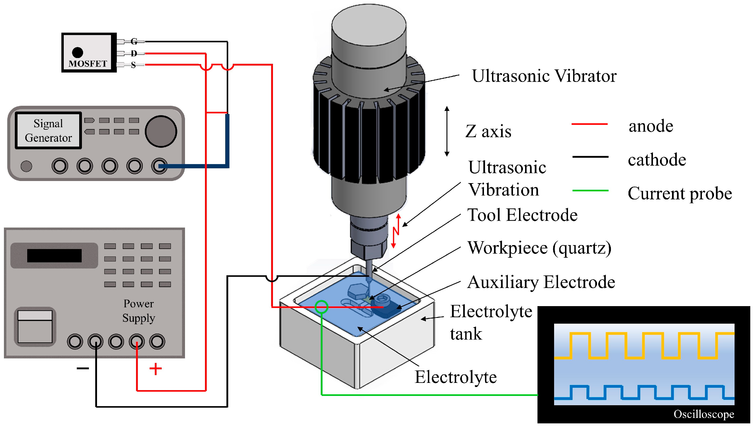
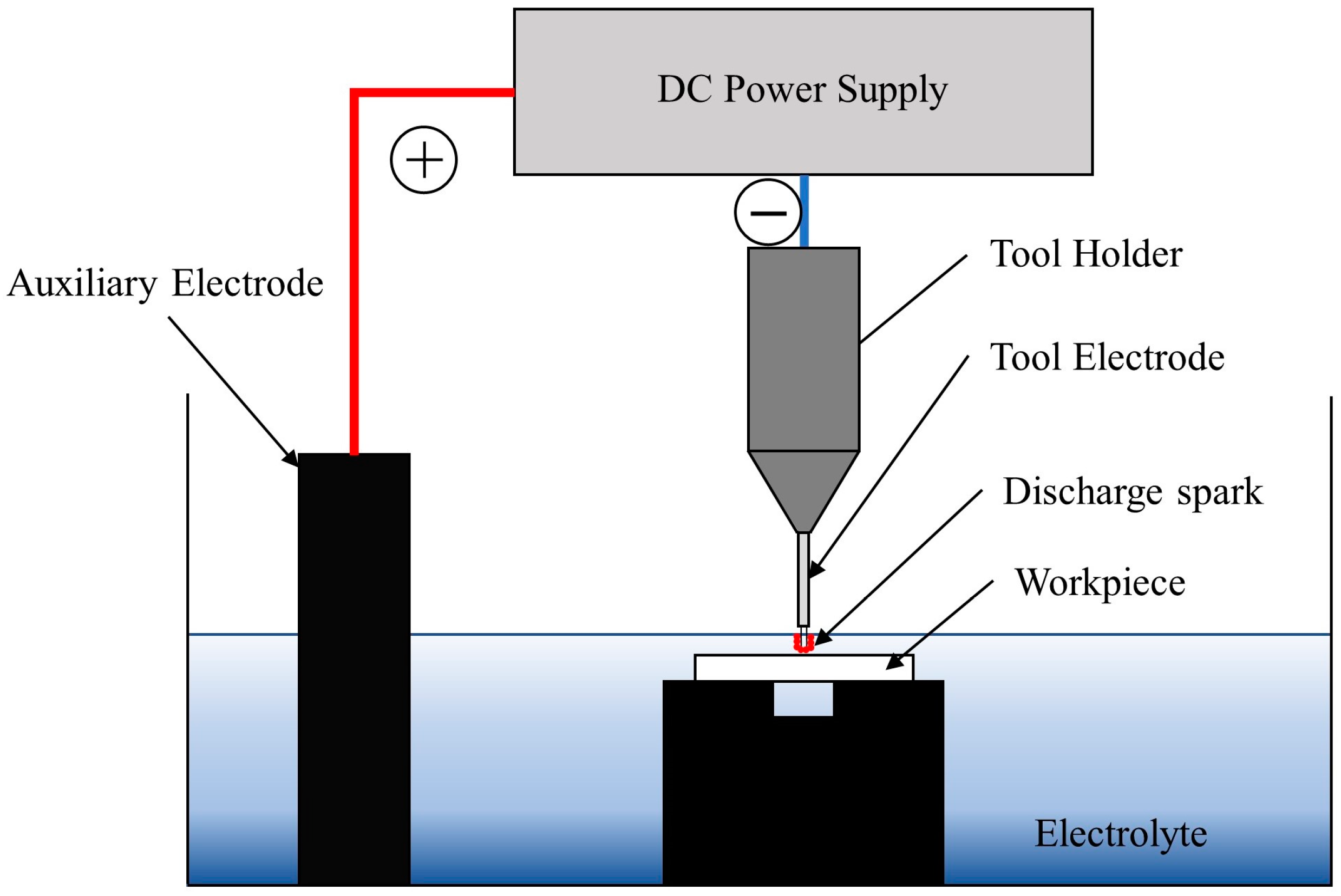
The schematic diagram of the equipment setup for this experiment is shown in Figure 1. The electrochemical discharge machine has an automatic feed function and can move up and down independently on the Z-axis. In addition, an ultrasonic vibrator produced by Acrow Machinery Mfg. is disposed of on the Z-axis. The ultrasonic tool holder clamps a tool electrode to apply axial ultrasonic vibration during the experiment. The graphite is used as an auxiliary electrode, which is settled in the processing tank, and the quartz wafer workpiece is clamped in the processing tank. The processing tank contains electrolytes, and the processing energy is supplied in the form of a DC power supply and a signal generator. The tool electrode and auxiliary electrode are connected to the cathode and anode of the power supply, respectively. The processing current waveform is measured by an oscilloscope. The pulse bias is generated due to the additional N-type metal-oxide-semiconductor field-effect transistor (MOSFET) of the DC power supply and signal generator. Due to this device, the working voltage only drops by 10 V and does not completely return to zero during the pulse-off time of the duration time. Hence, the stability of the insulating gas film is maintained [7].
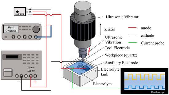
Figure 1.
The schematic diagram of the equipment setup.
2.1.2. Experimental materials
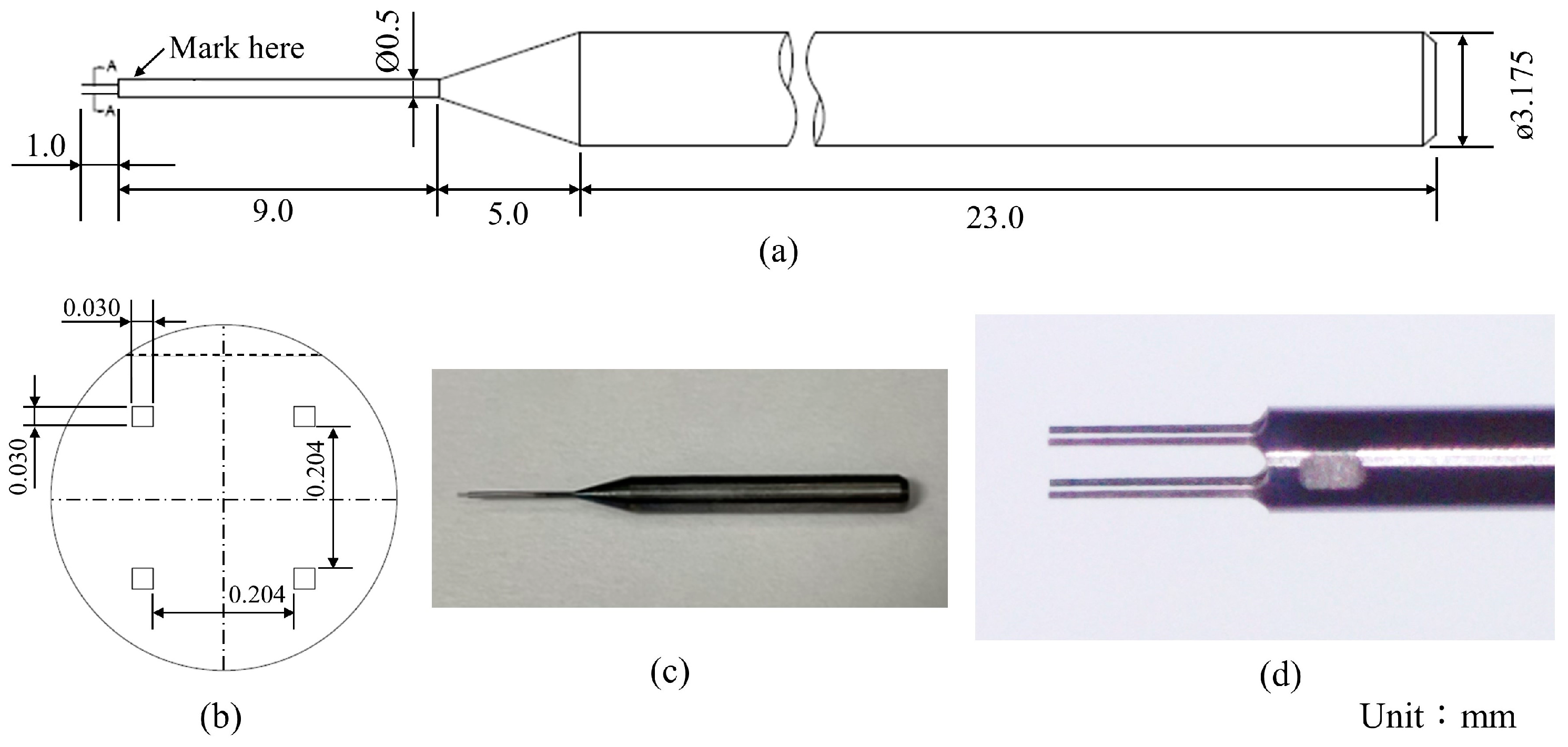
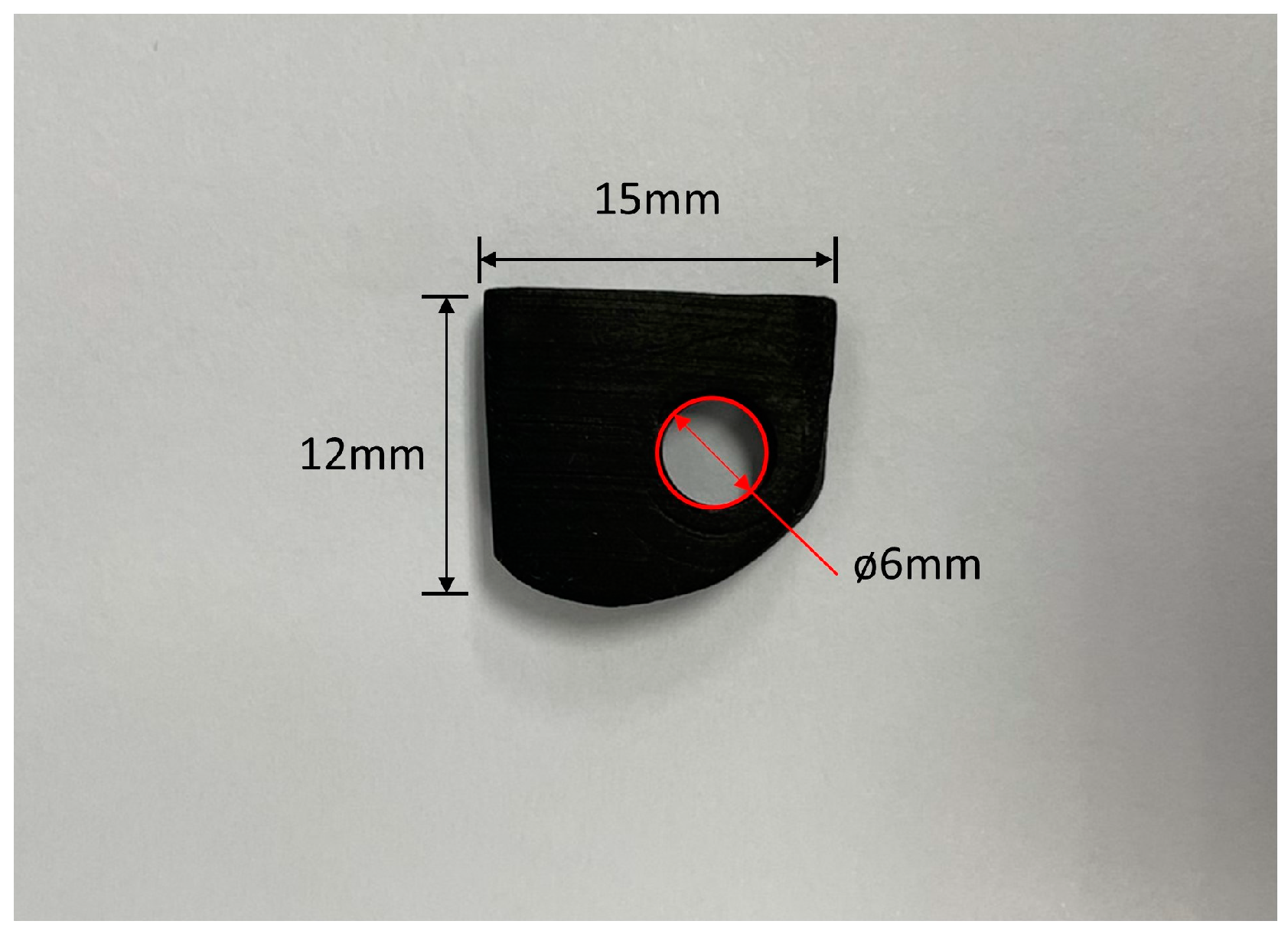
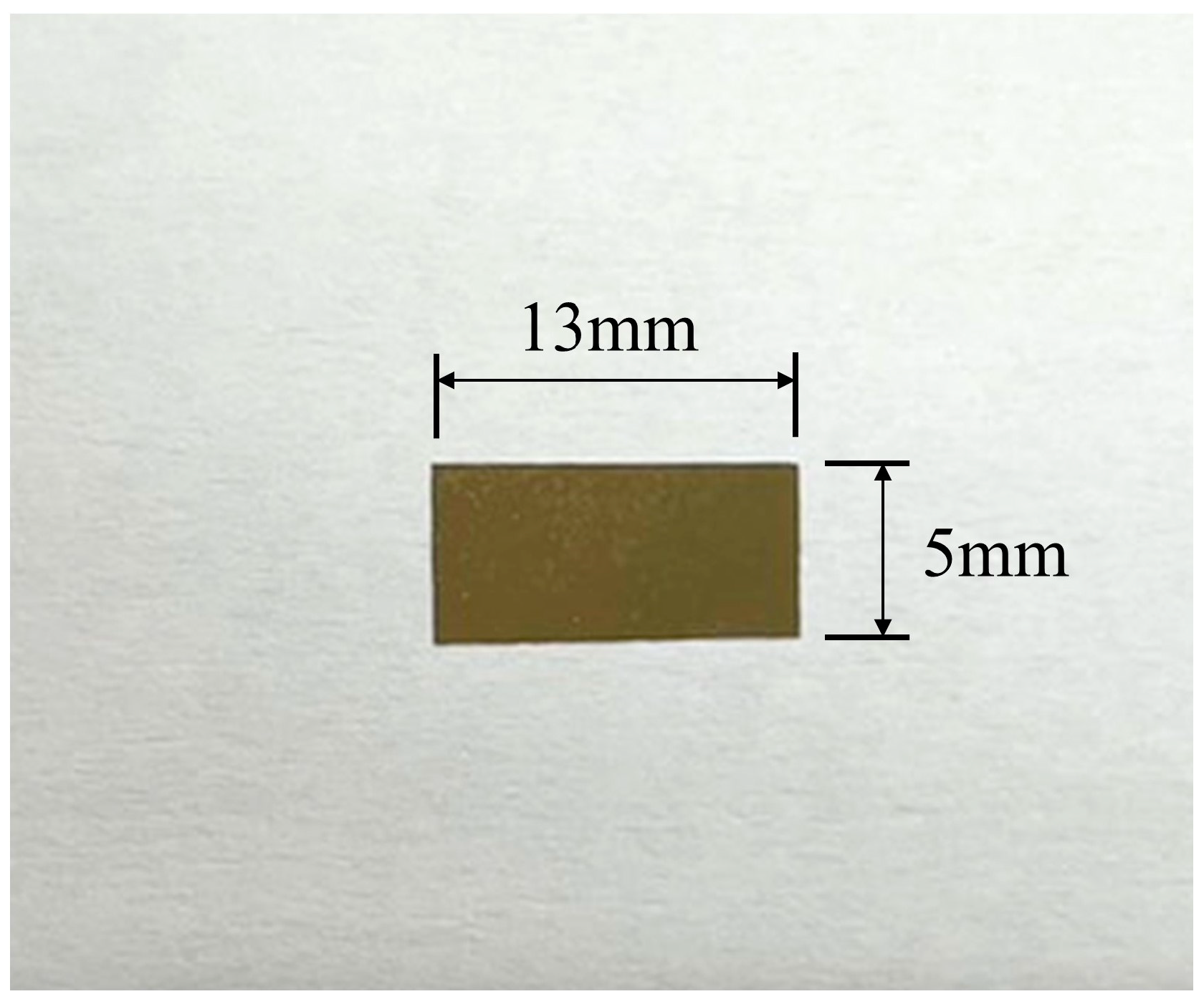
The micro-tool electrode was a 2 × 2 tungsten carbide array electrode. There were four needles at the front end of the tool electrode. The size of each needle was 30 × 30 μm. The needles were processed by WEDG, as shown in Figure 2. The specifications are shown in Table 1. The auxiliary electrode was graphite. Because of its excellent chemical stability, it was not electrolyzed during the processing and did not affect the experimental results, as shown in Figure 3. The thickness of the quartz wafer sample to be processed was 70 μm; the quartz wafer of 2-inch diameter was cut into small pieces of 13 × 5 mm in advance, which can be locked in the processing tank. The surface was coated with gold film for contact alignment between the tool electrode and the workpiece, as shown in Figure 4.
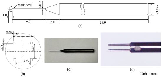
Figure 2.
The micro-tool electrode. (a) Schematic diagram of the micro-array electrode. (b) A-A profile of the micro-array electrode. (c) Photo of micro-array electrode. (d) Enlarged photo of the micro-array electrode.

Table 1.
The compositions of the iron-based metallic glass.
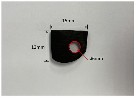
Figure 3.
The graphite auxiliary electrode.
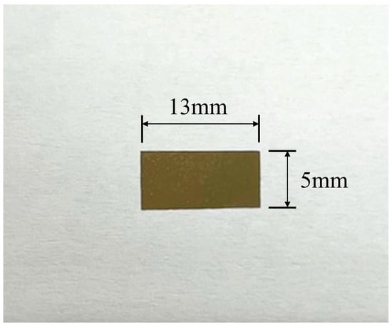
Figure 4.
The photo of quartz wafer sample.
2.2. Fundamental Theory
2.2.1. Electrochemical Discharge Mechanism
The tool electrode and auxiliary electrode were immersed in the electrolyte at the same time, and a DC voltage was applied to form a current loop between the positive and negative electrodes. The hydrogen bubbles adhering to the surface of the tool electrode (negative electrode) merged and grew into a dense insulating gas film. If the applied voltage exceeds the critical voltage, the insulating gas film layer is broken through, and discharge sparks are generated. The high temperature derived from the discharge sparks can melt and evaporate the surface of the workpiece, and the high temperature and heat generated can heat the electrolyte, increasing the chemical etching rate and improving the material removal rate. The basic configuration of ECDM is shown in Figure 5.

Figure 5.
The basic configuration of ECDM [8].
2.2.2. Chemical Etching
The main component of quartz material is SiO2. The alkaline electrolyte KOH is used to etch the quartz wafer material in this experiment. The chemical equation is expressed as follows:
SiO2 + 2KOH + H2O → Si(OH)4 + K2O,
Si(OH)4 + KOH → [Si(OH)3O]-K+ + H2O
The quartz material reacts with alkaline solution at room temperature very slowly. Looking at the relationship between the chemical reaction rate constant (KA) and temperature, the relation is expressed as follows:
KA(T) = Ae(-E/RT)
A = frequency factor
E = activation energy J/mol or cal/mol
K = 1.987 cal/mol*K
R = gas constant = 8.314 J/mol*K
T = absolute temperature (K)
According to the above equation, the high temperature around the electrical discharge machining area accelerates the chemical etching of the quartz material by the strong alkali solution, and the etching rate increases exponentially.
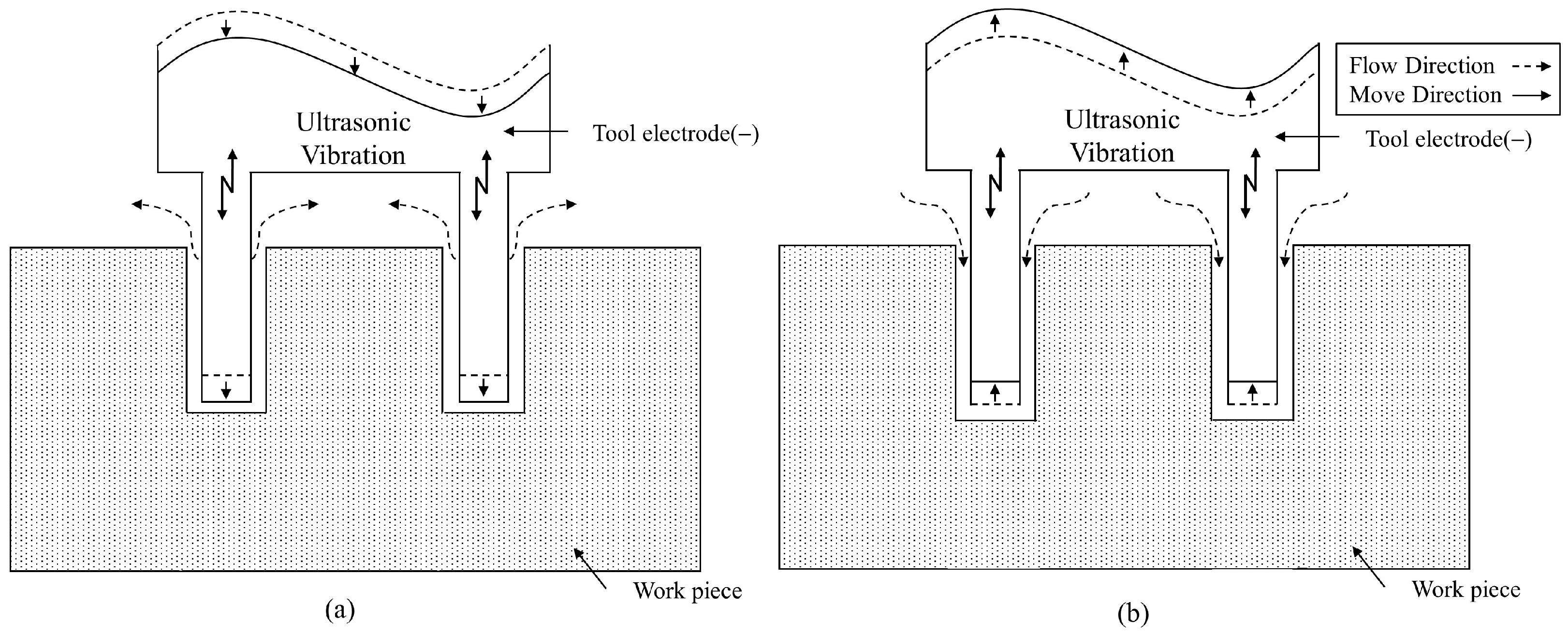
2.2.3. Ultrasonic Pumping Effect
Ultrasonic-assisted machining refers to applying ultrasonic vibration to the tool electrode to suck and squeeze the electrolyte in the machining gap so that the electrolyte is squeezed out and sucked into the machining gap, resulting in a pumping effect. The circular renewal of electrolytes in the micro-holes is promoted, and the insulating gas film can be thinned. As a result, the material removal rate is increased greatly, and the processing efficiency is increased, as shown in Figure 6 [9].
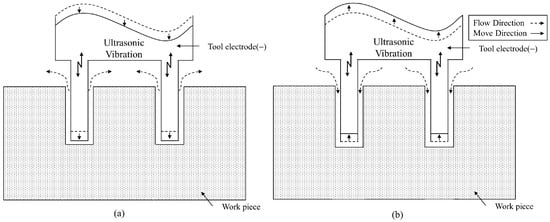
Figure 6.
Schematic diagram of ultrasonic pumping effect. (a) Electrode moves downward. (b) Electrode moves upward.
2.3. Experimental Method
In this experiment, a pulse power supply and the assistance of ultrasonic vibration were used for ECDM of quartz wafer array micro-holes. After the tool electrode was installed on the ultrasonic tool holder, pulse bias power was applied for processing. The initial gap between the tool electrode and the workpiece was set as 10 μm, and then the Z-axis was moved to perform feeding at a fixed speed. The single-factor experimental method was used for this experiment. The single-factor parameter settings are shown in Table 2. The fixed-factor parameter settings are shown in Table 3. The duration time and the duty factor are defined as follows:
Table 2.
Single-factor parameter.
Table 3.
Fixed-factor parameter.
The inlet and outlet diameters and sample surface morphology were measured using a microscopic image-measuring instrument. The surface microstructure was observed through the SEM so as to understand the influence of various processing parameters on the inlet and outlet diameters of the micro-hole array and micro-hole morphology after processing.
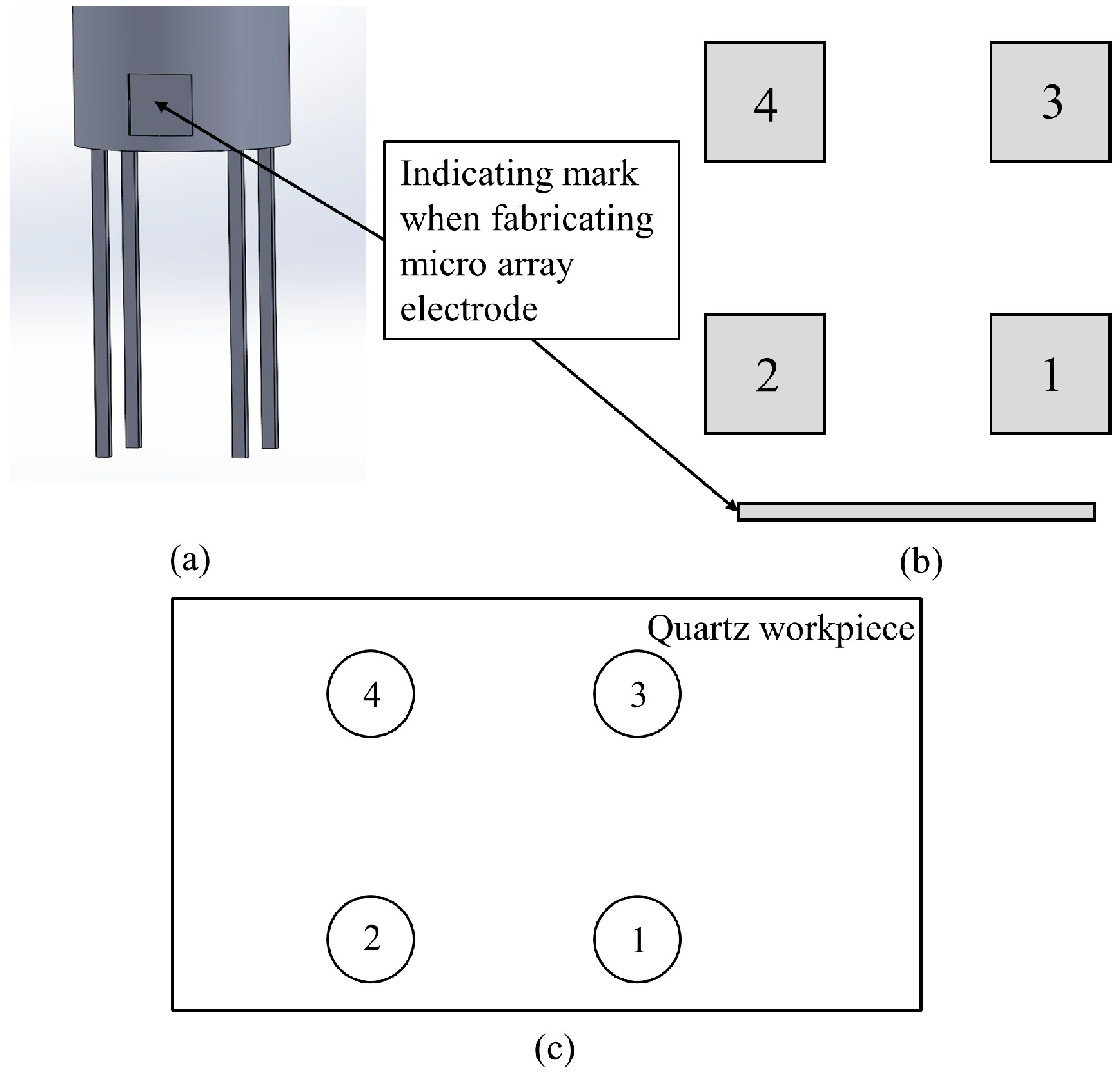
Since the array electrode has 4 needles, in order to confirm the micro-hole number, during the preparation of the array electrode using the WEDG equipment, the mark is machined at the upper ends of the needles, as shown in Figure 7a. The positions of the needles of the array electrode can thus be defined and numbered. The numbering method is shown in Figure 7b. The numbers of the array micro-holes correspond to the numbers of the array electrode needles, and the numbering method is shown in Figure 7c. The amplitude of the ultrasonic vibration was measured by the laser ultrasonic amplitude measuring device (UTC65). It is employed to measure the amplitude displacement values corresponding to different power levels of the ultrasonic oscillator settings during the experimental tool electrode. The ultrasonic oscillator can generate ultrasonic vibration frequency at 26 kHz with its power-adjustable knob in 10 levels.

Figure 7.
Schematic diagram of the serial number on the micro-array electrode. (a) The indicating mark on the side of micro-array electrode. (b) Serial numbering method. (c) Serial number on the workpiece.
3. Experimental Results and Discussion
3.1. Comparison of Processing with and without the Assistance of Ultrasonic Vibration
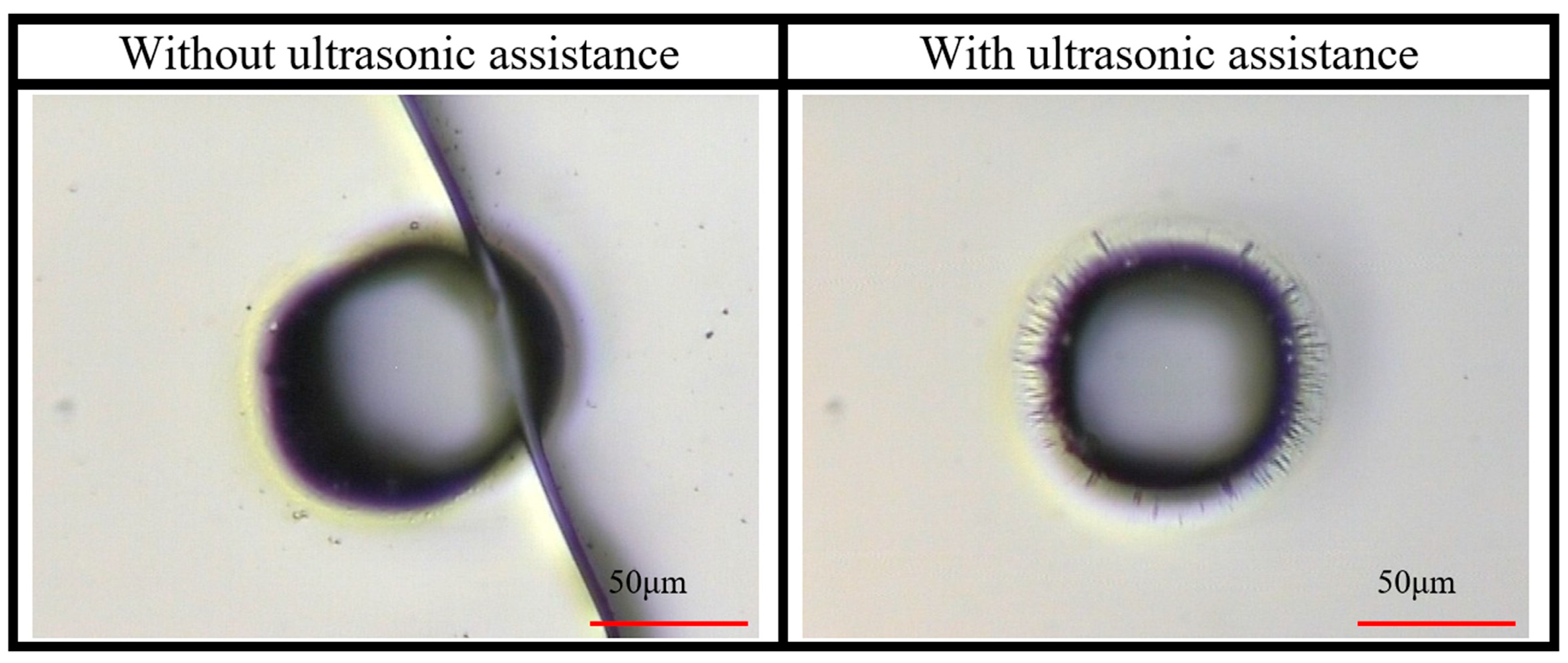
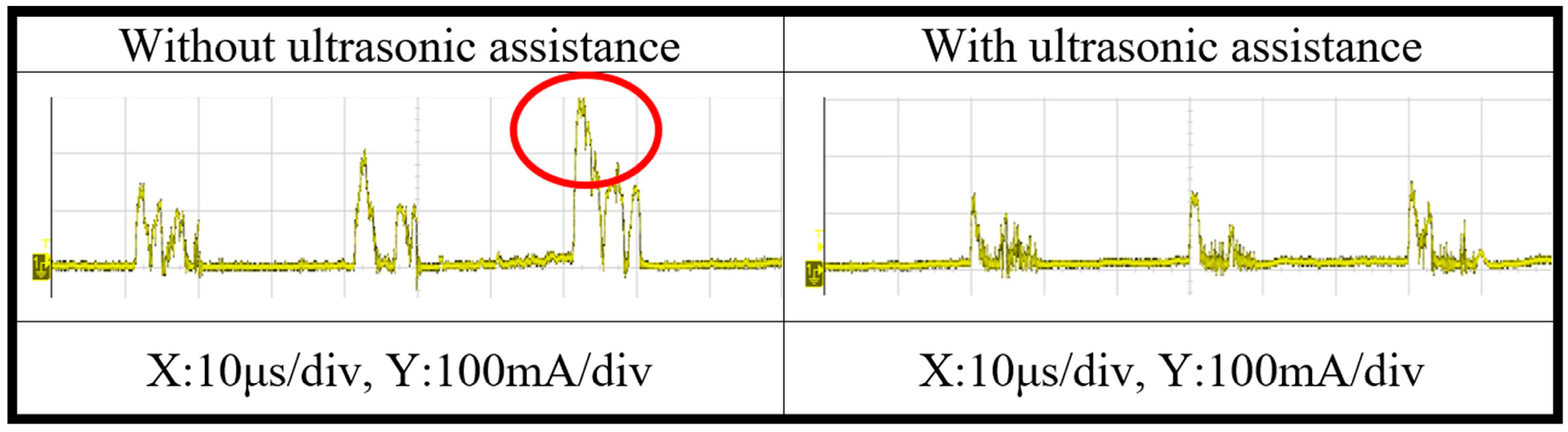
In order to confirm the influence of the assistance of ultrasonic vibration on electrochemical discharge array micro-hole machining, this study first conducted an experiment on a comparison of the cases with and without the assistance of ultrasonic vibration. It also conducted an experiment on ultrasonic vibration-assisted electrochemical discharge array micro-hole machining when the ultrasonic power level was 1. The parameter combination of the working voltage of 44 V, feed rate of 1 μm/6 sec, duration time of 30 μs, and duty factor of 30% was used so as to compare the results of processing with and without the assistance of ultrasonic vibration. Figure 8 shows the results of processing with and without the assistance of ultrasonic vibration. The results of processing without the assistance of ultrasonic vibration show that there are ruptures in the quartz wafer. In ECDM, without the assistance of ultrasonic vibration, the gas film formation is relatively unstable [10], thus resulting in a decrease in the material removal rate. Hence, during axial downward feed processing, the front end of the working electrode directly contacts the quartz wafer workpiece, leaving an insufficient processing gap at the front end of the electrode for the electrolyte to flow through and be renewed, resulting in poor material removal. The working electrode continuously squeezes the quartz wafer workpiece while advancing, and finally, the workpiece is ruptured by the extrusion. The results of processing with the assistance of ultrasonic vibration show that there is no rupture of the quartz wafer, and the morphology of the hole is good. In addition, the state of the discharge current waveform is an important reference index that can directly reflect whether the gas film structure is stable and dense. Figure 9 shows the current waveforms with and without the assistance of ultrasonic vibration. As observed, in the processing without the assistance of ultrasonic vibration, the current waveform changes drastically and is in a relatively unstable state. There are also many current waveforms of electrolyzed water, as shown in the red circle in the figure. The higher current represents the phenomenon of electrolysis of water. The current waveform, with the assistance of ultrasonic vibration, is relatively stable, and there is no current waveform of electrolyzed water; the processing performance is better. To further understand the influence of other processing parameters on ECDM characteristics with the assistance of ultrasonic vibration, single-factor experiments on various process parameters with the assistance of ultrasonic vibration are conducted.
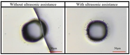
Figure 8.
The results of processing without and with the assistance of ultrasonic vibration.
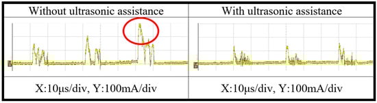
Figure 9.
The current waveforms without and with the assistance of ultrasonic vibration.
3.2. Effects of Different Parameters on Electrochemical Discharge Array Micro-Hole Machining
3.2.1. Effect of Working Voltage on Electrochemical Discharge Array Micro-Hole Machining
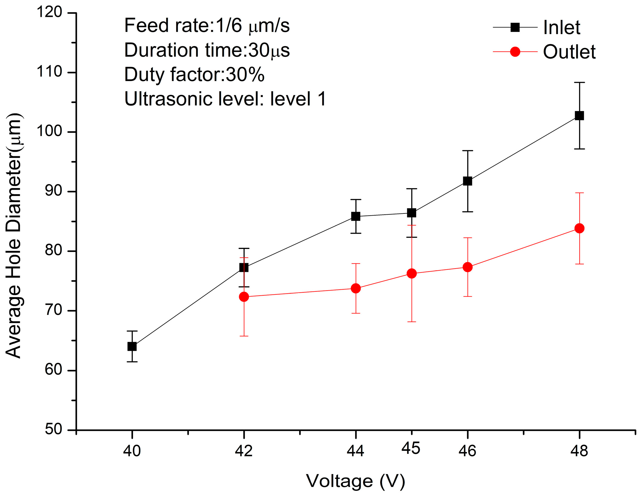
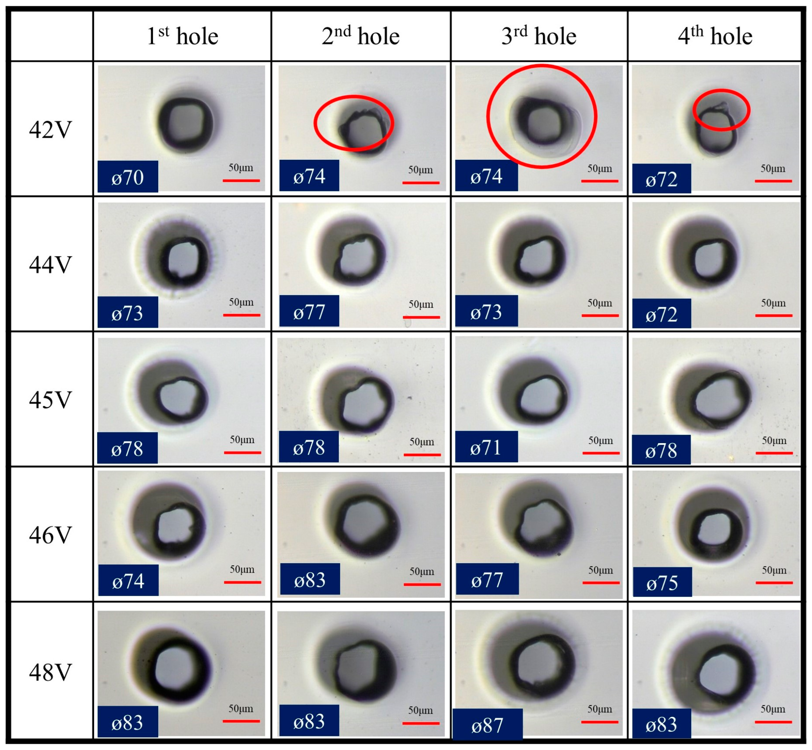
Figure 10 shows the relationships of the working voltage to the average inlet and outlet diameters. The average inlet and outlet diameters of the array micro-holes increase with the increase in working voltage. When the working voltage is increased from 42 V to 48 V, the average inlet diameter is increased from 77.3 μm to 102.8 μm, and the average outlet diameter is increased from 72.3 μm to 83.8 μm because when the working voltage is increased, the bubble formation rate is increased, the insulating gas film is thicker, and the discharge energy is higher, and the average inlet and outlet diameters of the array micro-holes is increased as the working voltage increasing. In addition, as shown in Figure 10, when the working voltage is 40 V, the array through-holes cannot be formed smoothly, as the applied voltage is too low, and the energy is insufficient to form a dense gas film, resulting in an overly low material removal rate. Afterward, the analysis of the influence of the working voltage of 40 V on various quality characteristics is eliminated, and an additional experiment on the working voltage of 45 V is conducted so as to know the changes in the quality characteristics between the working voltages 44 V and 46 V. When the working voltage is 44 V, the average inlet diameter is 85.8 μm, and the average outlet diameter is 73.8 μm. When the working voltage is 45 V, the average inlet diameter is 86.4 μm, and the average outlet diameter is 76.5 μm. Both of the working voltage parameters can meet the target dimensional accuracy of 80 ± 8 μm, and there is no fragment at the outlet of the array micro-holes. As shown in Figure 11, when the working voltage is 45 V, the electrolysis of water occurs, resulting in unstable discharge, as well as material removal deviating from the center of the circle at the inlet of No. 1 hole and No. 3 hole, as shown in Figure 11. When the working voltage is 42 V, there are fragments at the array micro-hole outlet, as shown in the red circle in Figure 12 where the working voltage is 42 V. This condition shows that due to insufficient processing capability, when the tool electrode penetrates the workpiece to form a through-hole, the working electrode directly squeezes the workpiece and ruptures it. The morphology of the array micro-holes is relatively poor when the working voltage is 45 V.

Figure 10.
The relationships of the average inlet and outlet diameters to the working voltage.
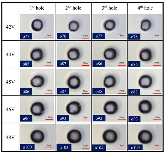
Figure 11.
The inlet hole morphology under different working voltages.

Figure 12.
The outlet hole morphology under different working voltages.
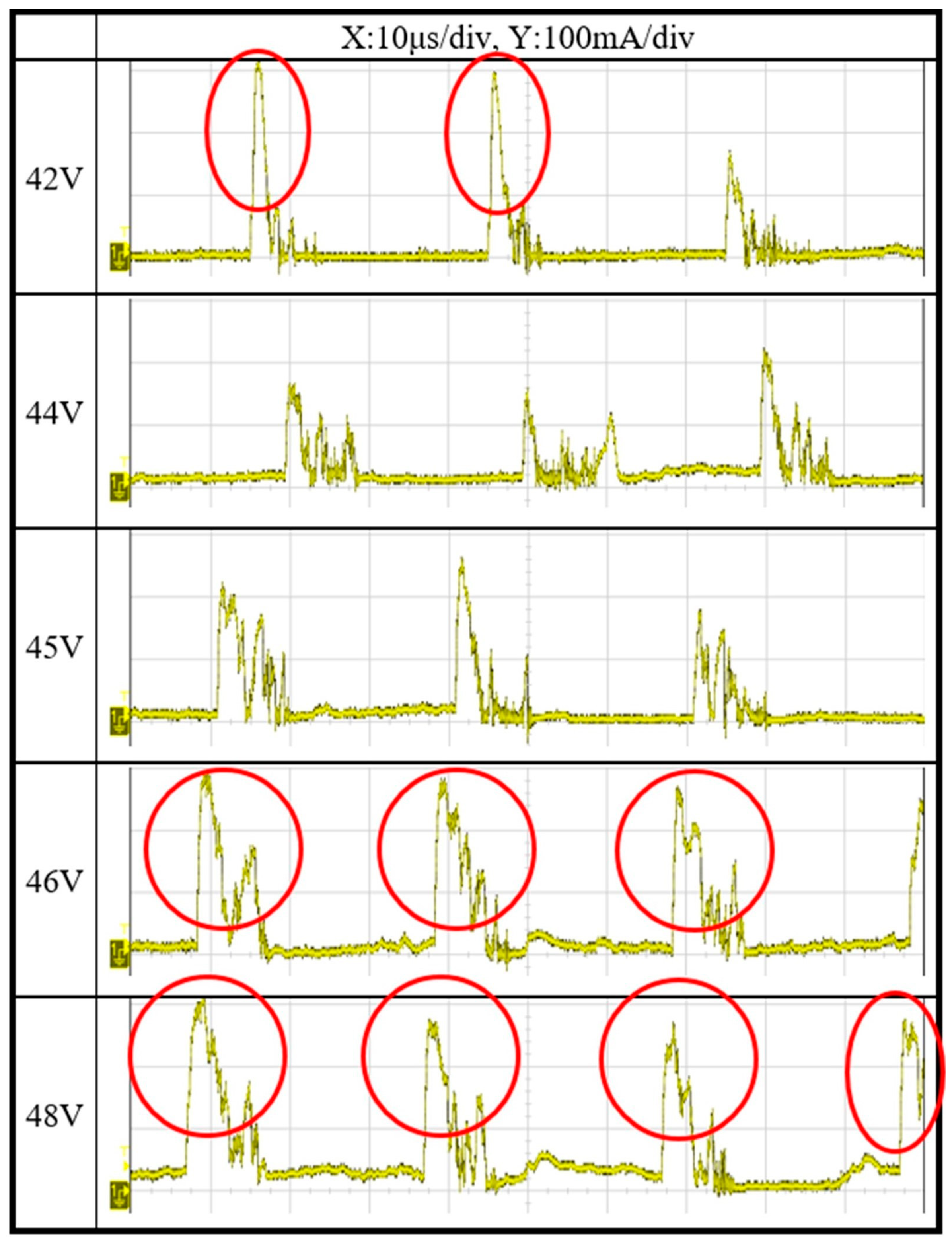
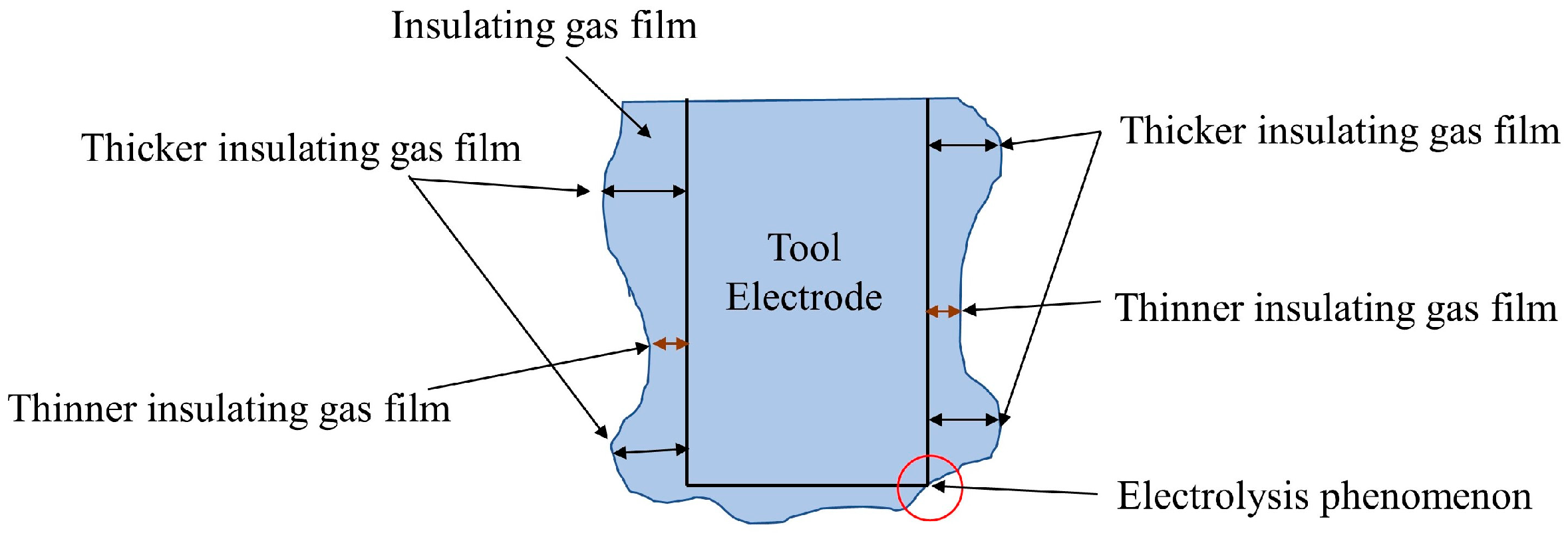
When the working voltage is 42 V, the processing current and the discharge number are lower than that of the other working voltage parameters. As the working voltage is too low, the gas film structure is unstable, and the electrolysis current waveform is likely to occur, as shown in the red circle of working voltage 42 V in Figure 13. The higher current represents the phenomenon of electrolysis of water. When the working voltage is higher than 46 V, the applied working voltage is too high, the bubble formation rate is high, and a part of the bubbles separate from the tool electrode surface under the effect of buoyancy before they are combined into an insulating gas film, the insulating gas film is disturbed excessively. Figure 14 shows the uneven thickness of the insulating gas film; the insulating gas film is partially thick, generating a high discharge current, and the thin part generates a low discharge current. The partial electrode surface even directly contacts the electrolyte due to the unstable insulating gas film, resulting in more electrolysis current waveforms, as shown in the red circles of working voltages 46 V and 48 V in Figure 13.
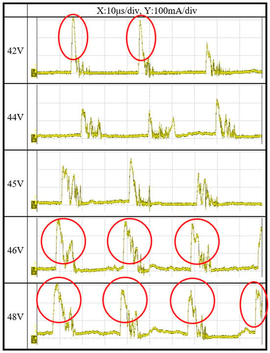
Figure 13.
The current distribution under different working voltages.

Figure 14.
Schematic diagram of uneven thickness of insulating gas film.
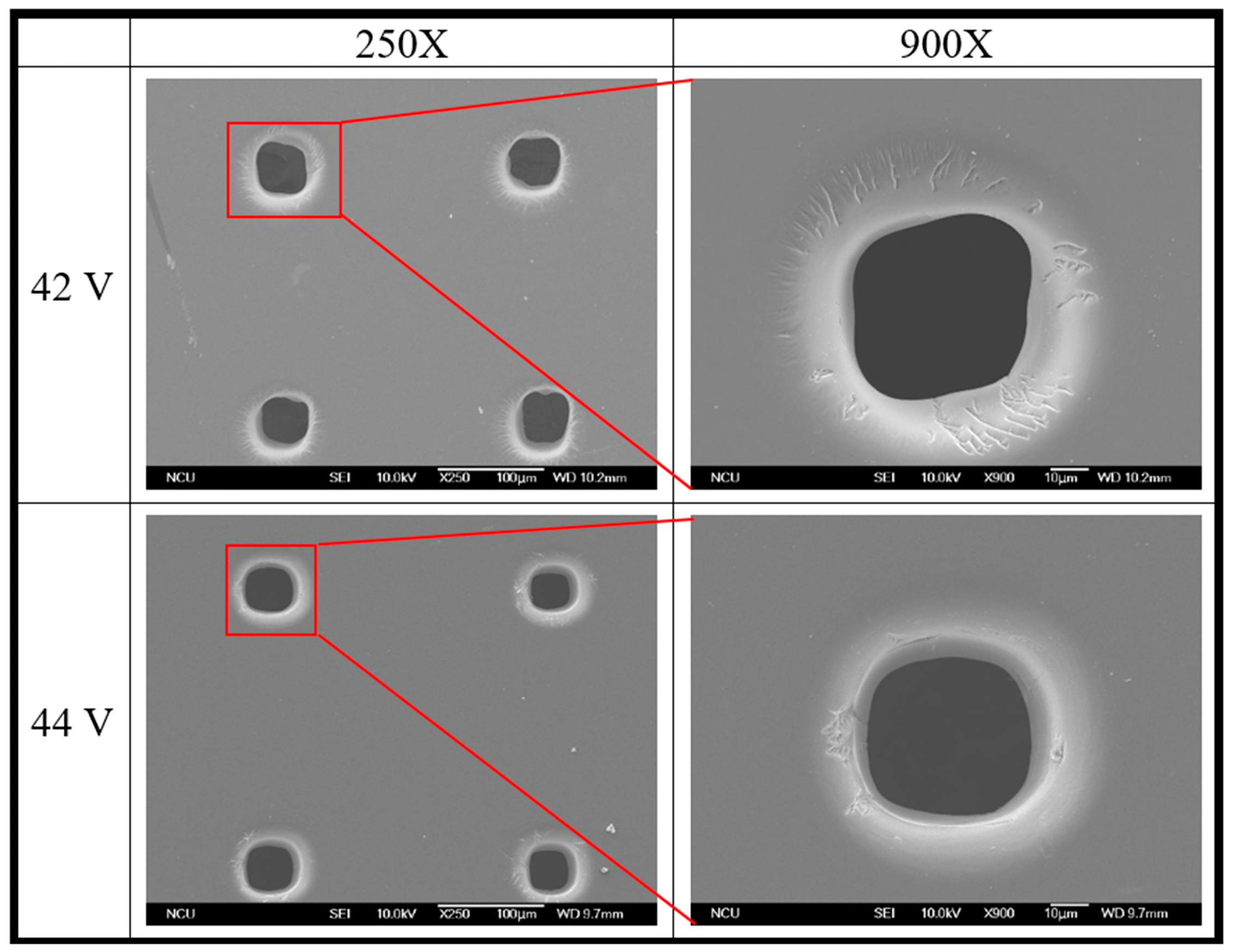
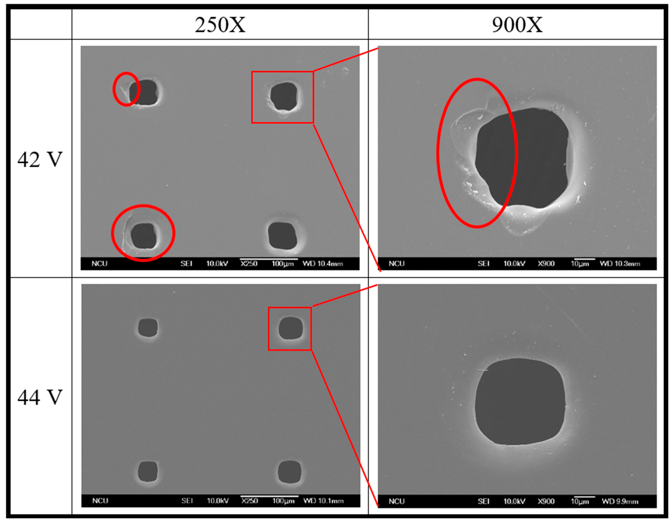
Figure 15 shows the SEM photos of the best and the worst inlet hole morphology under different working voltages. It is observed that when the working voltage is 42 V, the outline of the array micro-holes is rugged and not smooth. Figure 16 shows the SEM photos of the best and the worst outlet hole morphology under different working voltages. As observed, under the magnification of 250, there are multiple micro-hole outlet fragmentations, and the outline of the array of micro-holes is also rugged and not smooth, as shown in the red circle. Under the magnification of 900, the outlet fragmentation and raised unremoved material are observed, as shown in the red circle in Figure 16. The contour of the array micro-holes is relatively smooth, and there is no material unremoved or outlet fragmentation when the working voltage is 44 V. When the working voltage is 44 V, the array micro-hole morphology is better, so the working voltage of 44 V is selected for next experiments.
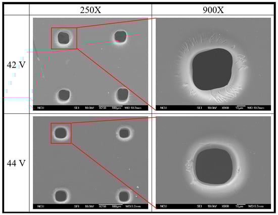
Figure 15.
The SEM photos of the worst (42 V) and the best (44 V) inlet hole morphology under different working voltages.
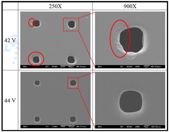
Figure 16.
The SEM photos of the worst (42 V) and the best (44 V) outlet hole morphology under different working voltages.
3.2.2. Effect of Feed Rate on Electrochemical Discharge Array Micro-Hole Machining
Figure 17 shows the relationships of the feed rate to the average inlet and outlet diameter. The average inlet and outlet diameters increase with the decrease in feed rate. When the feed rate is decreased from 1/3 μm/s to 1/7 μm/s, the average inlet diameter is increased from 78.3 μm to 86.7 μm, and the average outlet diameter is increased from 64.3 μm to 72.1 μm. At a low feed rate, as the total processing time is relatively long and the lateral discharging time is increased, the array micro-holes are enlarged. When the feed rate is 1/6 μm/s, the average inlet diameter is 85.8μm, and the average outlet diameter is 73.8 μm. When the feed rate is 1/7 μm/s, the average inlet diameter is 86.7 μm, and the average outlet diameter is 72.1 μm. Both feed rate parameters can meet the target dimensional accuracy of 80 ± 8 μm, and there is no outlet fragmentation. However, when the feed rate is 1/7 μm/s, the average outlet diameter is too close to the lower limit of the target dimensional accuracy, so this parameter is not used.
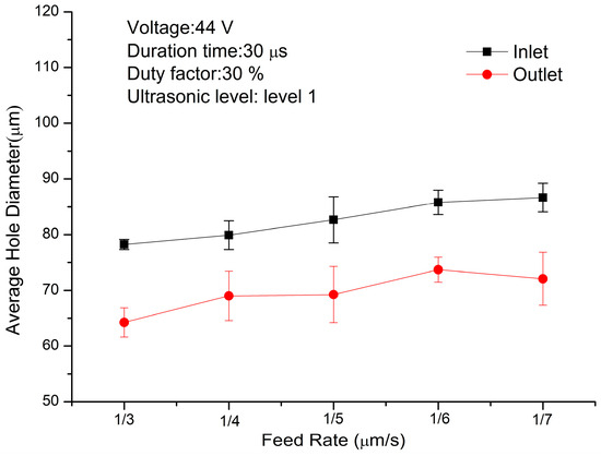
Figure 17.
The relationships of the average inlet and outlet diameters to the feed rate.
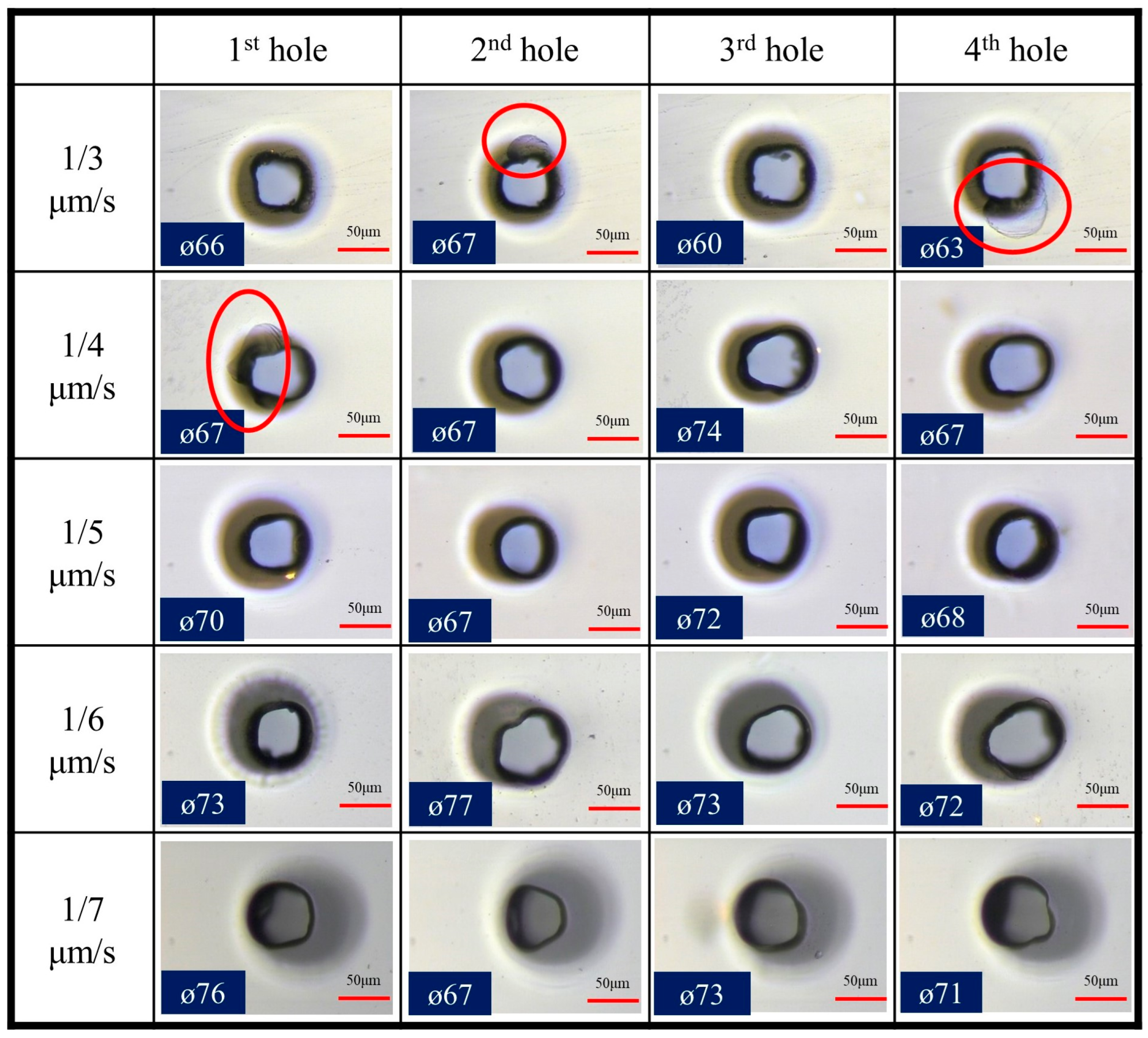
Figure 18 shows the inlet diameters and morphologies at different feed rates. Figure 19 shows the outlet diameters and morphologies at different feed rates. When the feed rate is 1/3 μm/s and 1/4 μm/s, respectively, there is obvious outlet fragmentation. As can be seen in the red circle in Figure 19, the material removal rate fails to keep up with the feed rate because the feed rate is too high. The workpiece directly contacts the tool electrode, and it is squeezed and ruptured by the tool electrode.
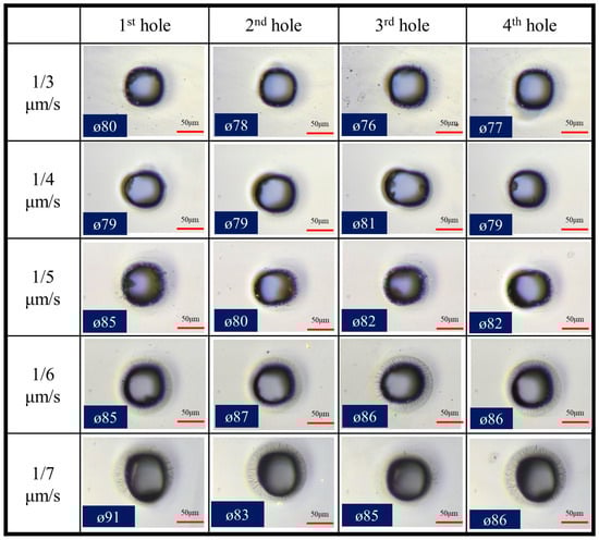
Figure 18.
The inlet hole morphology under different feed rates.

Figure 19.
The outlet hole morphology under different feed rates.
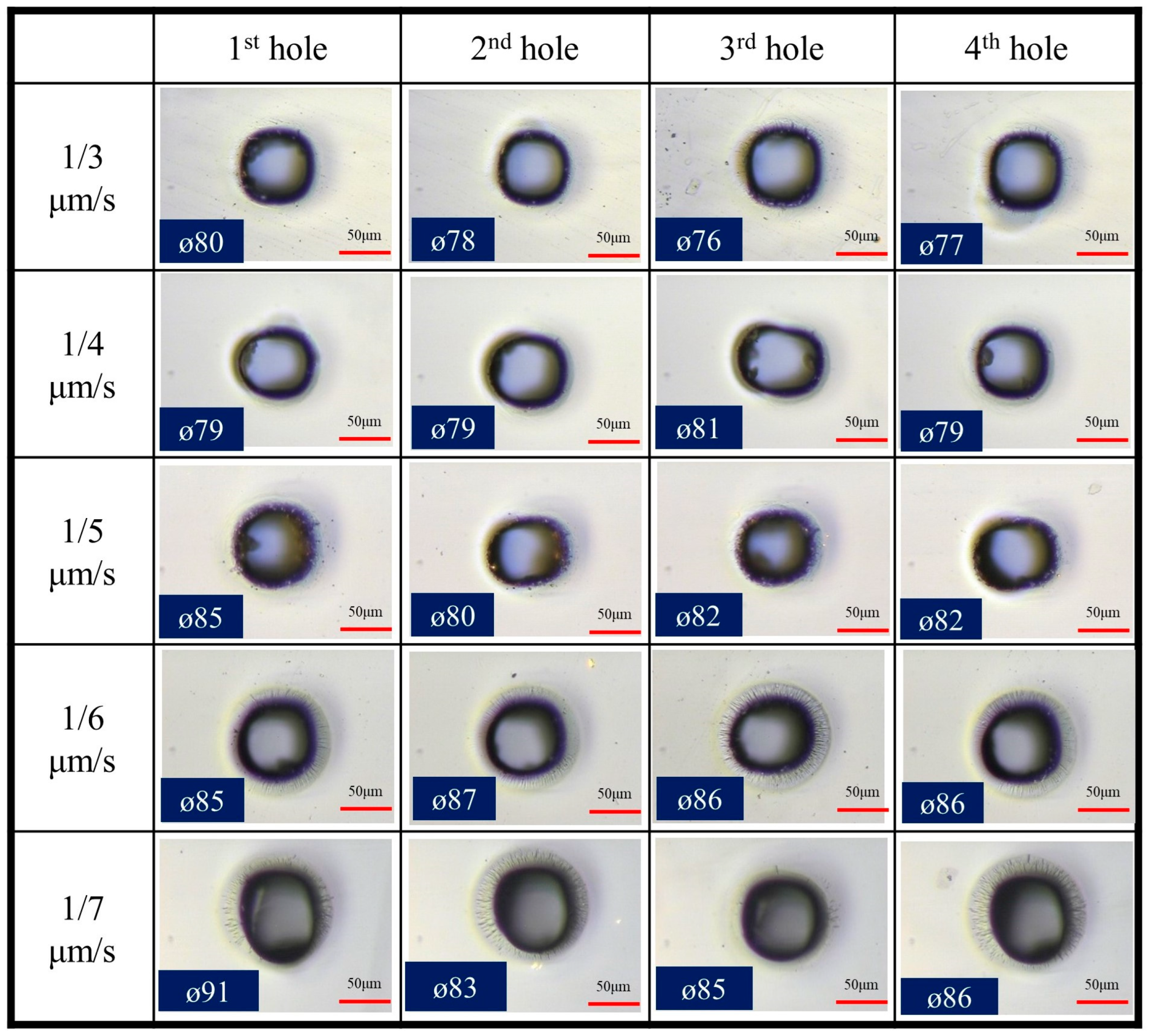
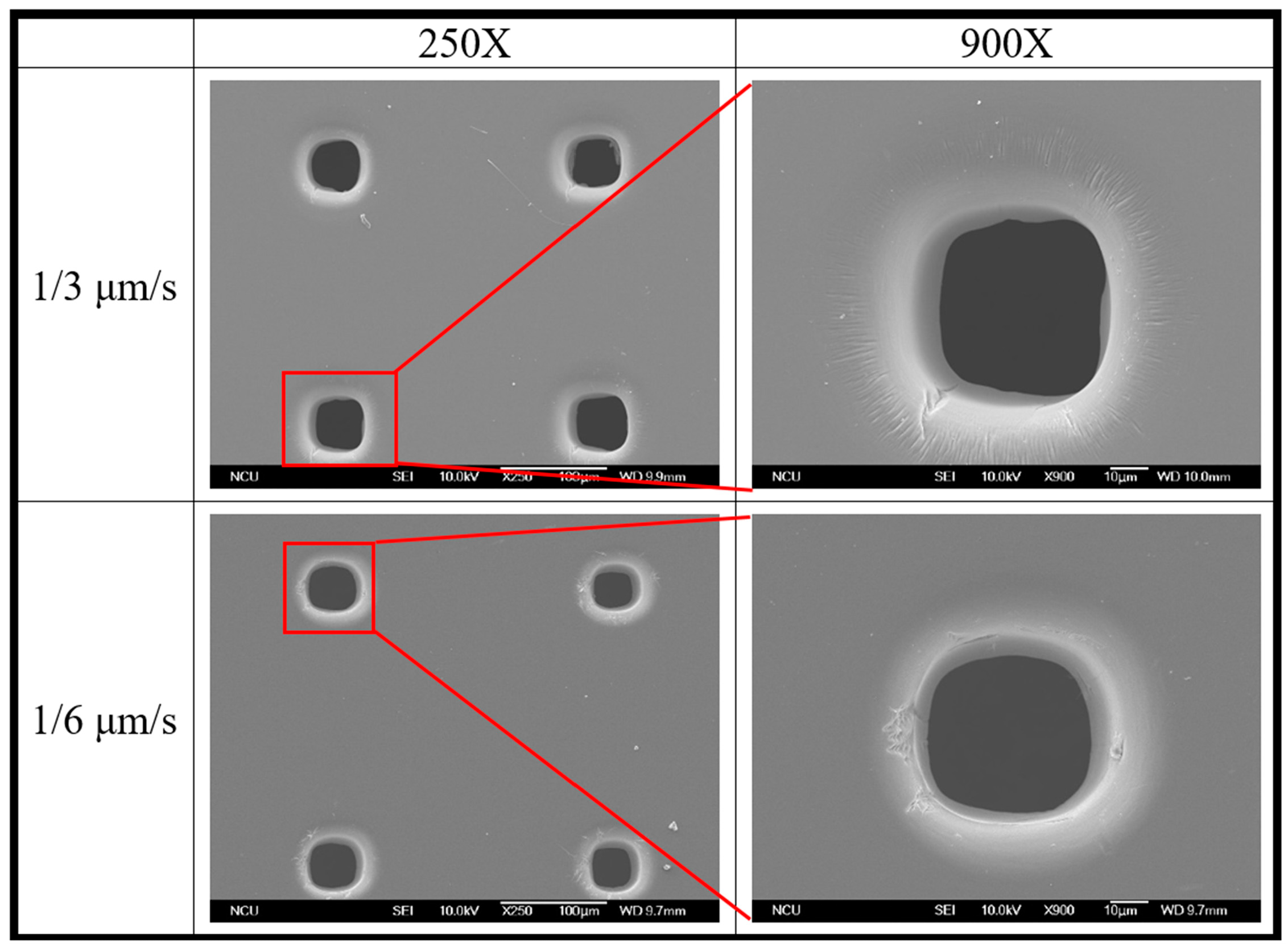
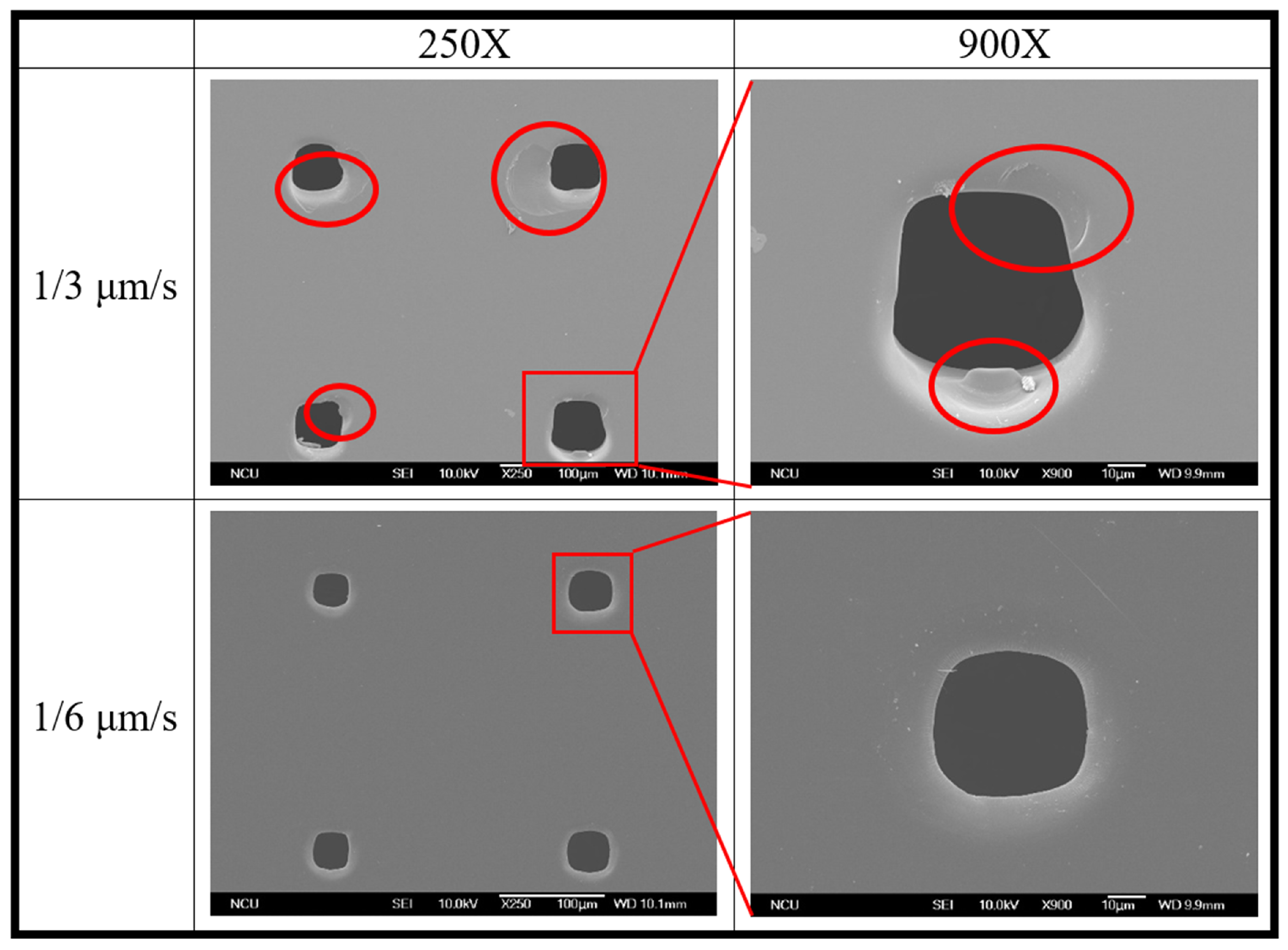
Figure 20 and Figure 21 show the SEM photos of the best and the worst inlet hole morphology under different feed rates. According to the morphologies of the array micro-holes under the magnifications of 250 and 900, when the feed rate is 1/3 μm/s, the outline of the micro-holes is rough. According to the micro-hole outlet morphology in Figure 21, under the magnification of 250, there are multiple micro-hole outlet fragmentations, and the outline is rough, as shown in the red circle. Under the magnification of 900, in addition to the outlet fragments, there is also a raised portion of material that has not been removed, as shown in the red circle in Figure 21. In contrast, the micro-hole morphology of the feed rate of 1/6 μm/s is relatively smooth, and there is no unremoved material or outlet fragmentation.

Figure 20.
The SEM photos of the worst (1/3 μm/s) and the best (1/6 μm/s) inlet hole morphology under different feed rates.
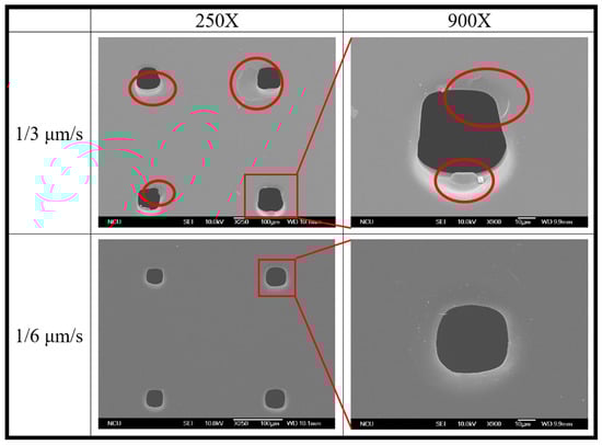
Figure 21.
The worst (1/3 μm/s) and the best (1/6 μm/s) SEM outlet hole morphology under different feed rates.
3.2.3. Effect of Duration Time on Electrochemical Discharge Array Micro-Hole Machining
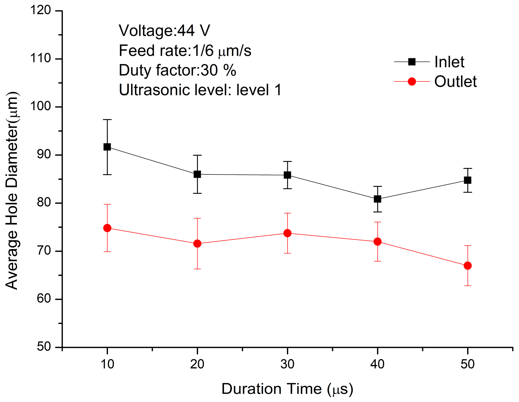
Figure 22 shows the relationships of the duration time to the average inlet and outlet diameter. The average inlet diameter is decreased from 91.7 μm to 80.8 μm as the duration time is increased from 10 μs to 40 μs, and the average inlet diameter is increased from 80.8 μm to 85.1 μm as the duration time is increased from 40 μs to 50 μs. When the duration time is 10 μs, as the pulse-off time is too short, the next duration time is entered before the insulating gas film is completely dissipated, and the energy supply continues at the next pulse-on time. Bubbles are formed continuously to accumulate the insulating gas film, and a thick insulating gas film is formed. In order to break through the thick insulating gas film, higher discharge energy is required, resulting in a large hole enlargement. When the duration time is 40 μs, the discharge off time is enough for the insulating gas film to dissipate. To produce the next discharge phenomenon, the insulating gas film is formed again, so the discharge time is short, and the array micro-hole enlargement is small. When the duration time is 50 μs, as the pulse-on time is increased, the discharge time is relatively long, resulting in a large average inlet diameter. When the duration time increases from 10 μs to 50 μs, the average outlet diameter decreases from 74.8 μm to 68.3 μm. Because the duration time of 50 μs is relatively long, and the pulse-on time is long, the bubbles at the front end of the electrode move upward under the effect of buoyancy and accumulate at the upper edge of the electrode. As a result, there are fewer bubbles at the front end of the electrode, resulting in an unstable insulating gas film and relatively weak processing capability near the outlet. Therefore, the average diameter of the outlet is decreased, as shown in Figure 22. When the duration time is 30 μs, the average inlet diameter is 85.8 μm, and the average outlet diameter is 73.8 μm. When the duration time is 40 μs, the average inlet diameter is 80.8 μm, and the average outlet diameter is 72.0 μm. Both duration times of 30 μs and 40 μs can meet the target dimensional accuracy of 80 ± 8 μm and are free of outlet fragmentation.

Figure 22.
The relationships of the average inlet and outlet diameters to the duration time.
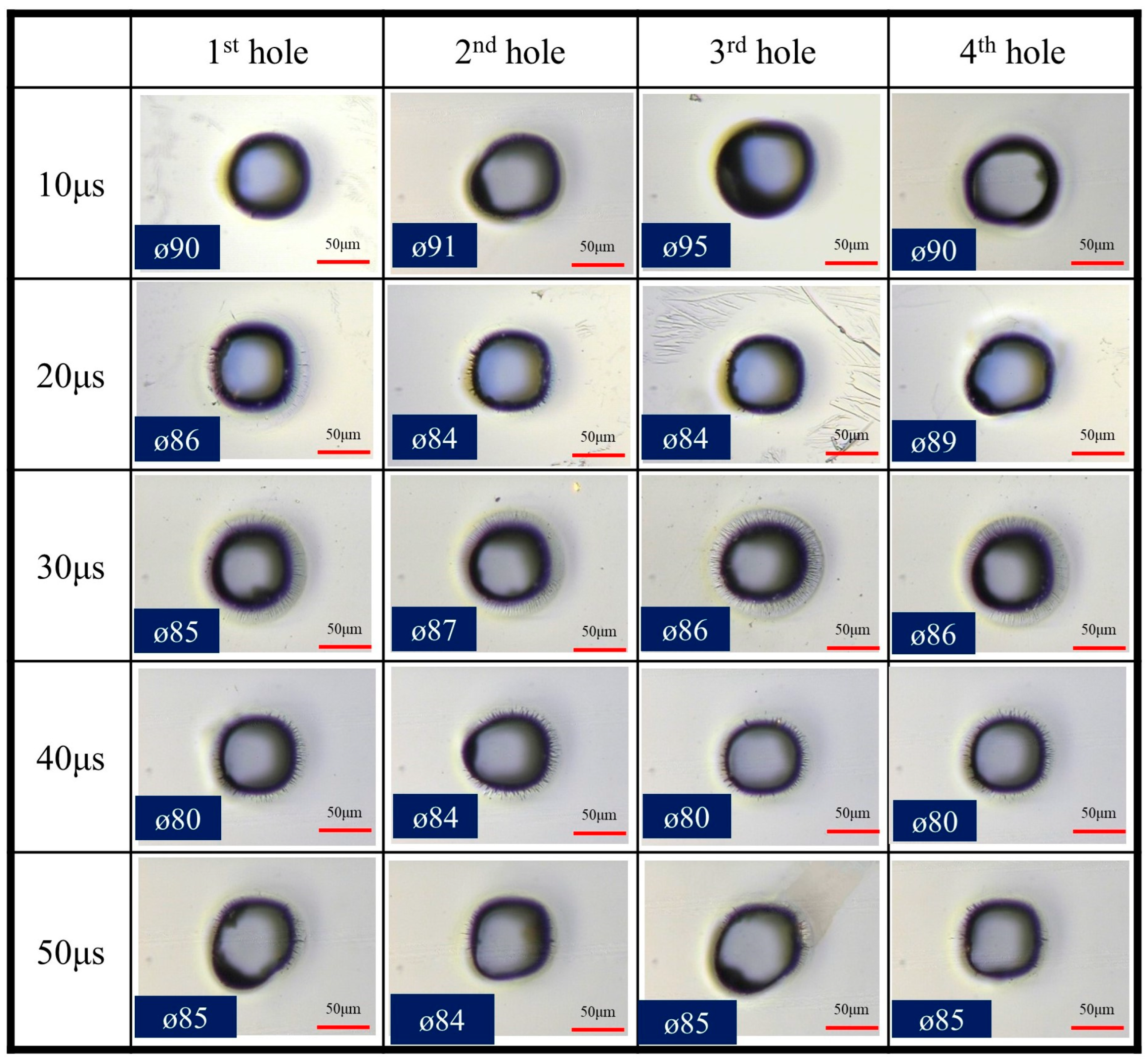
Figure 23 shows the inlet diameters and morphologies under different duration times. Figure 24 shows the outlet diameters and morphologies under different duration times. Under various duration time parameters, all the array micro-holes are free of outlet fragmentation, as shown in Figure 24. When the duration time is 40 μs, although the average inlet and outlet diameters meet the target dimensional accuracy, the average outlet diameter is 72.0 μm. This is too close to the lower limit of the target dimensional accuracy, so this parameter is not used.
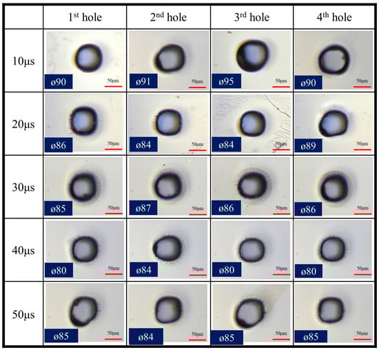
Figure 23.
The inlet hole morphology under different duration times.
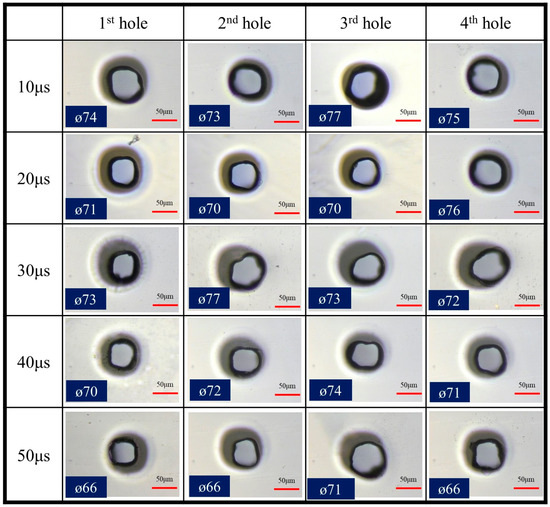
Figure 24.
The outlet hole morphology under different duration times.
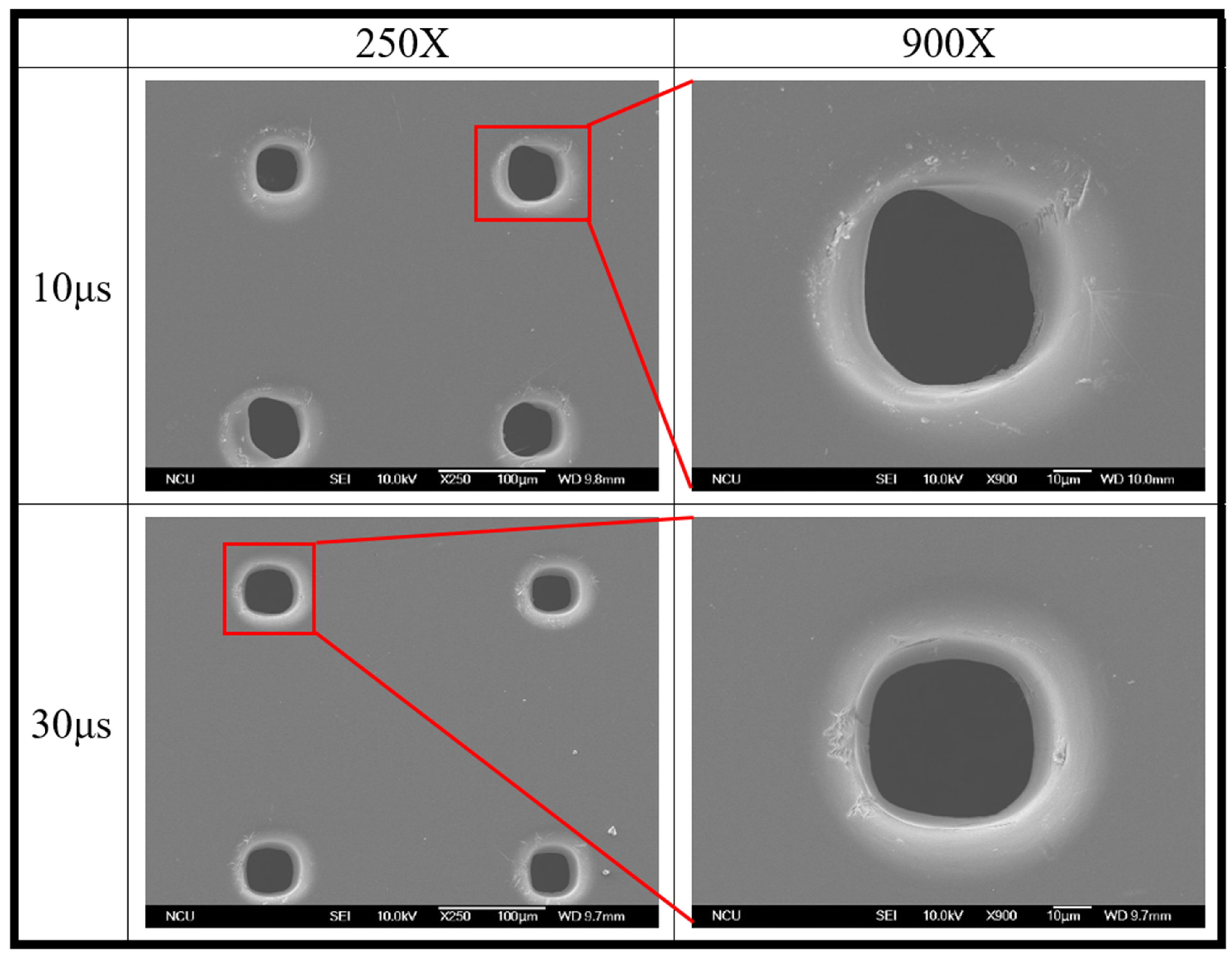
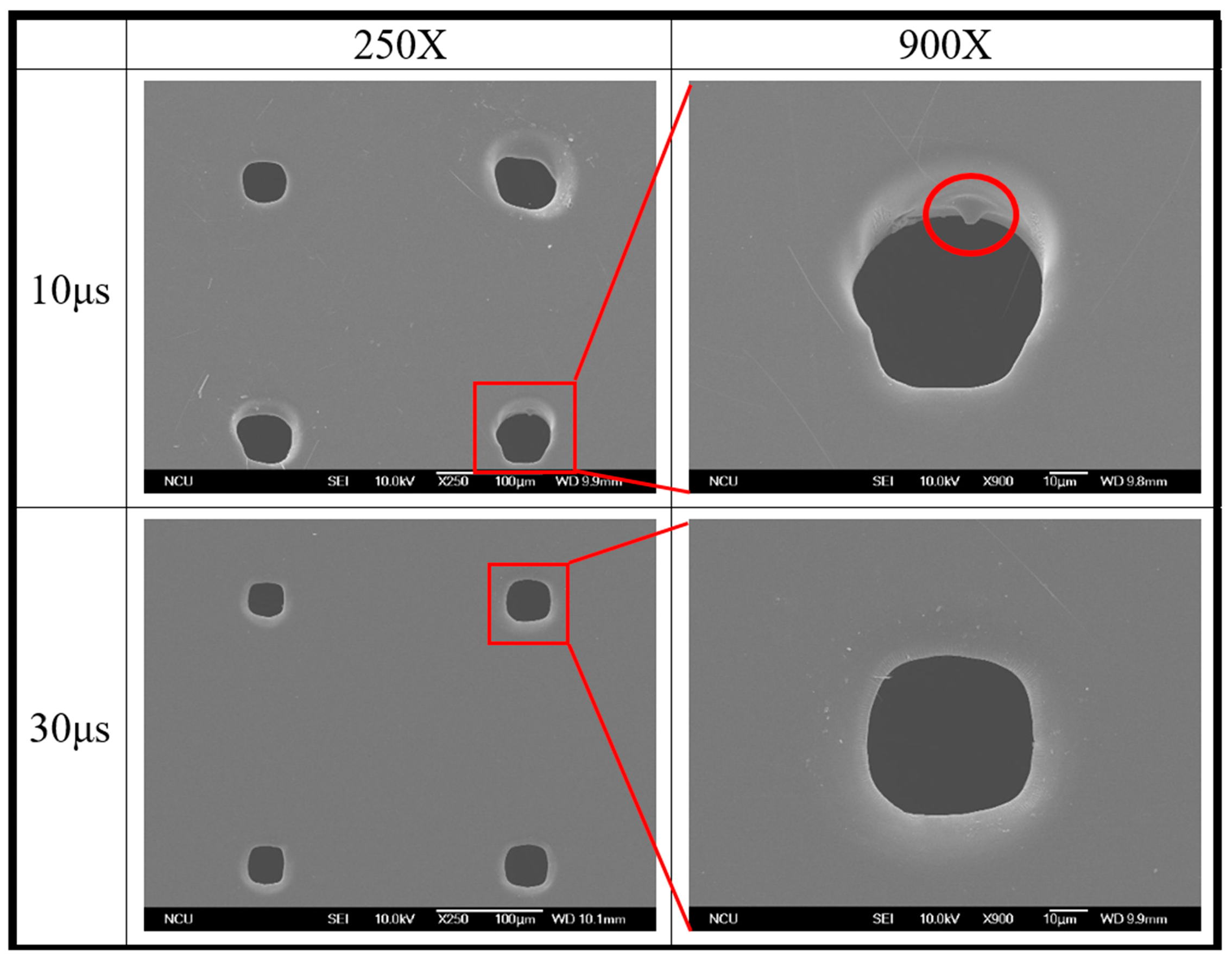
Figure 25 and Figure 26 show the SEM photos of the best and the worst inlet hole morphology under different duration times. According to the morphologies of the array micro-holes under the magnifications of 250 and 900 in Figure 25, when the duration time is 10 μs, the outline of the micro-holes is rough. According to the micro-hole outlet morphology in Figure 26, under the magnification of 250, the outline is rough. Under the magnification of 900, there is an unremoved part of the material, which is raised, as shown in the red circle in Figure 26. In contrast, the micro-hole morphology of the duration time of 30 μs is relatively smooth, and there is no material unremoved.
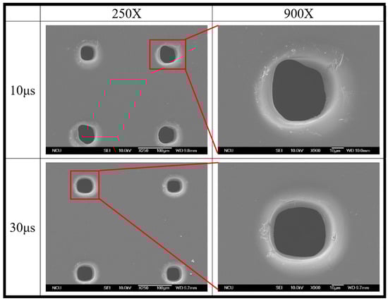
Figure 25.
The SEM photos of the worst (10 μs) and the best (30 μs) inlet hole morphology under different duration times.
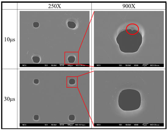
Figure 26.
The SEM photos of the worst (10 μs) and the best (30 μs) outlet hole morphology under different duration times.
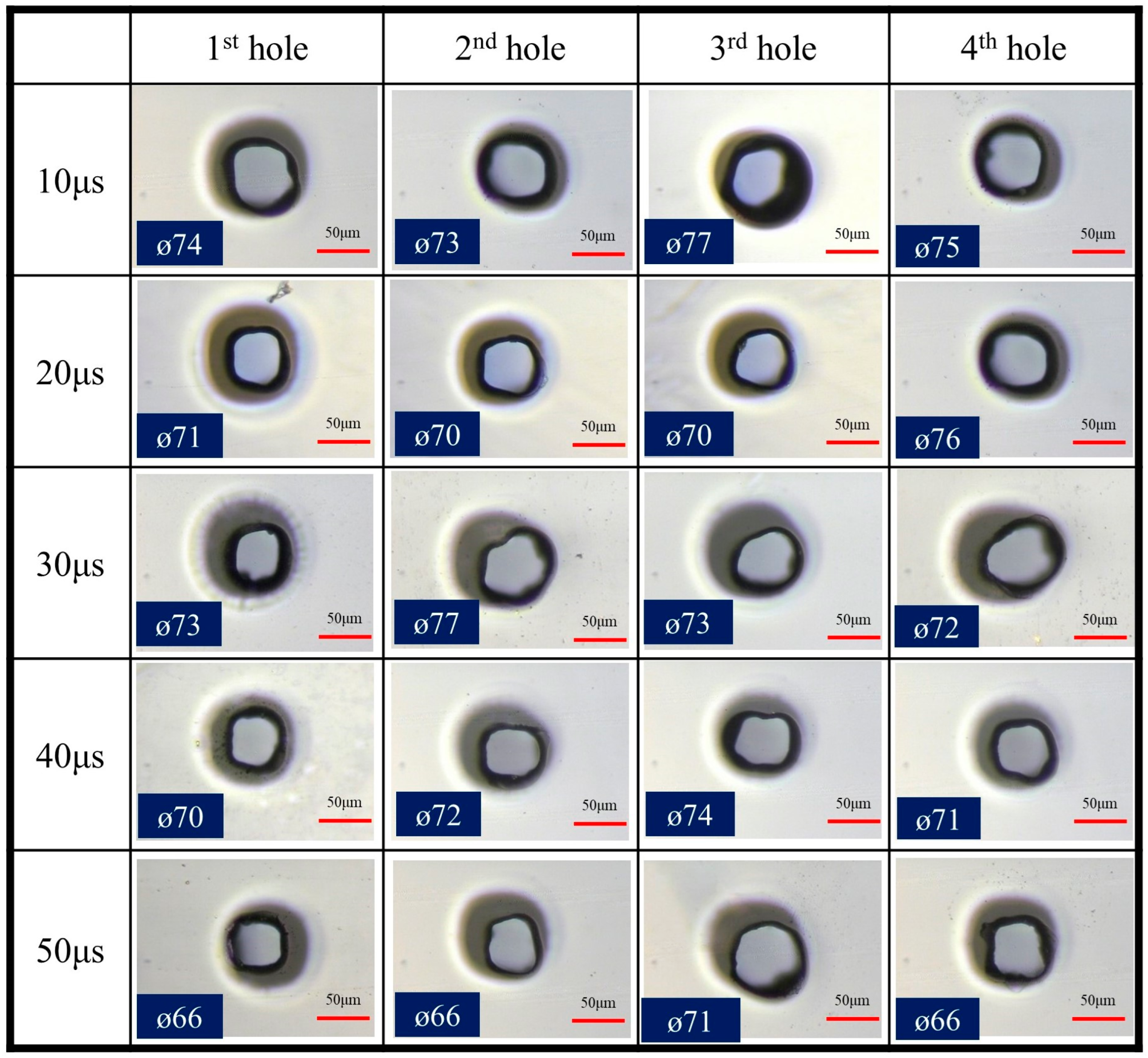
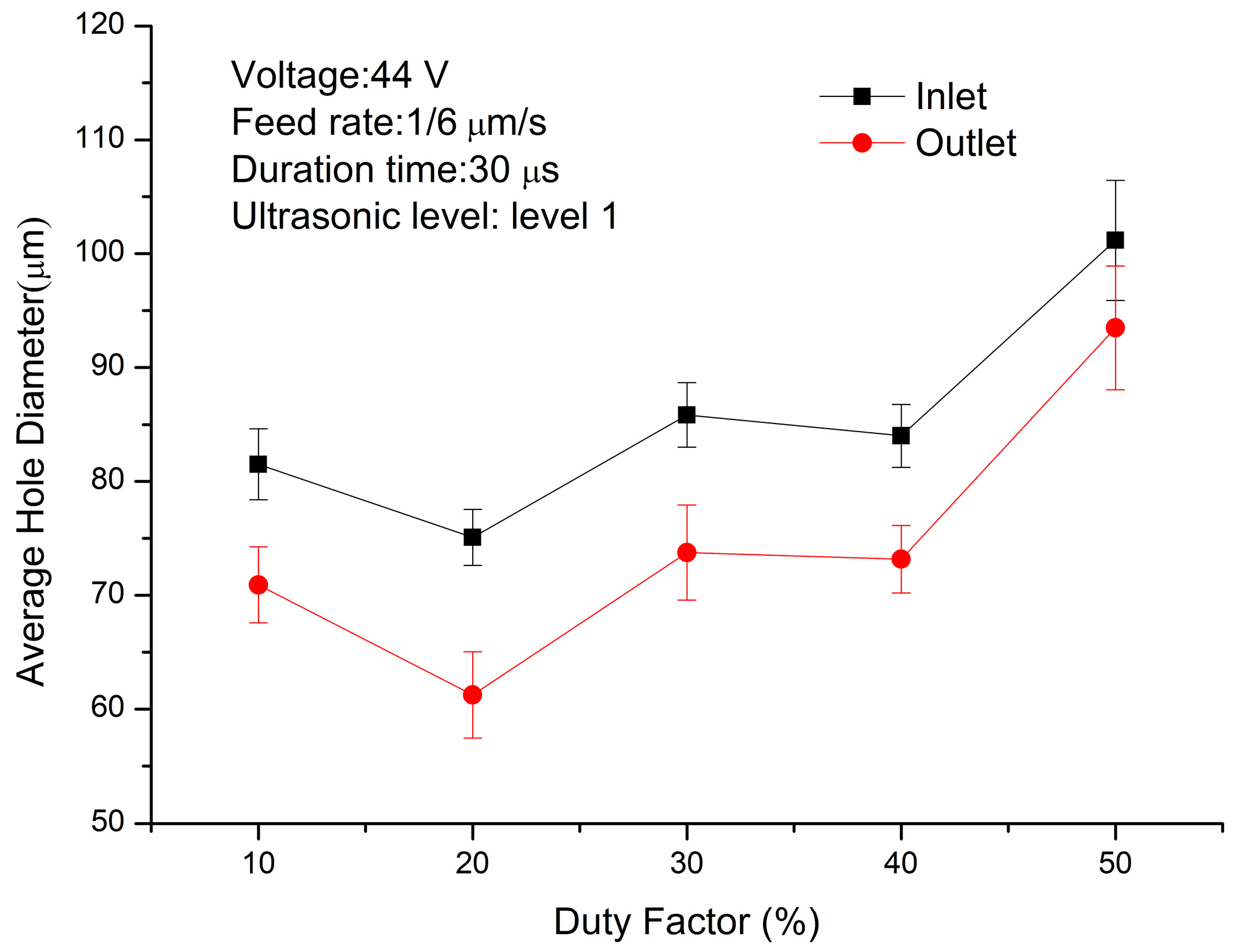
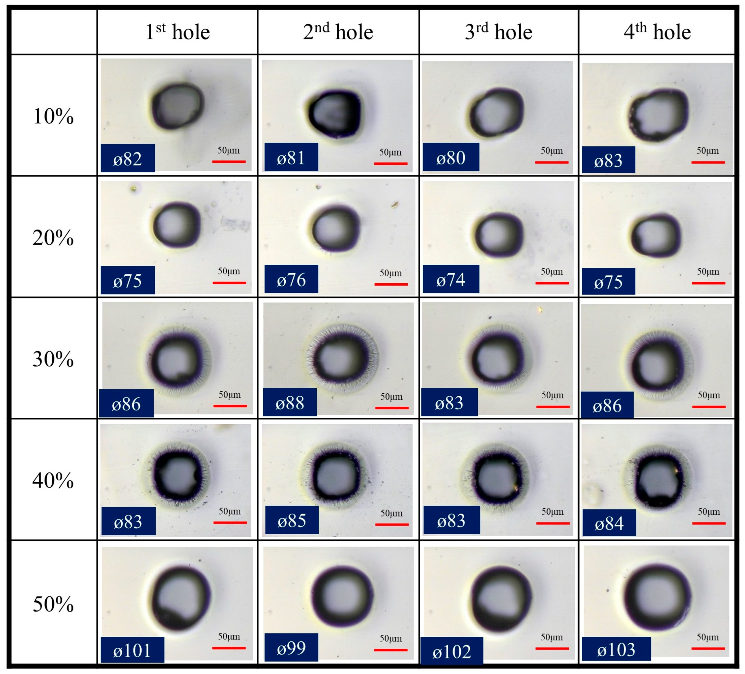
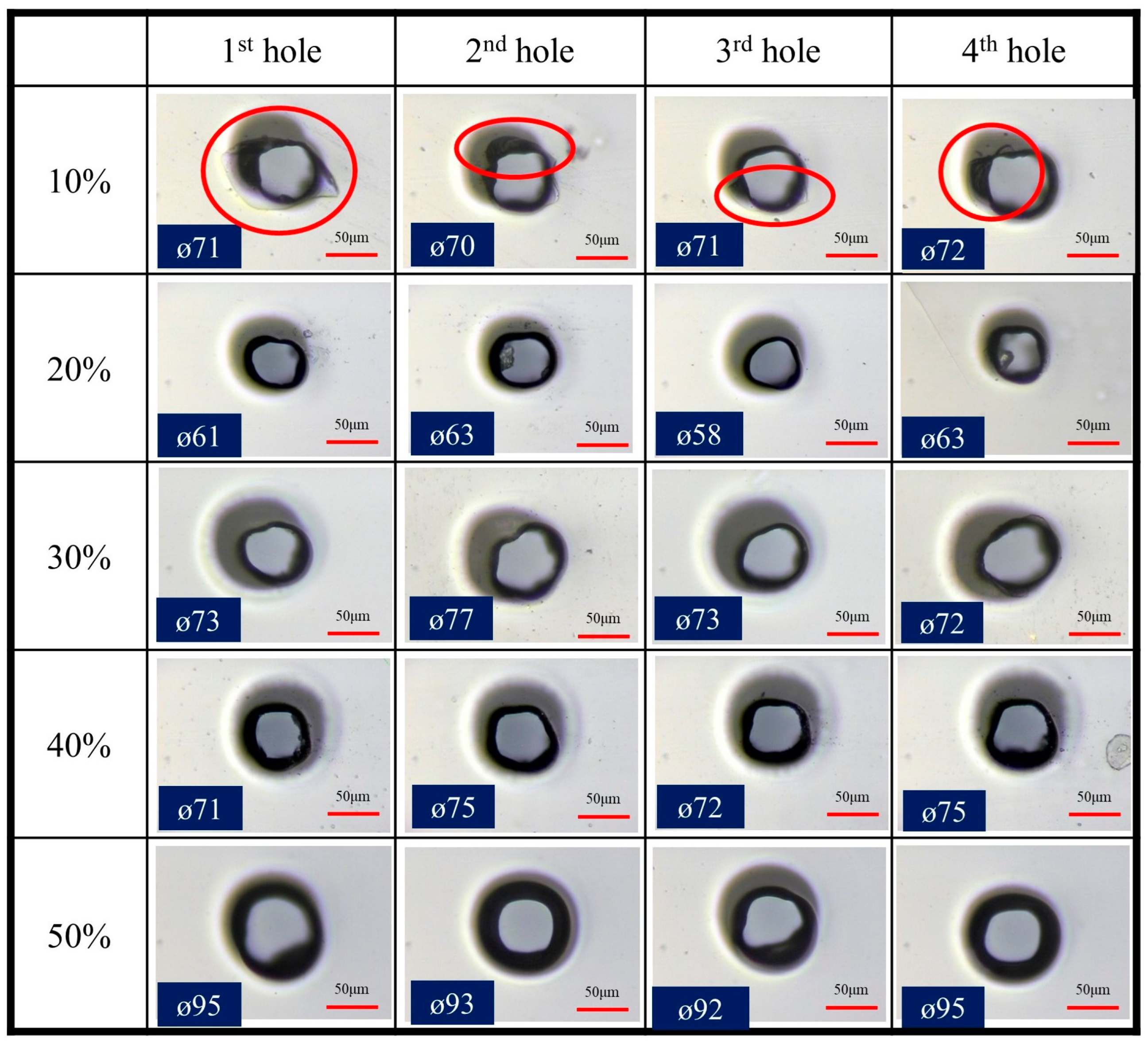
3.2.4. Effect of Duty Factor on Electrochemical Discharge Array Micro-Hole Machining
Figure 27 shows the relationships of the duty factor to the average inlet and outlet diameter. As the duty factor is increased from 10% to 20%, the average inlet diameter is decreased from 81.5 μm to 75.1 μm, and the average outlet diameter is decreased from 70.9 μm to 61.3 μm. As the duty factor is increased from 20% to 50%, the average inlet diameter is increased from 75.1 μm to 101.2 μm, and the average outlet diameter is increased from 61.3 μm to 93.5 μm. Because when the duty factor is 10%, the pulse-on time is too short, and the pulse-off time is long; the bubbles formed at the front end of the tool electrode during the pulse-on time are likely to separate from the surface of the tool electrode under the effect of buoyancy, and there is no time to form a dense insulating gas film. When the bubbles separate from the surface of the tool electrode, the tool electrode and the electrolyte are instantly connected to generate an electrolysis current phenomenon, leading to an increase in lateral discharge and insufficient axial processing capability. The bubbles separated from the surface of the tool electrode under the effect of buoyancy are likely to accumulate above the front end of the tool electrode. The lateral discharge is also increased, resulting in a large hole enlargement. Hence, the average inlet and outlet diameters when the duty factor is 10% are larger than the average inlet and outlet diameters when the duty factor is 20%, as shown in Figure 27. When the duty factor is large, as the discharge energy is increased, the hole enlargement phenomenon is more serious. When the duty factor is 30%, the average inlet diameter is 85.8 μm, and the average outlet diameter is 73.8 μm. When the duty factor is 40%, the average inlet diameter is 84.0 μm, and the average outlet diameter is 73.2 μm. Both of the duty factors of 30% and 40% can meet the target dimensional accuracy of 80 ± 8μm and are free of outlet fragmentation.
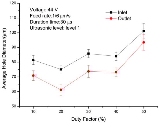
Figure 27.
The relationships of the average inlet and outlet diameters to the duty factor.
Figure 28 shows the inlet diameters and morphologies under different duty factors. Figure 29 shows the outlet diameters and morphologies under different duty factors. Because the pulse-on time is too short and the energy supply is insufficient, the axial processing capability is poor, resulting in the phenomenon of outlet fragmentation when the duty factor is 10%. Figure 29 shows the red circle of the duty factor of 10%. Both the duty factors of 30% and 40% meet the target dimensional accuracy. However, when the duty factor is 40%, observing the inlet morphology, the array micro-hole morphology at the inlet is relatively square, which is not as good as the approximately circular morphology when the duty factor is 30%.
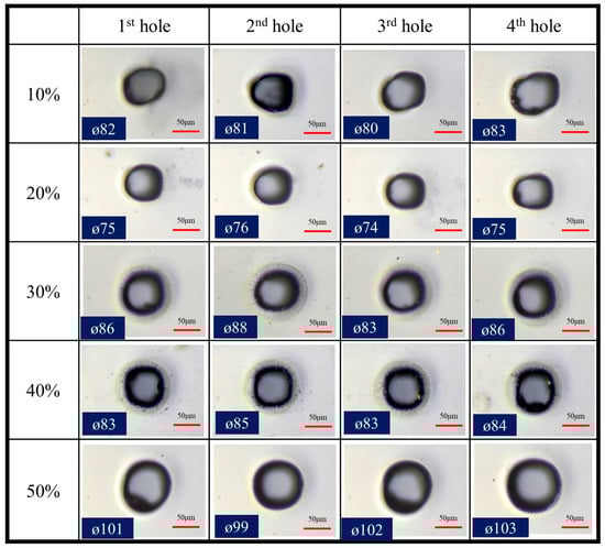
Figure 28.
The inlet hole morphology under different duty factors.
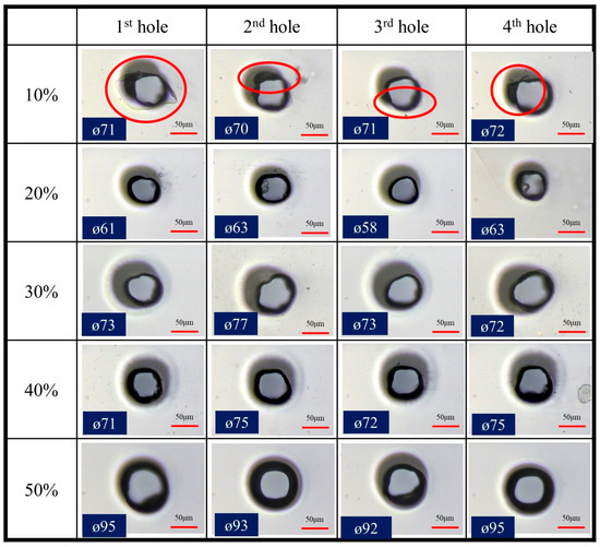
Figure 29.
The outlet hole morphology under different duty factors.
Figure 30 and Figure 31 show the SEM photos of the best and the worst inlet and outlet hole morphology under different duty factors. According to the morphologies of the array micro-holes under the magnifications of 250 and 900 in Figure 30, when the duty factor is 10%, the outline of the micro-holes is rough. According to the micro-hole outlet morphology in Figure 31, under the magnification of 250, there are multiple micro-hole outlet fragmentations, and the outline is rough, as shown in the red circle. Under the magnification of 900, the outlet fragmentation and the unremoved part of the material that is raised are observed, as shown in the red circle in Figure 31. In contrast, the micro-hole morphology when the duty factor is 30% is relatively smooth, and there is no material unremoved.
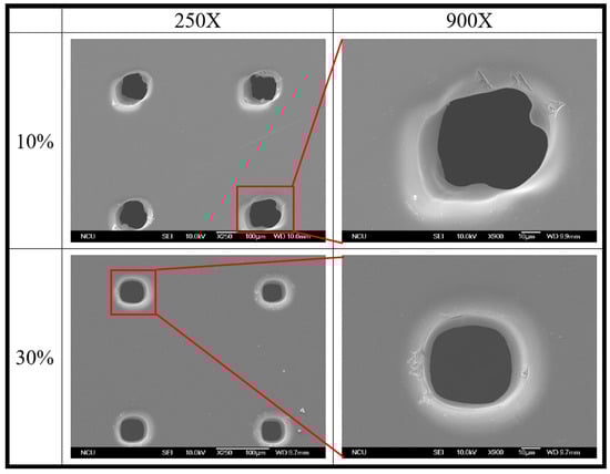
Figure 30.
The SEM photos of the worst (10%) and the best (30%) inlet hole morphology under different duty factors.
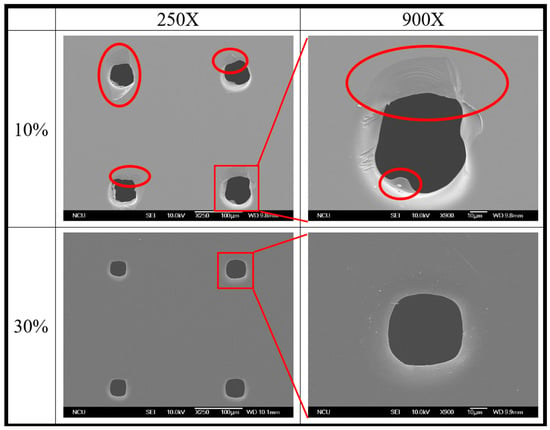
Figure 31.
The SEM photos of the worst (10%) and the best (30%) outlet hole morphology under different duty factors.
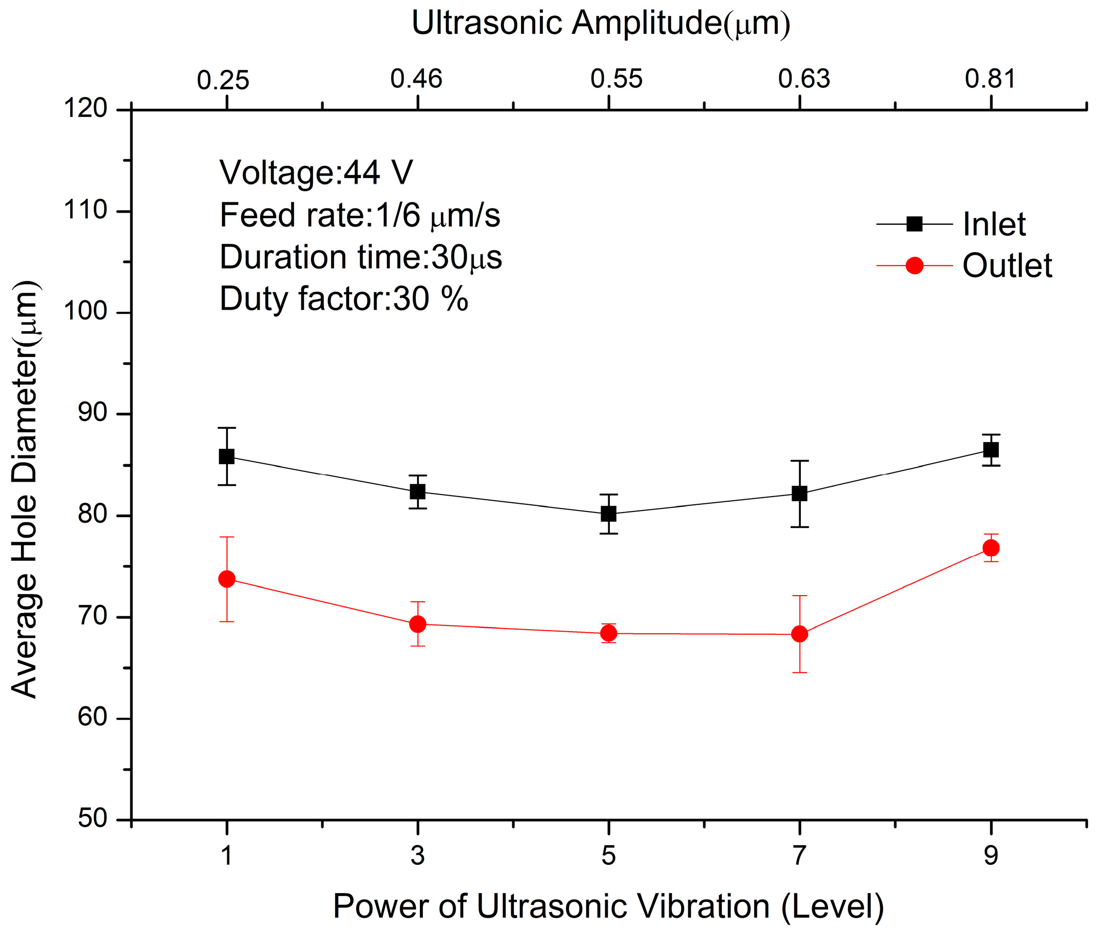
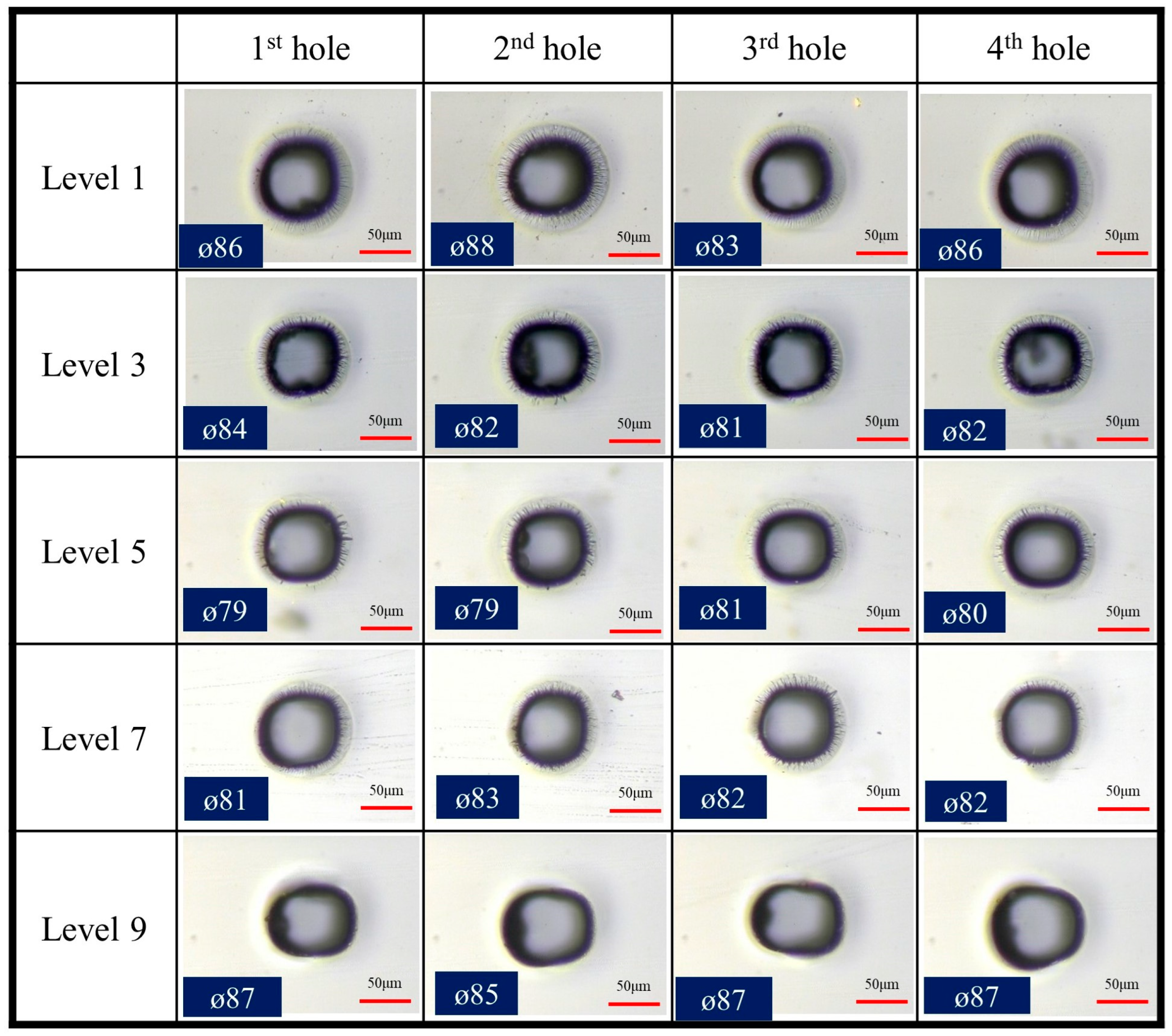
3.2.5. Effect of Ultrasonic Power Level on Electrochemical Discharge Array Micro-Hole Machining
The X-axis in the upper part of Figure 32 is the ultrasonic amplitude corresponding to each ultrasonic power level. The average inlet and outlet diameters are decreased as the ultrasonic power level is increased from Level 1 to Level 5, the average inlet diameter is decreased from 85.8 μm to 80.2 μm, and the average outlet diameter is decreased from 73.8 μm to 68.4 μm. As the ultrasonic power level is increased from Level 5 to Level 9, the average inlet diameter is increased from 80.2 μm to 86.5 μm, and the average outlet diameter is increased from 68.4 μm to 76.8 μm, as shown in Figure 32. The rapid up-and-down movement of the electrode can disperse excess bubbles in the ECDM process. The thinner insulating gas film leads to lower discharge energy and uniform discharge [11]. When the ultrasonic power level is Level 1, the ultrasonic vibration can thin the insulating gas film, but the ultrasonic amplitude is not large enough; the effect on thinning the insulating gas film is limited. When the ultrasonic power level is Level 5, the ultrasonic amplitude does not damage the stability of the insulating gas film, and the effect on thinning the insulating gas film is better. The hole enlargement is reduced, and the minimum average inlet and outlet diameters are obtained. When the ultrasonic power level is greater than Level 5, excessive ultrasonic amplitude excessively disturbs the insulating gas film, which is severely pulled up and down; the formation time of the insulating gas film is increased, and the distribution is uneven. When the insulating gas film is of uneven thickness, the critical voltage is variable. When the critical voltage is high, the hole enlargement is large [12].

Figure 32.
The relationships of the average inlet and outlet diameters to the ultrasonic power level.
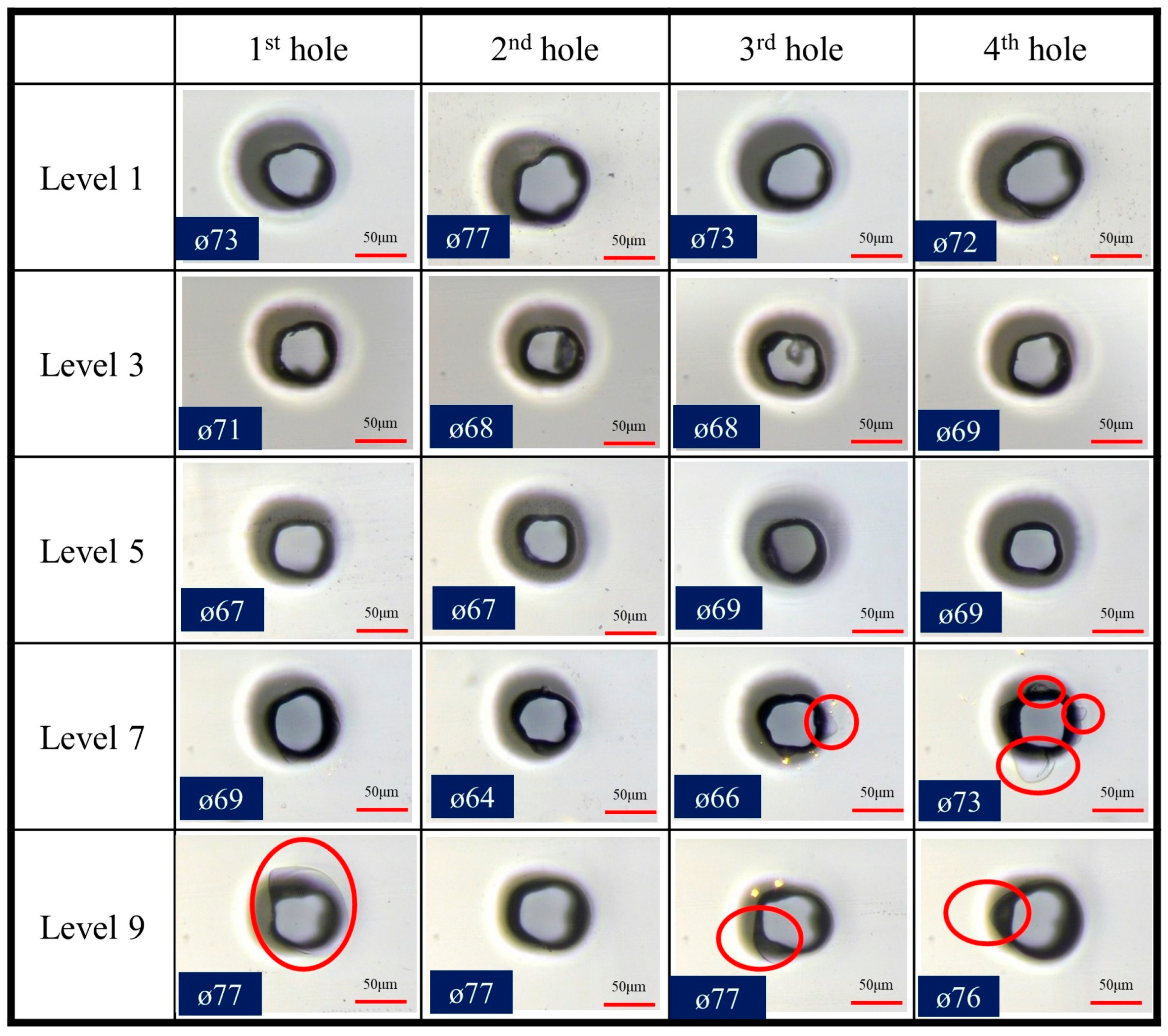
Figure 33 shows the inlet diameters and morphologies under different ultrasonic power levels. When the ultrasonic power level is Level 7 and Level 9, respectively, there is outlet fragmentation, as shown in the red circles of Figure 34, because the excessive ultrasonic amplitude destroys the stability of the insulating gas film. In particular, the insulating gas film at the front end of the tool electrode is incomplete, and the axial processing capability is poor, resulting in outlet fragmentation. The ultrasonic power of Level 1 and Level 9 meet the average inlet and outlet diameters of the target dimensional accuracy. However, there is outlet fragmentation when the ultrasonic power level is Level 9, so this parameter cannot be selected.
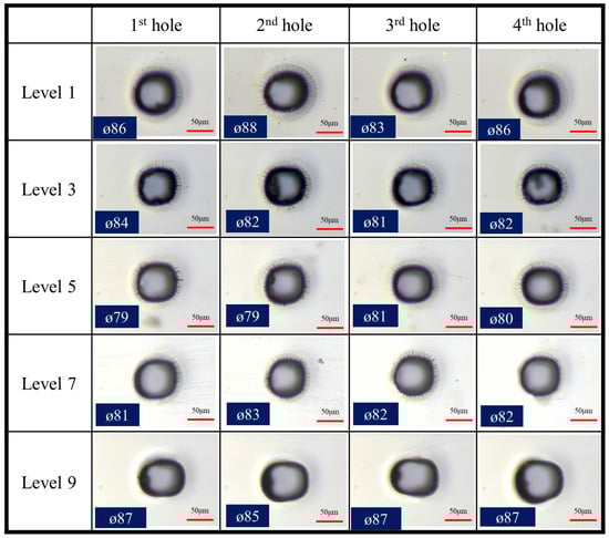
Figure 33.
The inlet hole morphology under different ultrasonic power levels.
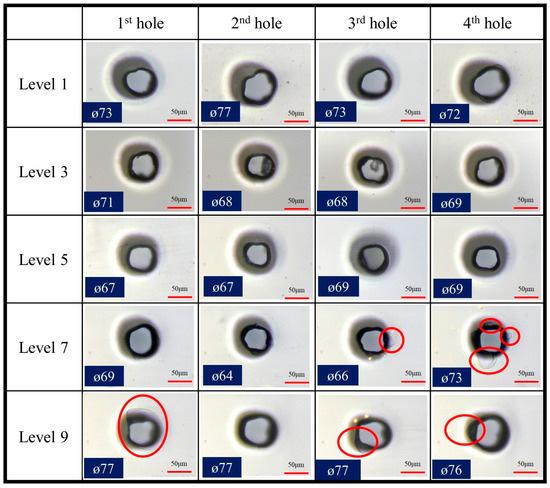
Figure 34.
The outlet hole morphology under different ultrasonic power levels.
Figure 35 and Figure 36 show the SEM photos of the best and the worst inlet and outlet hole morphology under different ultrasonic power levels. According to the morphologies of the array micro-holes under the magnifications of 250 and 900 in Figure 35, when the ultrasonic power level is Level 9, the outline of the micro-holes is rough. According to the micro-hole outlet morphology in Figure 36, under the magnification of 250, there are multiple micro-hole outlet fragmentations, and the outline is rough, as shown in the red circle. Under the magnification of 900, in addition to the outlet fragments, there is also a raised portion of material that has not been removed, as shown in the red circle in Figure 36. In contrast, the micro-hole morphology of the ultrasonic power Level 1 is relatively smooth, and there is no material unremoved. According to the experimental results, a working voltage of 44 V, feed rate of 1 μm/6 s, duration time of 30 μs, duty factor of 30%, and ultrasonic power level of 1 resulted in better inlet and outlet surface morphology. The combination of the parameters can also proceed without outlet fragmentation. Moreover, the average diameters of the inlet and outlet were roughly 80 μm while meeting the through-hole diameter of 80 μm with accuracy of ±8 μm.
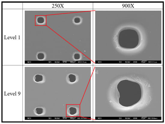
Figure 35.
The SEM photos of the best (Level 1) and the worst (Level 9) inlet hole morphology under different ultrasonic power levels.
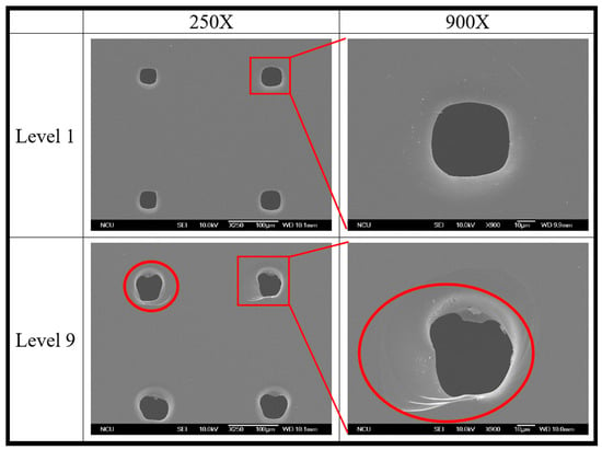
Figure 36.
The SEM photos of the best (Level 1) and the worst (Level 9) outlet hole morphology under different ultrasonic power levels.
4. Conclusions
This study used a pulse power supply and the assistance of ultrasonic vibration for the ECDM of quartz wafer array micro-holes. It also discussed the influence of various processing parameters on quality characteristics. The experimental results show that the ultrasonic vibration-assisted ECDM of array micro-holes can effectively improve the processing capability and outlet fragmentation, and better inlet and outlet array micro-hole surface morphologies are obtained. The target dimensional accuracy is achieved. The experimental results are concluded as follows:
- In terms of ECDM with and without the assistance of ultrasonic vibration, the assistance of ultrasonic vibration can thin the insulating gas film, making the insulating gas film thinner and more uniform. The processing performance is better, the workpiece rupture is improved, and the array micro-holes are processed on the quartz wafer successfully;
- In the ultrasonic vibration-assisted ECDM, the average inlet and outlet diameters can be increased simultaneously by increasing the working voltage. A high working voltage accelerates the bubble formation, a thick insulating gas film is formed, and the discharge energy is increased, resulting in a large hole enlargement;
- The average inlet and outlet diameters increase with the decrease in feed rate because at a low feed rate, the total processing time is relatively long, and the lateral discharging time is increased, resulting in a large amount of array micro-hole enlargement;
- A short duration of time forms a thick insulating gas film. In order to break through the thick insulating gas film, a high discharge energy is required, resulting in a large hole enlargement. Therefore, under different duration times, the average inlet and outlet diameters are increased as the duration time shortens;
- If the pulse-on time is too short and the pulse-off time is long, there is no time to form a dense insulating gas film, and the bubbles are likely to separate and accumulate at the upper edge of the front end of the tool electrode. Hence, the lateral discharge is increased, resulting in a large hole enlargement. Therefore, under different duty factors, the average inlet and outlet diameters are increased with the duty factor decreasing;
- Under different ultrasonic power levels, the average inlet and outlet diameters are decreased and then increased as the ultrasonic power level increases because the ultrasonic vibration can thin the insulating gas film, but the excessive ultrasonic amplitude excessively disturbs the insulating gas film, resulting in a large hole enlargement;
- According to the experimental results, the better parameter combination in this study comprises a working voltage of 44 V, feed rate of 1 µm/6 sec, duration time of 30 µs, duty factor of 30%, and ultrasonic power Level 1, and the average inlet and outlet diameters meet the target dimensional accuracy of 80 ± 8 µm. The average inlet diameter is 85.8 µm, and the average outlet diameter is 73.8 µm. There is no outlet fragmentation, and the morphology of the array micro-holes is better.
Author Contributions
Conceptualization, C.-H.Y. and H.-P.T.; methodology, C.-H.Y.; data curation, T.-C.W.; visualization, T.-C.W.; investigation, C.-H.Y. and H.-P.T.; supervision, J.-C.H. and H.-P.T.; writing—review and editing, C.-H.Y., J.-C.H. and H.-P.T.; writing—original draft preparation, T.-C.W. All authors have read and agreed to the published version of the manuscript.
Funding
This research was funded by National Science and Technology Council, project. No. 111WFA0710527.
Data Availability Statement
All data and materials during this study are included in this manuscript.
Acknowledgments
The authors gratefully acknowledge the funding support received from the National Science and Technology Council for funding the project. No. 111WFA0710527.
Conflicts of Interest
The authors declare no conflict of interest.
References
- Bhattacharyya, B.; Doloi, B.N.; Sorkhel, S.K. Experimental Investigations into Electrochemical Discharge Machining (ECDM) of Non-Conductive Ceramic Materials. J. Mater. Process. Technol. 1999, 95, 145–154. [Google Scholar] [CrossRef]
- Mochimaru, Y.; Ota, M.; Yamaguchi, K. Micro Hole Processing Using Electro-Chemical Discharge Machining. J. Adv. Mech. Des. Syst. Manuf. 2012, 6, 949–957. [Google Scholar] [CrossRef]
- Singh, T.; Dvivedi, A. Impact of Gas Film Thickness on the Performance of RM-ECDM Process during Machining of Glass. Mater. Manuf. Process. 2022, 37, 652–663. [Google Scholar] [CrossRef]
- Arab, J.; Adhale, P.; Mishra, D.K.; Dixit, P. Micro Array Hole Formation in Glass Using Electrochemical Discharge Machining. Procedia Manuf. 2019, 34, 349–354. [Google Scholar] [CrossRef]
- Rusli, M.; Furutani, K. Performance of Micro-Hole Drilling by Ultrasonic-Assisted Electro-Chemical Discharge Machining. Adv. Mater. Res. 2012, 445, 865–870. [Google Scholar] [CrossRef]
- Elhami, S.; Razfar, M.R. Effect of Ultrasonic Vibration on the Single Discharge of Electrochemical Discharge Machining. Mater. Manuf. Process. 2018, 33, 444–451. [Google Scholar] [CrossRef]
- Zheng, Z.-P.; Lin, J.-K.; Huang, F.-Y.; Yan, B.-H. Improving the Machining Efficiency in Electrochemical Discharge Machining (ECDM) Microhole Drilling by Offset Pulse Voltage. J. Micromech. Microeng. 2008, 18, 025014. [Google Scholar] [CrossRef]
- Wüthrich, R.; Fascio, V. Machining of Non-Conducting Materials Using Electrochemical Discharge Phenomenon—An Overview. Int. J. Mach. Tools Manuf. 2005, 45, 1095–1108. [Google Scholar] [CrossRef]
- Rathore, R.S.; Dvivedi, A. Sonication of Tool Electrode for Utilizing High Discharge Energy during ECDM. Mater. Manuf. Process. 2020, 35, 415–429. [Google Scholar] [CrossRef]
- Han, M.-S.; Min, B.-K.; Lee, S.J. Geometric Improvement of Electrochemical Discharge Micro-Drilling Using an Ultrasonic-Vibrated Electrolyte. J. Micromech. Microeng. 2009, 19, 065004. [Google Scholar] [CrossRef]
- Yang, C.-H.; Tsui, H.-P. Study on Ultrasonic-Assisted WECDM of Quartz Wafer with Continuous Electrolyte Flow. Int. J. Adv. Manuf. Technol. 2022, 118, 1061–1076. [Google Scholar] [CrossRef]
- Chen, Y.; Feng, X.; Xin, G. Experimental Study on Ultrasonic Vibration-Assisted WECDM of Glass Microstructures with a High Aspect Ratio. Micromachines 2021, 12, 125. [Google Scholar] [CrossRef] [PubMed]


Disclaimer/Publisher’s Note: The statements, opinions and data contained in all publications are solely those of the individual author(s) and contributor(s) and not of MDPI and/or the editor(s). MDPI and/or the editor(s) disclaim responsibility for any injury to people or property resulting from any ideas, methods, instructions or products referred to in the content. |
© 2023 by the authors. Licensee MDPI, Basel, Switzerland. This article is an open access article distributed under the terms and conditions of the Creative Commons Attribution (CC BY) license (https://creativecommons.org/licenses/by/4.0/).