Article

A Low-Cost Drive and Detection Scheme for Electrowetting Display

1
College of Information Science and Technology, Zhongkai University of Agriculture and Engineering, Guangzhou 510225, China
2
Intelligent Agriculture Engineering Research Center of Guangdong Higher Education Institutes, Zhongkai University of Agriculture and Engineering, Guangzhou 510225, China
3
Institute of Electronic Paper Displays, South China Academy of Advanced Optoelectronics, South China Normal University, Guangzhou 510006, China
*
Author to whom correspondence should be addressed.
Processes 2023, 11(2), 586; https://doi.org/10.3390/pr11020586
Submission received: 15 January 2023 / Revised: 11 February 2023 / Accepted: 12 February 2023 / Published: 15 February 2023
(This article belongs to the Special Issue Processes in Electrical, Electronics and Information Engineering)

Abstract

:
The electrowetting display (EWD) has obtained much attention as its readability in sunlight and flexible displays. Oil motion control is an important factor for the display performance of EWD. In this paper, we propose a low-cost drive and detection scheme for EWD. The dynamic drive and detection scheme for EWD consists of a low-cost camera, computer and graphical detection system, and portable driving control system. The proposed scheme can detect oil leaking, splitting, and non-recovered defects successfully. Moreover, surface defects such as the hydrophobic layer burned and scratch can also be captured and analyzed by the proposed scheme. We hope that this scheme can provide a drive and detection platform for other EWD researchers.

1. Introduction

Emissive display technologies (e.g., Liquid crystal display) still dominate the display field and related industries. However, in recent years, various reflective display technologies have developed rapidly. Among these reflective display technologies, the characteristics of the electrowetting display (EWD) are the most obvious. The Electrowetting principle was first published in 1981 [1]. After that, Hayes demonstrated the use of electrowetting as a principle for a reflective display [2]. The advantages of EWD mainly include a flexible display, low power consumption, and fast response [3].
Previous research for EWD has mainly focused on dielectric layer materials [4], pixel structures [5,6], and driving waveform [7,8]. The research on the accurate control of oil movements is relatively few [9]. Li Wei’s team studied the charge trapping and oil backflow problem in EWD devices and proposed a quick response driving scheme [10]. However, EWD products still have some issues to overcome in the current. Oil motion defects such as oil leaking, splitting, and non-recovered are observed and captured in a large number of experiments [11].
Therefore, in a previous study [12,13,14], monitoring the oil motion status of an EWD device is often performed manually. However, high-reliability products are the key to the industrialization of EWD. In the progress of product development, the defects detection and classification system can effectively find root causes of failure and shorten production time. Therefore, a reliable and intelligent drive and detection scheme for EWD devices should be proposed and developed if necessary.
At present, the mature EWD device detection scheme is the equivalent capacitance-based method [15,16]. The pixel unit of the EWD device can be regarded as a “capacitor”. The change in oil motion will lead to the change in the equivalent capacitance at both ends of the pixel unit. The control system can detect the state of the pixel unit by continuously collecting and observing the change in the equivalent capacitance value. The detection scheme based on equivalent capacitance can effectively detect EWD defects such as non-ideal oil motion and conductive damage. However, this scheme requires a large number of sensors, the detection speed is slow, and it is difficult to detect small defects such as scratches and oil splitting.
In this paper, we propose a low-cost drive and detection scheme for EWD. It is composed of an EWD device, a low-cost camera, a computer, and graphical detection system and portable driving control system. This scheme can detect several EWD defects caused by oil motion and degradation of hydrophobic layers due to multiple drives.
Section 2 describes the relevant principle of EWD. Section 3 presents the details of the proposed drive and detection scheme. Section 4 gives the different experiment results, analysis, and discussion. Finally, our conclusions are given in Section 5.

2. Electrowetting Display Structure and Display Principle

The EWD pixel structure and display principle [17] are shown in Figure 1. An EWD pixel is composed of a transparent electrode, an insulator layer, a hydrophobic layer, a colored oil layer, water, and a hydrophilic grid (as a pixel wall).
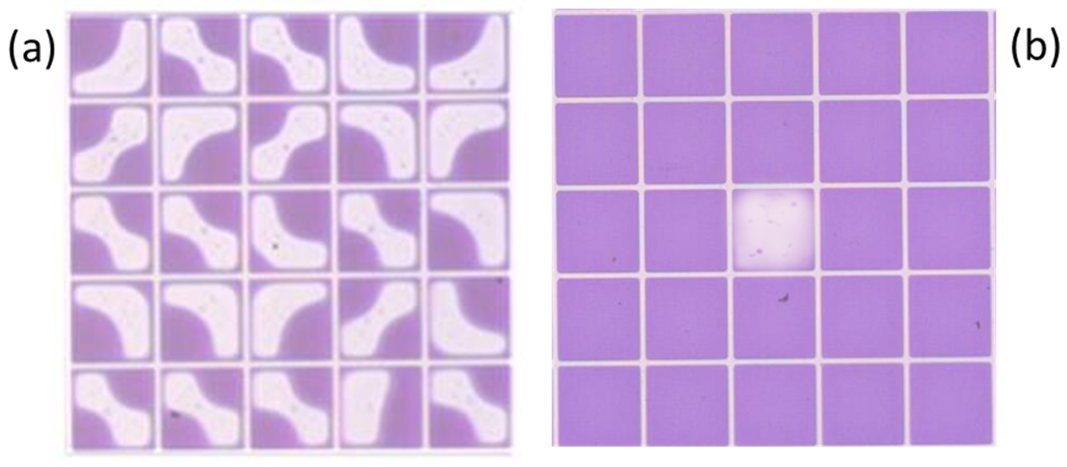
As Figure 1a shows, if a sufficient external voltage is not applied, the black oil-absorbing light will be completely laid on the surface of the hydrophobic layer. Therefore, the light cannot pass through. In this case, the pixel is off and black. When we give enough voltage (Generally speaking, above 20 V) on the EWD pixel, as shown in Figure 1b, the incident light from the top penetrates the whole pixel and reflects back from the bottom reflection layer. So, in this case, the pixel is on and white. However, previous studies have found that the oil is distributed in the four corners of the pixel unit. The reason for this is that the higher the voltage applied to the film, the stronger instability is generated, and the shorter the rupture time is [18,19]. Figure 2a shows the oil-splitting phenomenon in the EWD pixel. We can see that the oil distribution in the EWD pixel is random and shows various shapes.
In addition, previous research [20] found that the oil will jump out of the pixel due to improper driving waveforms or errors in the manufacturing process, as shown in Figure 2b. This phenomenon is called oil leaking.

3. Proposed Drive and Detection Scheme for EWD

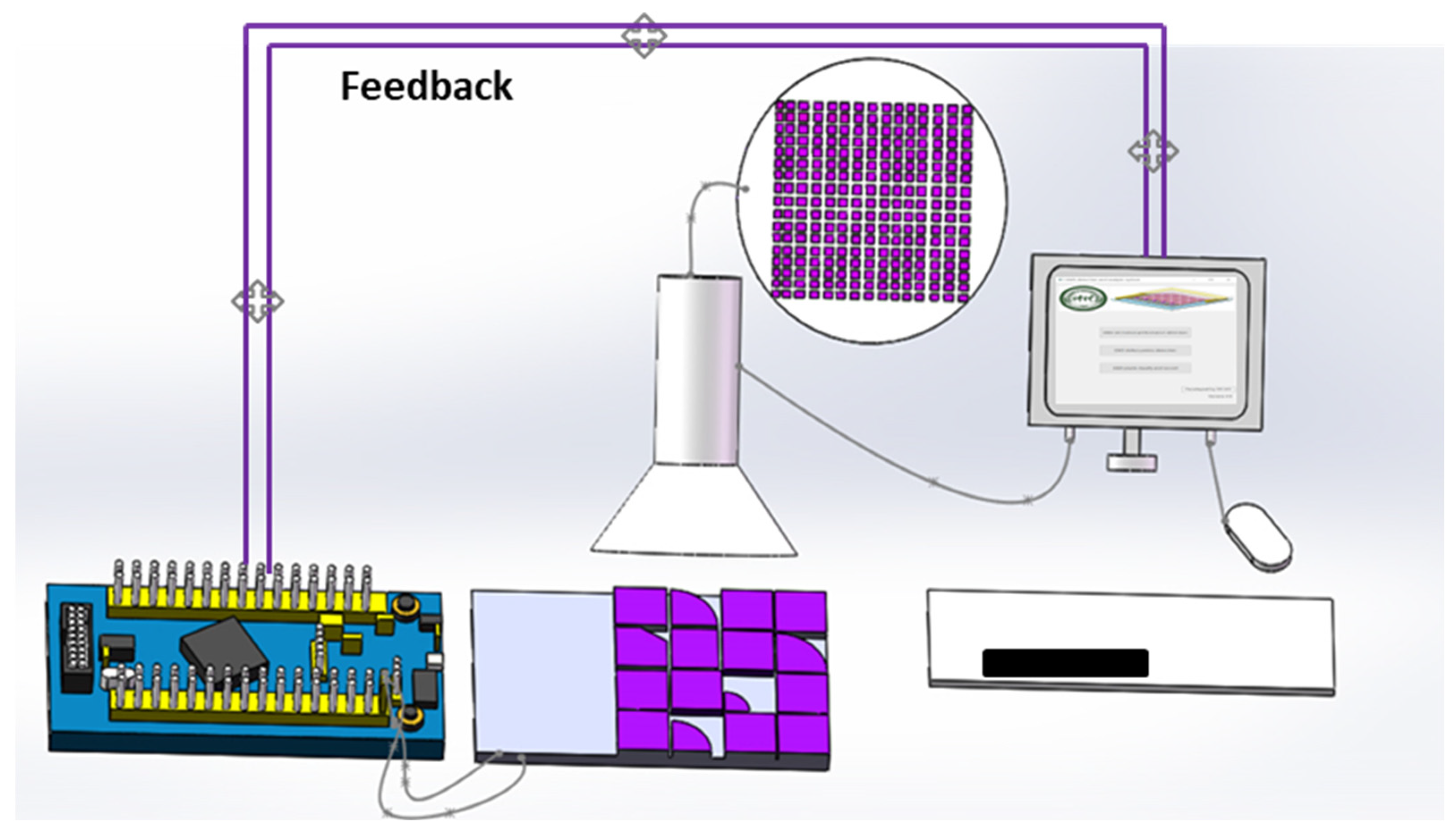
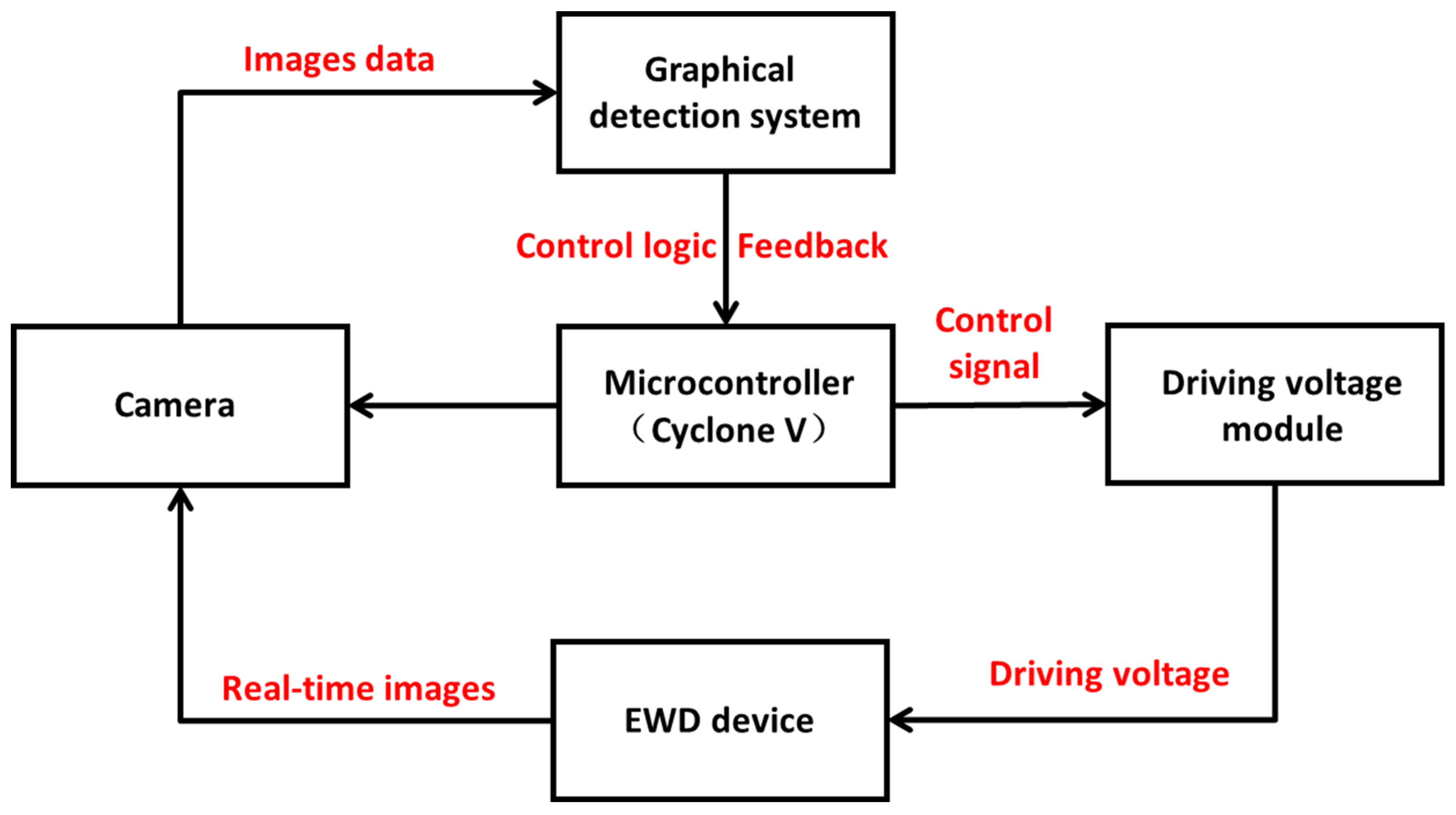
The 3D schematic diagram of the drive and detection scheme for EWD is shown in Figure 3. The dynamic drive and detection scheme for EWD proposed in this paper consists of the EWD device: a low-cost camera (Resolution:  1292 × 964 , FPS: 30, pixel size:  3.75 × 3.75   μ m , interface: GigE), computer and graphical detection system, and portable driving control system. Figure 4 gives the block diagram of the detection and feedback mechanism.
The feedback signal (detection results) processed by the image analysis system is transferred to the control core. Moreover, the image analysis system displays the detection and classification results. The detailed description of the drive and detection scheme for EWD is elaborated in the following subsections.

3.1. EWD Device Fabrication

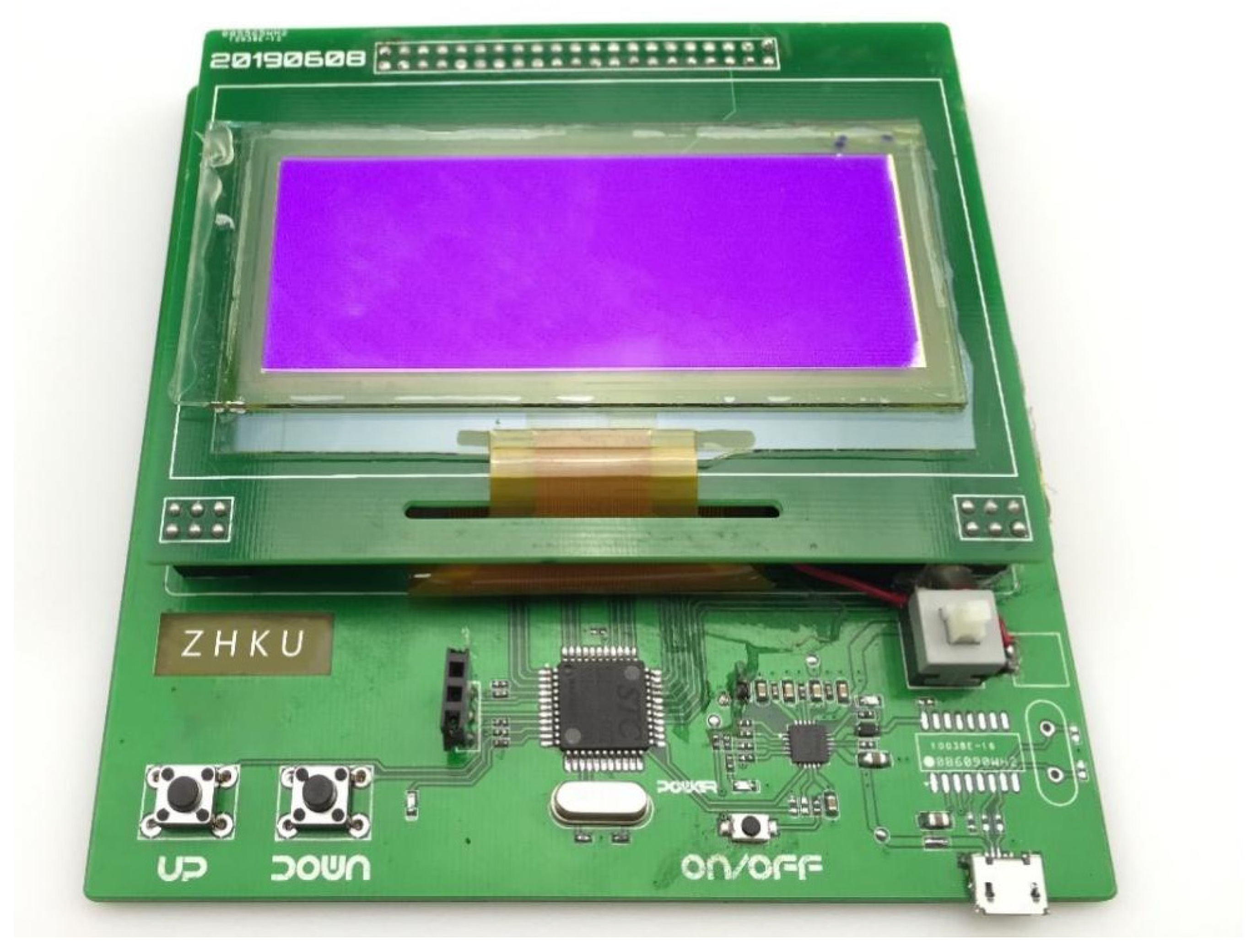
Figure 5 provides the physical picture of the EWD chip and the supporting driving system. EWD pixel fabrication begins with indium tin oxide sputter deposition onto the glass substrate. The shape and size of the pixels were realized on the lower substrate by photolithography. Following, we spun a coat of 1000 nm Teflon Amorphous Fluoropolymer-1600 on the lower substrate as a hydrophobic layer. The pixel wall is made of a SU-8 photoresist. In our EWD devices, the height of the pixel is 6 μm, and the width is 15 μm. We inject enough alkane-colored (purple) oil into every EWD pixel unit through the self-assembly method. Finally, the ITO cover plate with a pressure-sensitive adhesive (PSA) edge seal was used as the upper substrate of the EWD chip.
To ensure the different signal interaction between the EWD chip and external driving voltage module, a printed circuit board (PCB) foil was designed. Each pixel unit of the EWD chip was controlled by an independent electrical connector. In this way, the external driving control system could turn on or off each pixel unit of the EWD chip separately.

3.2. Machine Vision-Based EWD Detection System

The capacitance-based method is a mature detection method for EWD. It is easy to implement. However, this scheme requires a large number of sensors, and the detection speed is slow. The machine vision-based detection system EWD device was presented in this work. Compared with the former, the proposed scheme is more accurate and can detect more defects (e.g., surface defects, oil leaking). There are two types of defects that can be identified by the machine vision-based EWD detection system. One is the oil motion defect the other is the surface defect damaged in the manufacturing process or driving process.
EWD image data collection, EWD image processing, EWD defects recognition and classification, and feedback are the four most important steps of the proposed detection scheme. In this study, we developed a complete image recognition scheme for the two types of defects of the EWD chip. The image recognition and analysis solution of the whole process for oil motion performance is shown in Figure 6a.
First, the camera collects the original image of the EWD device at a rate of 30 frames per second. The K-nearest neighbor (KNN) background model of the original image is built by the detection system. To eliminate salt-and-pepper noise in the EWD image, we also developed a median-based Gaussian weighted filter (MGWF) that was effective for image edge filtering. The MGWF algorithm proposed in this paper uses a weighted operator to weigh the signal pixels in the image of the EWD device and then outputs the weighted median value. The MGWF algorithm can more accurately distinguish the noise and signal pixels in the image of the EWD device. This operation can obtain better de-noising performance and edge detail retention ability. For fluid-driven devices such as EWD, the visualization of EWD device images can be significantly improved.
Then, we use the adaptive algorithm provided by the OpenCV library to process the image and traverse all the points on the region of interest (ROI). Finally, the aperture ratio was obtained by analyzing and calculating the ROI. In addition, the system displays the oil motion defects detection results based on custom taxonomy.
The identification scheme and process of surface defects are shown in Figure 6b. In this solution, morphology processing is developed and carried out on the binary image obtained from the previous step. The image inflation and image corruption algorithm are used to reduce image noise. Here, we also used MGWF, which is effective for defect edge filtering. A canny edge recognition algorithm was used to detect the edge of the EWD defect in this study. The Canny algorithm has a good signal-to-noise ratio. It is widely used in the edge detection of fluid images. It includes the following steps:
  • Use the first-order partial derivative of the Gaussian function to calculate the gradient and detect the local maximum of the gradient modulus;
  • Use a low threshold to obtain the weak edge of the EWD defect image and use a high threshold to obtain the strong edge of the EWD defect image; obviously, the weak edge contains a strong edge at this time;
  • Take the connected components in the weak edge that are associated with the strong edge as the output edge.
Finally, the surface defects detection result of the EWD device is obtained and displayed on a graphical user interface (GUI).

3.3. Driving Control System

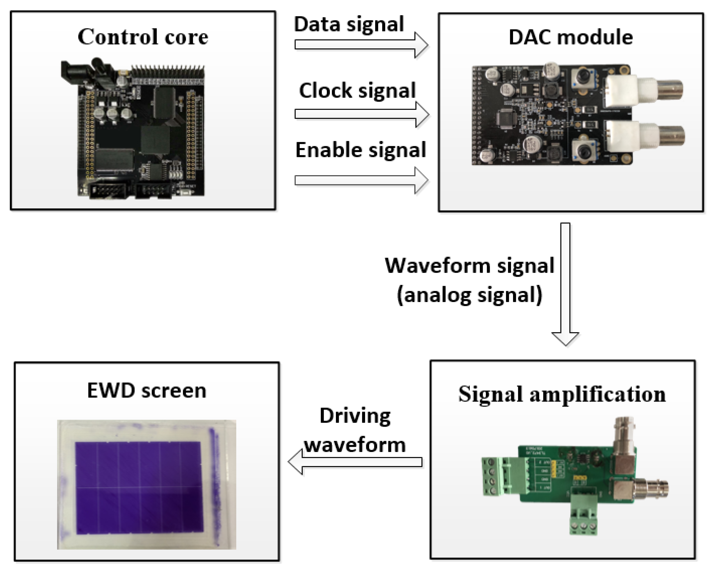
A portable and programmable EWD driving control system was presented to realize the control of the EWD device. The logic control unit, digital-analog conversion (DAC) unit, and voltage amplification unit are the three major components of the driving control system. Figure 7 is the system module diagram of the proposed driving control system.
The field programmable gate array (FPGA, Cyclone V) was used for the control unit in our study to realize the EWD device control. The logic control unit is to realize the EWD control logic, including device display timing and waveform editing.
The workflow of the driving control system is given in Figure 8. First of all, the system programs all the bytes of the SRAM with the firmware after power-on. All of the driver and communication-related registers are initialized and configured. Then, the driving control system establishes a connection with the EWD detection system on the PC.
Next, the driving control system stays on standby until the user enters the control command. The system writes corresponding data to the corresponding control register after the control command has been received. Subsequently, the driving waveform is generated and output to the pixel unit of the EWD device.
The output of the logic control unit is in the form of a digital signal. Therefore, we need to convert it into an analog signal. In our system, we used AD9767 to realize the DAC of the data. It should be mentioned that the output of the AD9767 chip is in the form of a current. In order to meet the high voltage-driven characteristics of the EWD chip, a voltage amplification unit with three-stage amplification is presented and developed to convert and amplify the current signal of the upper output. Table 1 shows the output format of each control unit. The EWD device obtains the required high-voltage driving signal, which is then processed by the above units.
The driving control system is designed and developed to manage a series of driving logic and control timing for the EWD chip. In order to improve the operability of the system, we developed a serial interactive module between the drive control system and the graphical detection system. The experimenter can conveniently edit and control the driving waveform in the graphical detection system.

4. Results and Discussion

It can be seen from the experiment that different oil motion defects were observed when an inappropriate voltage signal was applied to the EWD device. For the EWD device, the aperture ratio in an EWD pixel can be defined as:
Aperture   ratio   ( % ) = ( 1   A o i l A p i x e l ) × 100 %
where  A o i l  and  A p i x e l  denote the pixel area occupied by the oil and the overall area of the pixel at some point, respectively. In this study, the calculation of the pixel aperture ratio ignored the area of the pixel wall.

4.1. The Output Verification of Drive Control System

The driving control system is one of the key modules of the EWD system. Thus, we first verify the proposed drive control system before the detection experiments of the EWD device. The purpose of this is to ensure that the driving waveform output by the control system meets the requirements of the EWD device.
In this section, we compared our driving control system with a standard waveform generator. Both of them generate the same driving waveform (shown in Figure 9a) on the same EWD device. The microscope with the CCD camera is used to analyze the display results manually. The experimental results (Figure 9b) show that the output error of the proposed scheme is about 3 ms in the open state of the EWD device. The reason for this is that it takes time for the control core to output the data signal to the driver chip. Additionally, the generation of corresponding high voltage has a preparation stage. In addition, the difference between them is only about 1 ms in the close state of the EWD device. Overall, the error of both of them (the proposed scheme and waveform generator) is less than 5%.

4.2. The Aperture Ratio of EWD Pixel Detection

In this section, we use the proposed scheme to detect the aperture ratio of an EWD pixel unit from the closed state to the fully open state. This experimental purpose verifies the real-time, and reliability of the proposed scheme. In this experiment, we observed and recorded the oil movement state in the EWD pixel unit by the proposed scheme. The screenshot of the EWD detection system is shown in Figure 10b. The detection result is shown in Figure 10a. To reduce the oil-splitting phenomenon, a sinusoidal waveform was used for the EWD driving waveform. From this experiment, we can see that the aperture ratio of the EWD pixel began to rise from 0% with the increasing external applied voltage. When the externally applied voltage reaches a certain threshold, the oil covered on the surface starts to shrink (starting at about 9 ms). After that, the oil movement starts to become faster. Then, the aperture ratio increases rapidly. Almost all the oil shrinks in the upper left corner of the pixel at 32 ms. Oil splitting does not occur under this driving waveform because the oil has enough time to rearrange. It can be seen that the maximum aperture ratio of this EWD device, as shown in Figure 10a, reached about 65%.
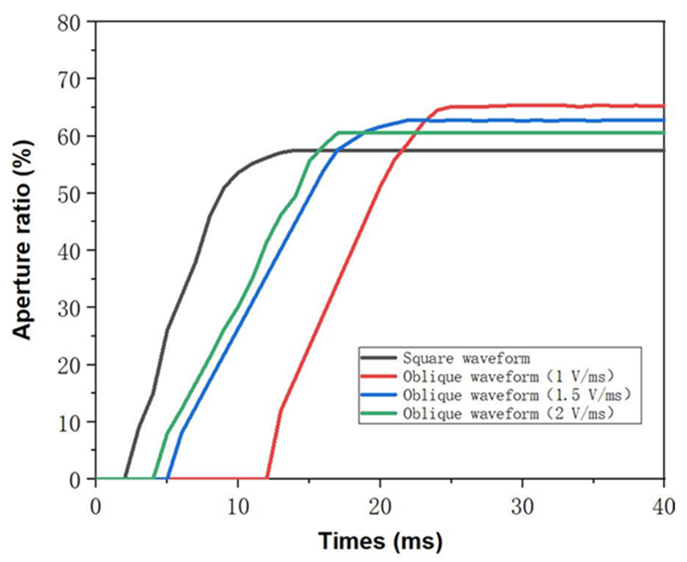
Moreover, the influence of different driving waveforms can be demonstrated by the proposed scheme. Figure 11 shows the aperture ratio curve under different waveforms. From this experiment, we can see that it only takes 12 ms for the EWD pixel unit to be driven by a square waveform from the closed state to the fully open state. However, the maximum aperture ratio of it is the lowest. For the oblique waveform, the average voltage rising speed of 1.5 V/ms and 2.0 V/ms needs 23 and 18 ms from the closed state to the fully open state, respectively. The best contrast performance was obtained under a 1.0 V/ms oblique waveform. However, it is noted that it needs 26 ms to reach the maximum aperture ratio. This display refresh rate is too slow for the multi-gray EWD dynamic display.
The display refresh rate is largely determined by the response time. Therefore, when we set the driving waveform, we needed to consider both the response time and the aperture ratio. By using the proposed detection system, it can be helpful for different EWD devices to find better driving waveforms.
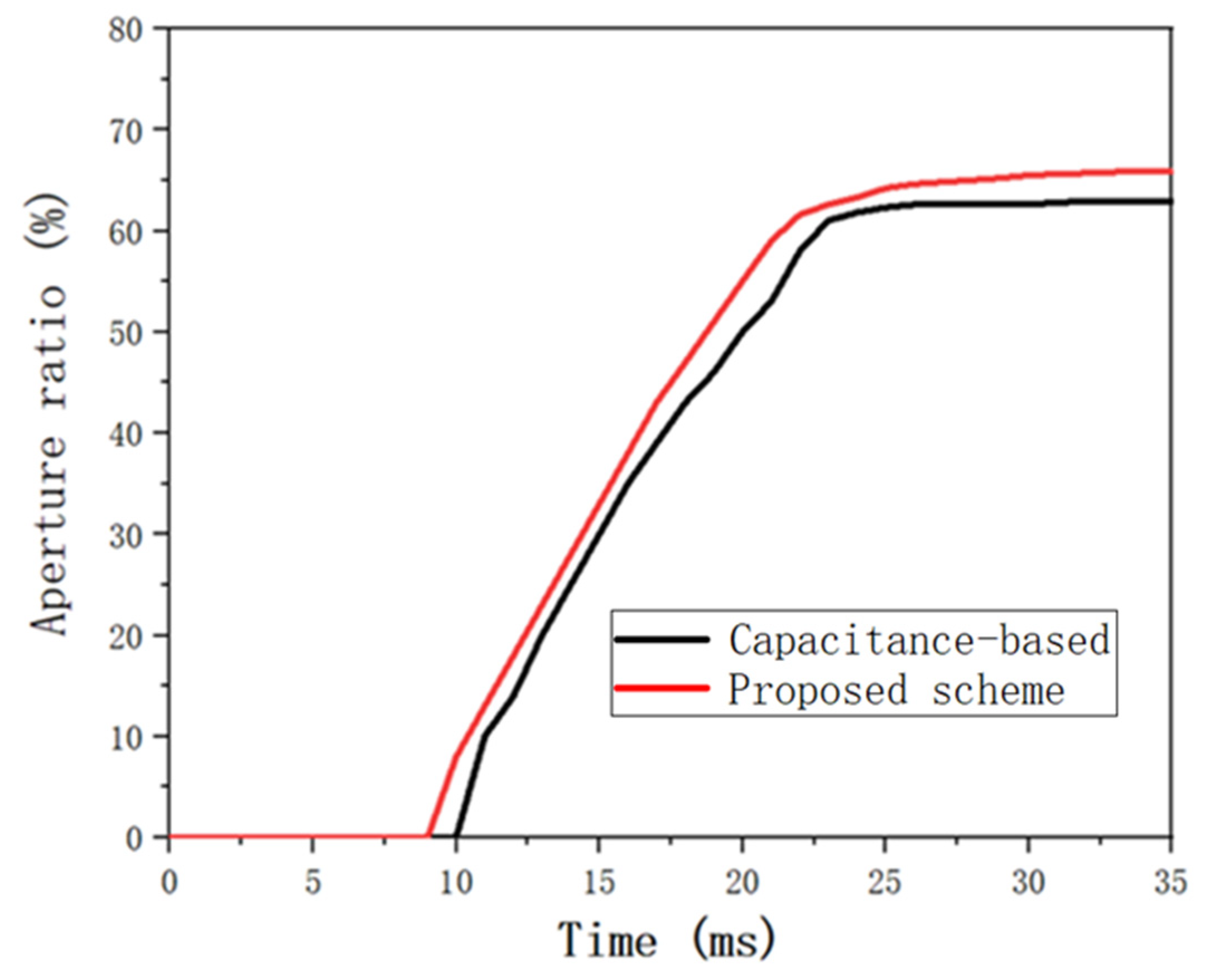
To verify the accuracy of the proposed scheme, we used the capacitance-based EWD detection system developed by our team previously [15] for comparison. The capacitance-based EWD detection method has been proven to be effective and feasible by previous experiments. Both schemes are used to detect the same pixel of an EWD device. The comparison result is shown in Figure 12. It can be seen that the red curve agrees with the black curve in general. The error rate between them is within 6%.

4.3. Oil Motion Defects Detection

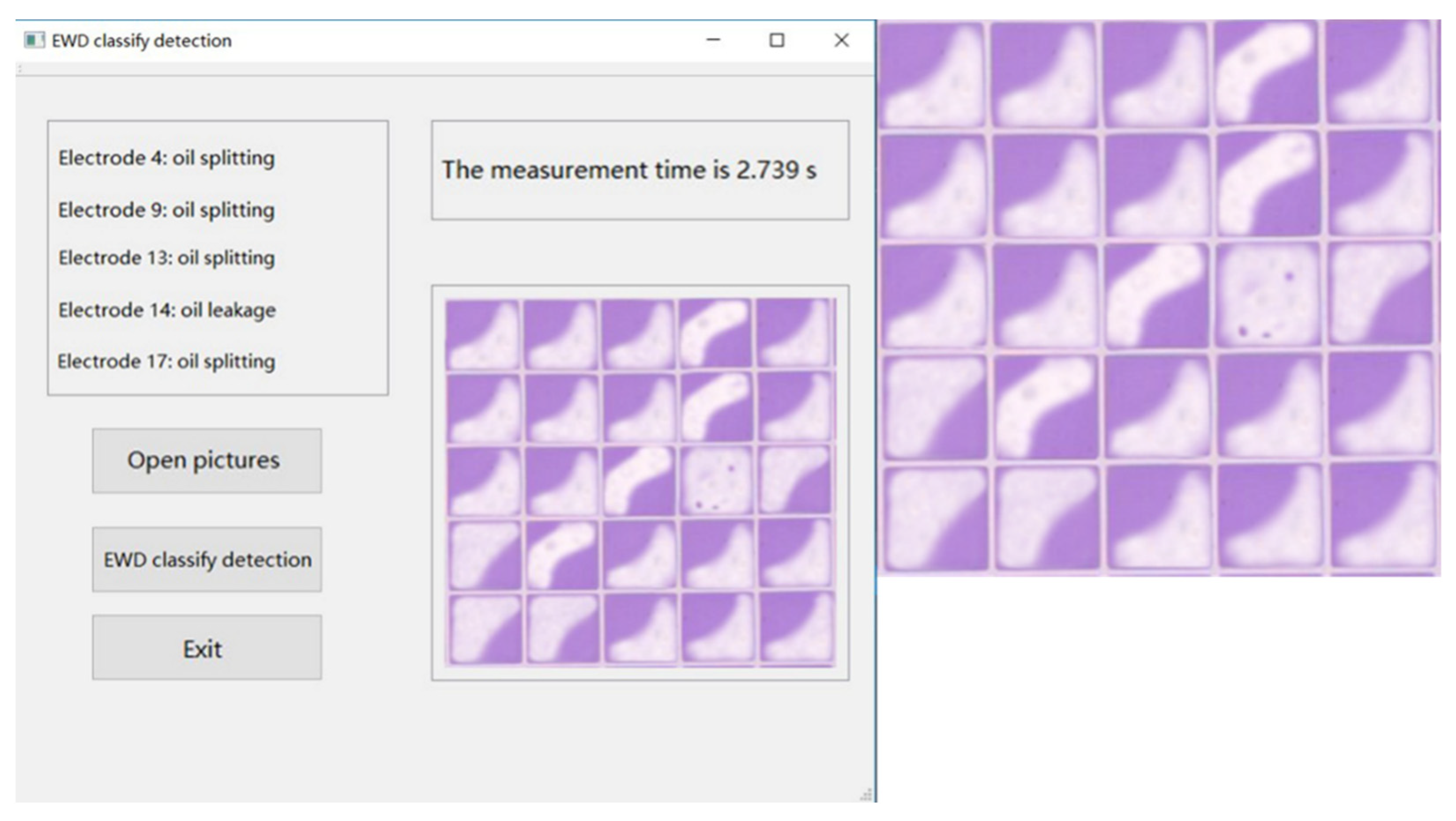
The proposed scheme is used to detect oil motion defects of EWD devices (as shown in Figure 13). Oil motion defects are mostly caused by an improper driving waveform. For EWD, one cycle of the driving waveform includes the rising, display, and reset stages. Different oil motion defects are distributed in different driving stages (e.g., oil non-recovered defect occurs in the reset stage). Hence, the system captures the oil motion from the opening to the maximum aperture and then to the close. By analyzing the morphological characteristics of the oil motion, the proposed scheme can recognize oil leaking, splitting, and non-recovered defects successfully. It should be noted that oil splitting is a repairable defect. To verify the feasibility of the proposed scheme, the square waveform was used for the driving waveform in this experiment.
Table 2 shows the detection results of EWD defects using the proposed scheme. The accuracy of the proposed scheme is over 91% in the case of detecting 25 and 100 pixels. The accuracy of the oil motions defects detection is 84%, even for large-scale EWD devices (324 pixels). For an EWD device with 25 pixels, the measurement time using the proposed method was approximately 5 s. The measurement time increases slightly with the increase in pixels. For 324 pixels, it is approximately 88 s. Compared with the capacitance-based detection scheme, the measurement time of the proposed scheme is greatly shortened. From the experiment result, it can be considered that the proposed scheme can detect the oil motion defects of EWD devices fairly.

4.4. Surface Defects Detection

Due to the immature manufacturing technology, scratch defects (as shown in Figure 14b) are commonly found in EWD devices. Scratch defects are a kind of irreparable defects. It has no fixed shape, and its main image feature is black. Hence, to reduce the interference of oil motion, the proposed scheme detected scratch defects at the reset stage. The scratch detection results are displayed in the GUI (as shown in Figure 14a). In addition, the system records the defective pixel numbers and saves them to the specified directory. Users can query the previous detection results in the history option.
The proposed scheme can also be used to observe the hydrophobic layer state of an EWD device. The hydrophobic layer of an EWD device is easily damaged under long-time high voltage driven. When the hydrophobic layer is damaged, a black spot will appear on the lower substrate surface of the pixel (it can be large or small, depending on the degree of damage), as shown in Figure 15b. Figure 15a shows the variation curve of the hydrophobic layer of an EWD device with 42 pixels detected by the proposed scheme. To validate the feasibility of the scheme, the reset stage and display stage is set to 5 ms and 995 ms, respectively, as shown in Figure 15c. It can be seen that there is a damaged hydrophobic layer when the number of devices driven reaches 1000 in this experiment. The number of pixels with a burned hydrophobic layer increases with the number of devices driven. It is noted that there were nine pixels with burned hydrophobic layers in this EWD device when the number of devices driven reached 3800. It is not an accident that defects are produced in this EWD device even if the display stage is 995 ms (generally, within 300 ms in one cycle). The experimental results show that the reliability and fabrication process of this EWD device needs to be further improved.
The proposed scheme is expected to provide technical support and a platform for improving the reliability of the EWD device and tracing the root cause of defects.

5. Conclusions

A low-cost drive and detection scheme for EWD is proposed and demonstrated in this paper. In this scheme, oil motion performances and defects, including oil leaking, splitting, and non-recovered EWD devices, can be detected and displayed in GUI. Further, surface defects such as the hydrophobic layer burned and scratches can also be captured and analyzed by the proposed scheme. The experimental results show the reliability and feasibility of the proposed scheme in the EWD detection field. The cost of the proposed scheme is low, and it is expected that the scheme presented in this work will provide an efficient and reliable drive and detection platform to other researchers studying in the EWD area. Further, the proposed scheme can be used in EWD-related factories by improving hardware configuration and optimizing detection algorithms in the future.

Author Contributions

Conceptualization, Z.L.; Formal analysis, Y.L.; Funding acquisition, Z.L.; Investigation, B.L., G.Z. and N.C.; Methodology, C.P.; Visualization, S.L.; Writing—original draft, Z.L.; Writing—review and editing, N.C. All authors have read and agreed to the published version of the manuscript.

Funding

This work was financially supported by National Natural Science Foundation of China (nos. 61871475, 61471133), Guangdong Science and Technology Plan (nos. 201905010006, 2017B010126001), the Foundation for High-level Talents in Higher Education of Guangdong Province (nos. 2017GCZX001; 2017KQNCX097), Guangzhou Science and Technology Plan (no. 201904010233), and, in part, by the Guangzhou Rural Science and Technology Specialists Project (no. 20212100058).

Institutional Review Board Statement

The study did not involve humans or animals.

Data Availability Statement

The data used and/or analyzed during the current study are available from the corresponding author on reasonable request.

Conflicts of Interest

The authors declare that there are no conflicts of interest regarding the publication of this paper.

Nomenclature and Abbreviations

EWDElectrowetting display
PSAPressure sensitive adhesive
PCBPrinted circuit board
KNNK-nearest neighbor
MGWFMedian-based Gaussian weighted filter
ROIRegion of interest
GUIGraphical user interface
DACDigital analog conversion
FPGAField programmable gate array

References

  1. Beni, G.; Hackwood, S. Electro-wetting displays. Apply Phys. Lett. 1981, 38, 207–209. [Google Scholar] [CrossRef]
  2. Hayes, R.A.; Feenstra, B.J. Video-speed electronic paper based on electrowetting. Nature 2003, 425, 383–385. [Google Scholar] [CrossRef] [PubMed]
  3. Shufa, L.; Lixia, T.; Shitao, S.; Dong, Y.; Biao, T. An arc multi-electrode pixel structure for improving the response speed of electrowetting displays. Front. Phys. 2022, 10, 706. [Google Scholar]
  4. Fan, M.Y.; Zhou, R.; Jiang, H.W.; Zhou, G.F. Effect of liquid conductivity on optical and electric performances of the electrowetting display system with a thick dielectric layer. Results Phys. 2020, 16, 102904. [Google Scholar] [CrossRef]
  5. Dou, Y.; Chen, L.; Li, H.; Tang, B.; Henzen, A.; Zhou, G. Photolithography Fabricated Spacer Arrays Offering Mechanical Strengthening and Oil Motion Control in Electrowetting Displays. Sensors 2020, 20, 494. [Google Scholar] [CrossRef] [PubMed] [Green Version]
  6. Guisong, Y.; Lei, Z.; Pengfei, B.; Biao, T.; Alex, H.; Guofu, Z. Modeling of Oil/Water Interfacial Dynamics in Three-Dimensional Bistable Electrowetting Display Pixels. ACS Omega 2020, 5, 5326–5333. [Google Scholar]
  7. Zhao, Q.; Ren, W.Q. A finite element method for electrowetting on dielectric. J. Comput. Phys. 2021, 429, 109998. [Google Scholar] [CrossRef]
  8. Lin, S.; Zeng, S.Y.; Qian, M.Y.; Lin, Z.X.; Guo, T.L.; Tang, B. Improvement of display performance of electrowetting displays by optimized waveforms and error diffusion. J. Soc. Inf. Disp. 2019, 6, 619–629. [Google Scholar] [CrossRef]
  9. Zhang, X.M.; Bai, P.F.; Hayes, R.A.; Shui, L.L.; Jin, M.L.; Tang, B.; Zhou, G.F. Novel driving methods for manipulating oil motion in electrofluidic display pixels. J. Disp. Technol. 2016, 12, 200–205. [Google Scholar] [CrossRef]
  10. Wei, L.; Li, W.; Fu, Z.G. Driving Waveform Design for Quick Response Electrowetting Displays Based on Asymmetric Pulse Width Modulation. J. Nanoelectron. Optoelectron. 2020, 15, 1293–1299. [Google Scholar]
  11. He, T.; Jin, M.; Eijkel, J.C.; Zhou, G.; Shui, L.L. Two-phase microfluidics in electrowetting displays and its effect on optical performance. Biomicrofluidics 2016, 10, 011908. [Google Scholar] [CrossRef] [PubMed] [Green Version]
  12. Kim, Y.; Choi, Y.S.; Choi, K.; Kwon, Y.; Bae, J.; Morozov, A.; Lee, H.S. Measurement of the optical characteristics of electrowetting prism array for three-dimensional display. Proc. SPIE—Int. Soc. Opt. Eng. 2013, 8643, 864305. [Google Scholar]
  13. Zhou, M.; Zhao, Q.; Tang, B.; Groenewold, J.; Hayes, R.A.; Zhou, G.F. Simplified dynamical model for optical response of electrofluidic displays. Displays 2017, 49, 26–34. [Google Scholar] [CrossRef]
  14. Deng, Y.; Li, S.; Ye, D.C.; Jiang, H.W.; Tang, B.; Zhou, G.F. Synthesis and a photo-stability study of organic dyes for electro-fluidic display. Micromachines 2020, 11, 81. [Google Scholar] [CrossRef] [PubMed]
  15. Luo, Z.J.; Luo, J.K.; Zhao, W.W.; Cao, Y.; Lin, W.J.; Zhou, G.F. A high-resolution and intelligent dead pixel detection scheme for an electrowetting display screen. Opt. Rev. 2018, 25, 18–26. [Google Scholar] [CrossRef]
  16. Yi, L.; Biao, T.; Guisong, Y.; Yuanyuan, G.; Linwei, L.; Alex, H. Progress in Advanced Properties of Electrowetting Displays. Micromachines 2021, 12, 206. [Google Scholar] [CrossRef] [PubMed]
  17. Li, W.; Wang, L.; Zhang, T.Y.; Lai, S.F.; Liu, L.W.; He, W.Y.; Zhou, G.F.; Yi, Z.C. Driving waveform design with rising gradient and sawtooth wave of electrowetting displays for ultra-low power consumption. Micromachines 2020, 11, 145. [Google Scholar] [CrossRef] [PubMed] [Green Version]
  18. Tang, B.; Groenewold, J.; Zhou, M.; Hayes, R.A.; Zhou, G.F. Interfacial electrofluidics in confined systems. Sci. Rep. 2016, 6, 26593–26599. [Google Scholar] [CrossRef] [PubMed] [Green Version]
  19. Chen, X.; He, T.; Jiang, H.W.; Wei, B.M.; Chen, G.F.; Fang, X.Z.; Jin, M.L.; Hayes, R.A.; Zhou, G.F.; Shui, L.L. Screen-printing fabrication of electrowetting displays based on poly (imide siloxane) and polyimide. Displays 2014, 37, 79–85. [Google Scholar] [CrossRef]
  20. Xu, B.; Guo, Y.; Barman, J.; Erné, B.H.; Deng, Y.; Zhou, G.; Groenewold, J. Impedance analysis of oil conductivity and pixel non-uniformity in electrowetting displays. Results Phys. 2020, 18, 103223–103230. [Google Scholar] [CrossRef]
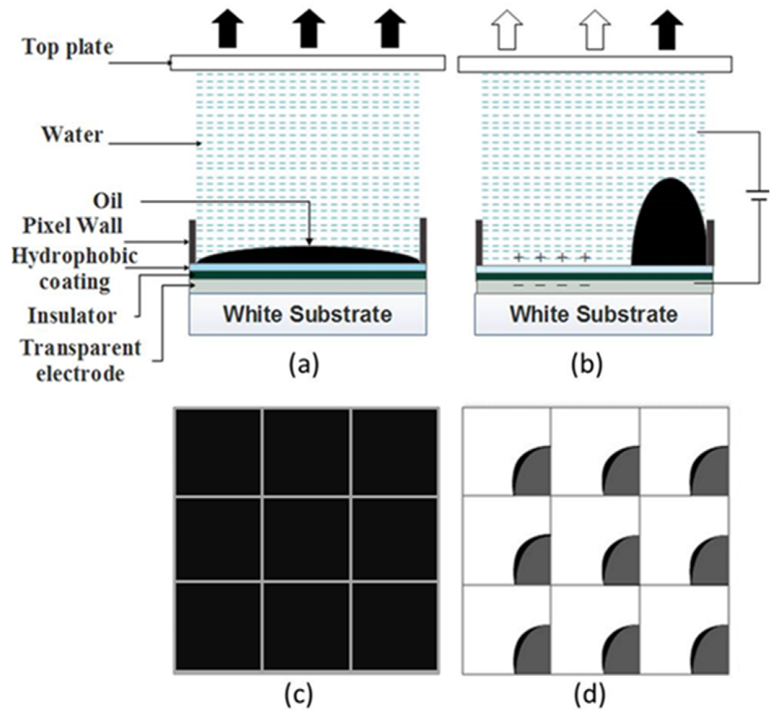
Figure 1. EWD pixel structure and display principle. (a) Pixel is off and black. (b) Pixel is on and white. (c) Upper vision of EWD pixel when it is off (d) Upper vision of EWD pixel when it is on.
Processes 11 00586 g001
Figure 2. (a) Oil-splitting phenomenon in EWD pixels (b) Oil leaking phenomenon in EWD pixels.
Processes 11 00586 g002
Figure 3. The 3D schematic diagram of the proposed scheme.
Processes 11 00586 g003
Figure 4. Block diagram of the detection and feedback mechanism.
Processes 11 00586 g004
Figure 5. Top view of an EWD device.
Processes 11 00586 g005
Figure 6. The complete image processing and analysis solutions for (a) Oil motion performance detection, (b) Surface defects detection.
Processes 11 00586 g006
Figure 7. The system module diagram of proposed driving control system.
Processes 11 00586 g007
Figure 8. The work-flow of the driving control system.
Processes 11 00586 g008
Figure 9. (a) The driving waveform for this experiment. (b) The display result of the square waveform generated separately by proposed scheme and waveform generator on the same EWD device.
Processes 11 00586 g009
Figure 10. (a) The aperture ratio curve of an EWD pixel was detected by the proposed scheme. (b) A screenshot of the EWD detection system.
Processes 11 00586 g010
Figure 11. The aperture ratio curve under different waveforms was detected by the proposed scheme.
Processes 11 00586 g011
Figure 12. The comparison result between the proposed scheme and capacitance-based method.
Processes 11 00586 g012
Figure 13. Oil motion defects detection using the proposed scheme.
Processes 11 00586 g013
Figure 14. (a) EWD scratch defect detection using the proposed scheme. (b) The picture of EWD device captured by camera.
Processes 11 00586 g014
Figure 15. (a) Variation curves of the hydrophobic layer of a EWD device with 42 pixels, (b) Image of burned hydrophobic layer, (c) Driving waveform used in this experiment.
Processes 11 00586 g015
Table 1. The output format of each control unit.
FPGAAD9767 (mA)First Stage Amplification (V)Second Stage Amplification (V)Third Stage Amplification (V)
3FFF+20−1+5+30
0−20+1−5−30
20000000
Table 2. The results of detecting the oil motion defects of different EWD devices.
MethodNumber of PixelsNumber of Oil
Motions Defects
Measurement Time (s)
Artificial observation255NA
10013NA
22529NA
32450NA
Proposed scheme2555
1001223
2252541
3244288
Disclaimer/Publisher’s Note: The statements, opinions and data contained in all publications are solely those of the individual author(s) and contributor(s) and not of MDPI and/or the editor(s). MDPI and/or the editor(s) disclaim responsibility for any injury to people or property resulting from any ideas, methods, instructions or products referred to in the content.