Review

Active Power-Decoupling Methods for Photovoltaic-Connected Applications: An Overview

by
Omar Rodríguez-Benítez
1,
Mario Ponce-Silva
1,*,
Juan Antonio Aqui-Tapia
2,
Óscar Miguel Rodríguez-Benítez
3,
Ricardo Eliú Lozoya-Ponce
4 and
Heriberto Adamas-Pérez
1
1
Tecnológico Nacional de México-CENIDET, Cuernavaca 62490, Mexico
2
John Deere de México, Santa Catarina 66350, Mexico
3
Facultad de Ingeniería, Universidad Nacional Autónoma de México, Mexico City 04510, Mexico
4
Tecnológico Nacional de México–I. T. de Chihuahua, Chihuahua 31310, Mexico
*
Author to whom correspondence should be addressed.
Processes 2023, 11(6), 1808; https://doi.org/10.3390/pr11061808
Submission received: 28 April 2023 / Revised: 30 May 2023 / Accepted: 10 June 2023 / Published: 14 June 2023

Abstract

:
This study compares ripple port, stacked switched capacitor, and capacitive energy storage architectures for active power decoupling, comparing the number of components, performance, energy density, DC-link capacitor reduction, efficiency, and frequency operation to highlight their main benefits and drawbacks for single-phase grid-connected applications. The overview reveals equivalent effective energy density without electrolytic capacitors, as well as enhanced simplicity, performance, and durability, thereby providing stacked switched capacitors as an attractive power-decoupling alternative for multi-stage connected applications, based on the principle that its individual buffer capacitors absorb and deliver energy without tightly constraining their individual terminal voltages, while maintaining a narrow range voltage at the buffer DC port.

1. Introduction

Single-phase inverters must balance AC and DC power for buffering (PBuffer) [1]. Based on the application [2,3,4,5], the input power (PDC) must comply with a small and constant ripple, while the output power (PAC(t)) varies sinusoidally at a twice-line frequency between zero and twice its average value (PAvg(t)) [6]. As Equation (1) shows, a robust element(s) is needed to process the excess energy and optimize energy use.
P B u f f e r ( t ) = P D C P A C ( t ) = P D C cos ( 2 ω g r i d t )
where ωgrid denotes the angular frequency of the line and t the time.
The power pulsation in Equation (1) affects the lifetime of the system, produces large passive components, degrades waveform qualities, reduces the performance, and can deteriorate the maximum power point tracking (MPPT) [7,8]. Consequently, electrolytic capacitors are typically used to store excess energy owing to their high energy density and low cost [9]. However, the use of electrolytic capacitors results in poor energy utilization, short lifetimes, temperature constraints, and an increase in volume [10]. Hence, the development of new decoupling arrangements is important for future grid-connected systems, whose principal characteristics are small size, high energy density, and high reliability [11].
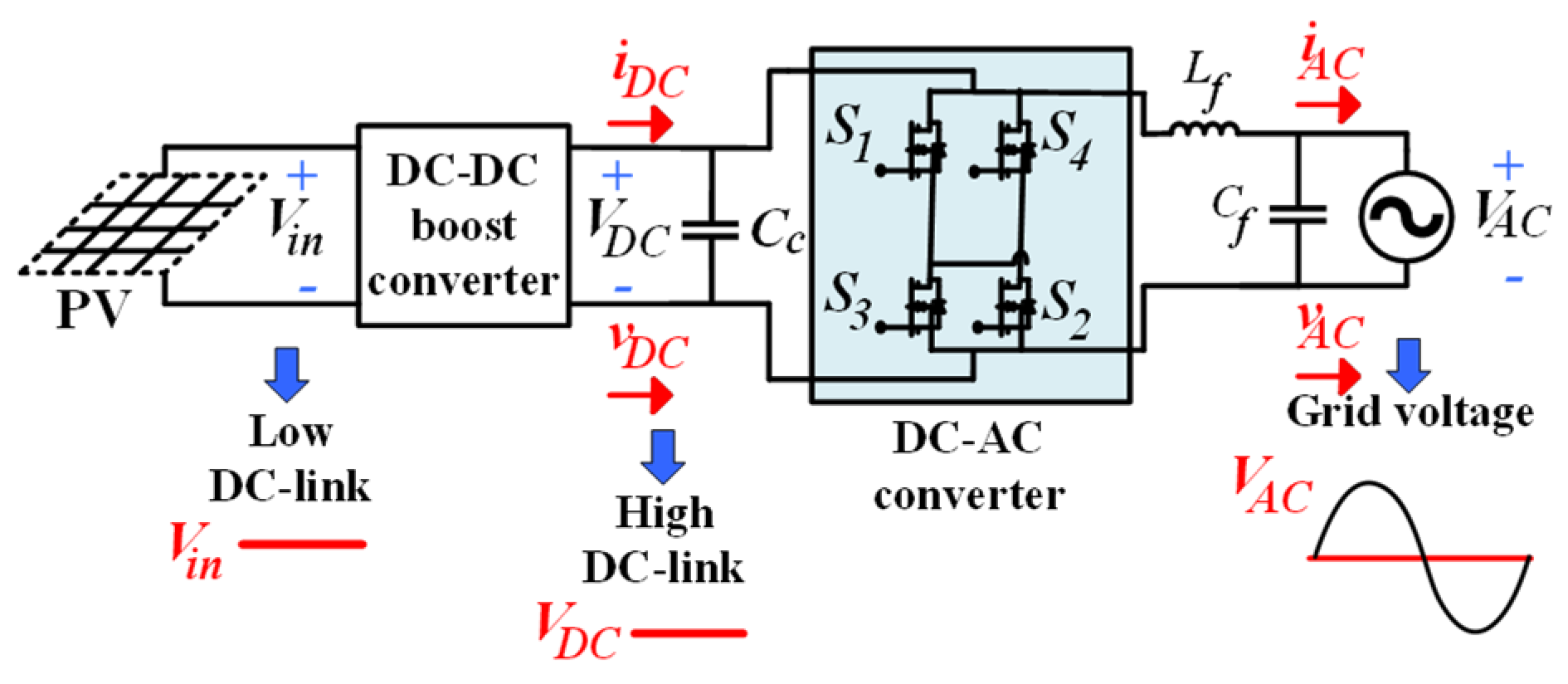
To clarify the earlier physics phenomenon, a conventional grid-connected scheme is shown in Figure 1, where a multi-stage photovoltaic (PV)-connected application is represented [12]. This PV-connected application generally comprises five power stages, in which the use of an electrolytic capacitor (Cc) to decouple the DC and AC sides is expected, but produces high power loss, low reliability, and short lifetime.
In Figure 1, the first stage (Ce) allows low-frequency ripples. In the second stage, according to the inverter specification, the voltage level from the PV is increased (DC-DC). The third and fourth stages represent the inverter (DC-AC) and LC filter, respectively, which must shape the current into a sinusoidal waveform; if the PV array voltage is lower than the grid network voltage, the PV array voltage must be boosted with an additional element. Finally, the fifth stage filtered the sinusoidal signal using a second-order LC filter.
According to the component characteristics in the third stage, many alternative solutions have been proposed to avoid the use of a bulky and low-reliability device [13,14,15,16,17]. Some of these solutions have been classified into two principal groups [18,19,20,21,22,23,24,25,26]: passive and active power-decoupling methods (PPD and APD, respectively). The former methods commonly apply an LC filter or bulky passive components (inductor or capacitor), while the latter provides many attractive features, such as a relatively small size and high reliability, because it stores the ripple power in another component by adding an extra switching circuit.
From this classification, one interesting PPD method for eliminating the use of electrolytic capacitors is the current source converter (CSC) [27,28]. The CSC has as principal advantages a continuous input current and high voltage gain, making it an interesting option for a single-phase connected application. However, CSCs present some drawbacks, such as the need for a large and bulky inductor, low efficiency, complex control, and poor power density.
Similar to the CSC, the passive LC branch for bypassing the power decoupling [29] represents another PPD method, which generates an AC current that compensates for the twice-line frequency ripple. However, the resonant circuit is sensitive to voltage distortion in the grid network, and the voltage across the capacitor of the LC circuit can be significantly higher than the maximum DC-link voltage. It also presents high oscillations, adds more weight and size to the system, and is still not cost-effective owing to the low-frequency LC circuit.
Different to the PPD method, the APD applies an extra switching circuit to store the energy [30,31]. One alternative to this method is the use of bidirectional DC-DC converters to effectively utilize film capacitors while maintaining the desired narrow-range bus voltage [32]. However, owing to the power losses in the DC-DC converter, these solutions present low buffering efficiency if high power density needs to be maintained.
Another APD method involves injecting a second or fourth harmonic into the circulating current to balance the grid power at higher frequencies [33], aiming to apply small capacitors because a large voltage ripple across the decoupling component can be applied. However, these methods are not entirely convenient for grid-network-connected PV applications because they are preferable for motor drives, wind turbines, and LED applications at low frequencies and modulation indices [34,35]. In addition, these techniques are generally used by adding an extra DC-DC bidirectional converter; the smaller the capacitor, the greater the stress on power semiconductor devices, which results in increased losses when a high power density is to be maintained, and consequently, lower efficiency is achieved.
Other APD solutions have been proposed based on boost-buck and buck-boost inverters [36,37]. These works are generally aimed at achieving low AC distortion, small volume, and high efficiency. However, they do not entirely represent the stability of current injection into the utility grid network.
The use of current control in parallel with a decoupling capacitor is another APD solution [38]. This active technique controls and reduces the amount of current drawn from the capacitor, thereby effectively reducing the need for energy damping [39,40,41,42,43]. However, the voltage across the switches is very high because the switches can be exposed to voltages as high as the DC link, increasing the switching losses of power semiconductor devices.
Similar to the previously mentioned topologies, the flyback-type inverter is another topology to permit small-volume, lightweight, and stable AC current injection into the utility grid network [44,45]. This type of solution almost removes low-frequency power pulsation, with the aim of using small capacitors. However, their efficiency is significantly affected by high power losses in power semiconductor devices. In addition, its use is suggested in low-power applications.
In contrast to earlier methods, alternative active filter configurations were introduced in the form of stacked switched capacitors (SSCs) [46,47], voltage capacitor active power decoupling (VCAPD) [48], and ripple-port module-integrated inverters (RP-MIIs) [49]. The first presents a bipolar or unipolar architecture to replace the electrolytic capacitor, the second one stores the power ripple on the capacitor, while the last applies a third port on the DC link for ripple cancellation purposes, which is added to the converter, and handles approximately one-third of the total energy in the system. These techniques maintain comparable effective energy densities, require a very small DC-link capacitance, and can be applied in any isolated boosting DC-DC converter.
In a brief review, one of the principal drawbacks of the PPD method is the need to apply almost infinite values of passive components to become approximately constant voltage and current at the DC-link, causing a large volume and weight in the entire system. In contrast, the APD solution permits an increase of approximately 50% in the power density, thereby providing these methods as attractive solutions to decouple the twice-line frequency ripple.
In this regard, the main contribution of this study is to provide a comprehensive review of APD methods, mainly referring to the solutions presented for SSC, RP-MII, and VCAPD in single-phase, multi-stage, isolated PV-connected applications, by comparing the number of components, performance, energy density, reduction of decoupling components, efficiency, and frequency operation. The present study differs from different works introduced earlier, such as the one presented in [50], where its main contribution is focused on control strategies in APD, or [51], where it focuses on the evolution of control algorithms in power system support functions, such as voltage and frequency regulation, while also offering an overview of power system support functions derived from renewable distributed energy resources (DERs). In addition, this study differs from some reported techniques focused on the AC side, such as parallel power factor corrections (PFCs), DC-bus conditioners, AC-side active filters, and two-stage cascaded PFC, because all these methods are applied to solve the second-order harmonic current issue presented in single-phase pulse-width modulation rectifiers [52].
The remainder of this paper is organized as follows. Section 2 describes the operational principles of SSC, RP-MII, and VCAPD methods. Section 3 presents a general overview of the selected APD methods by comparing the number of components, performance, energy density, reduction of the decoupling element, efficiency, and frequency of operation. Section 4 provides a discussion and comparison. Finally, Section 5 concludes the paper.

2. The Principal Operation of the SSC, RP-MII, and VCAPD Methods

2.1. SSC Architectures

The use of SSC architectures, which reconfigure capacitors between parallel and series combinations to decouple power energy, results in an interesting alternative for improving energy utilization [53]. This method adds a switching circuit that includes a block of capacitors and switches to eliminate the use of electrolytic capacitors.
In this regard, the energy buffer, by applying SSC configurations, works on the principle that each capacitor absorbs and delivers energy, maintaining a narrow range of voltage at the buffer port, allowing maximum utilization of the energy storage capability [54]. Another approach to increasing the energy density is to optimize the capacitance ratio of the capacitors used in the energy buffer [55,56].
There are two blocks within these architectures: the backbone and supporting capacitors. The first buffers most of the total energy utilized, and the second provides voltage support, maintaining the total bus voltage in the desired range (Figure 2). In addition, the backbone capacitors have components that reflect the performance of the DC-link capacitor as if it was just one component, while the supporting capacitors included components that helped to maintain the voltage level in the principal block, allowing the preservation of the necessary energy to the load.
In Figure 2, the decoupling circuit is presented with two systems of general architecture: unipolar (Figure 3a) and bipolar (Figure 3b) [57,58]. The former is suggested in low-power applications and is composed of series-connected support, backbone blocks of switches (S1, S2, and Sm), and capacitors (C1, C2, and Cm). The latter provides a support block comprising an H-bridge (SH1, SH2, and SH3, SH4), switches (S2, S2m), and capacitors (C2b, C2mb) in combination with backbone capacitors (C1b, Cmb) and switches (S1, Sm). This architecture is suggested for high-power applications and has a principal characteristic that it can be applied to as many capacitors and switches as required.
The unipolar scheme shown in Figure 3a, consists of one backbone capacitor (C1), m supporting capacitors (C2, and Cm), and m + 1 supporting switches (S1, S2, and Sm). This architecture is called the 1-m enhanced unipolar design, in which conventionally all capacitors present the same value of capacitance, but different voltage ratings. For this architecture, once the buffer starts, S1 is turned on, while the rest of the switches are turned off, charging the backbone capacitor C1 until a specific bus voltage. When this voltage is reached, S1 is turned-off and S2 turned on, allowing the charge of the supporting capacitor C2; this process continues until the rest of the supporting capacitors are charged and discharged during a complete period (the switches are turned on and off in reverse order during the discharging cycle).
According to the literature, for a 1-m unipolar architecture, the energy buffering ratio ( Γ b ) can be defined as
Γ b = C 1 ( ( 1 + R v 2 ) ( 1 m R v 2 ) ) + ( m R v ) 2 C 1 ( 1 + R v ) 2 + C 2 ( 1 + 2 2 + 3 2 + + m 2 ) R v 2
where Rv is the bus voltage ripple ratio, defined as
R v = V max V min 2 V n o m
In Equation (3), the maximum, minimum, and nominal voltage values are represented by Vmax, Vmin, and Vnom.
The architecture in Figure 3b, presents a scheme comprising n backbone capacitors (C1b, Cmb), m supporting capacitors (C2b, C2mb), and switches (n + m + 4 switches). This architecture is called an n-m enhanced bipolar design, in which all capacitors have equal capacitance, but different voltage ratings. This architecture permits an increase in the energy buffering ratio because it provides an energy buffering capability of 71.1% of the total peak energy storage [59]. For this architecture, C1b can be increased to Cmb backbone capacitors as needed, as well as the supporting capacitors from C2b to C2mb.
An interesting point to note is the fact that for the bipolar architecture, the values of the backbone and supporting capacitors are the same, but with different voltage ratings; however, the supporting capacitors are put into an h-bridge to enable bi-directional charging.
According to the efficient charging and discharging process of the capacitors shown in Figure 3, the energy density can be increased. Further, the voltage ratings in all capacitors can be optimized. This point is critical because the voltage rating depends exclusively on the Vnom of the bus voltage (Vbus).
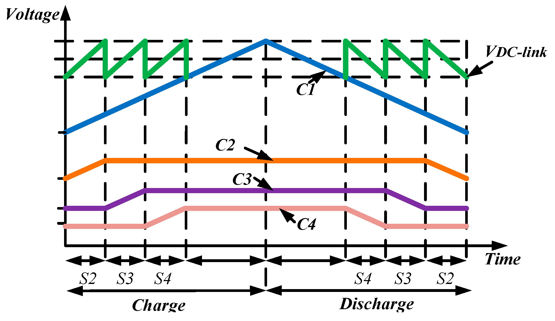
On the other hand, the capacitors for both versions of architecture must be pre-charged through a specific sequence, so that at the beginning of the discharge cycle, all the capacitors are charged to their maximum level, the first to discharge being the backbone capacitor. Once the voltage on the DC-link (VDC-link) reaches its minimum allowed value, the supporting capacitors are charged/discharged one by one in each transition, so that the capacitors that were used in the previous cycle can be loaded independently. Figure 4 shows an example of unipolar architecture according to a charged and discharged cycle, where the supporting capacitors (C2, C3, and C4) are added one by one to the backbone capacitor (C1) to obtain the desired behavior for energy damping.
A key point to achieve high efficiency in SSC architecture is to define correctly the commutations shown in Figure 4 (for S2, S3, and S4). The efficiency of the SSC system across a full operating range can be especially high because the grid network only operates at very low switching frequencies, reducing losses.

2.2. Capacitive Energy Storage for Ripple Power Compensation

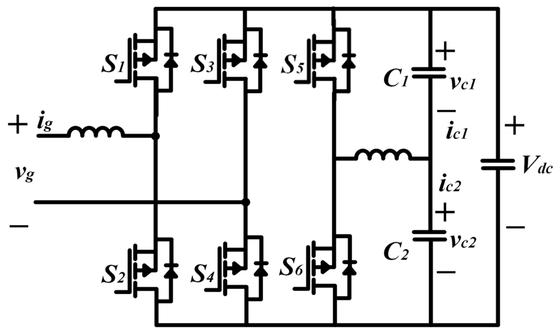
As an alternative to SSC architecture, power decoupling based on capacitive energy storage consists of a storage capacitor (Cdc), a full H-bridge (T1, T2, T3, and T4), and an additional third leg (T5, and T6), which is composed of an energy storage variable capacitor (Ccx) and a smoothing inductor (Lc), as shown in Figure 3a of the study published in [61], where the inductor Lc is used to absorb the high switching frequency ripple, and La, Lb, which are utilized to filter the input signal.
The reference voltage for the capacitor Ccx is a sinusoidal waveform operating at a similar frequency to the AC source (Vs). As the operating frequency is low, this method can achieve a good power decoupling performance at low switching frequencies. The processed energy Ccx is controlled by the additional phase leg to absorb the 2 ω ripple. Thus, Ccx can be fully charged to Vs and discharged to its voltage −Vs; as a result, this approach only requires a minimum DC capacitor and a minimum AC capacitor to implement its function.
The VCAPD control system consists of an inner loop control and an outer loop proportional resonant control.
The control system first suppresses the high resonance peak, and then it uses a proportional resonant controller on the outer layer to achieve steady-state precision. The capacitor voltage reference is modified through the closed-loop control. The main idea is to compensate the ripple power based on the control of the capacitor voltage or capacitor current.
From Figure 3a in [61], the reference voltage for the capacitor (Vcx) is a sinusoidal wave with the same frequency as the Vs. On the other hand, due to the use of a capacitor as an energy storage component, the electrical efficiency is higher than using inductors. Moreover, the current stresses of the rectifier legs (ia, ib, and ic) do not increase.
The first step of parameter design for the VCAPD method is to choose an appropriate LC resonant frequency. Apart from setting the upper limit of the system bandwidth and directly determining the cancelation of two coefficients, it has an impact on many other variables. It is important to note that the total capacitance can be reduced by almost five times.
To verify the performance of the VCAPD method, there are some reported works. For example, Figure 9 of the study published in [62] shows the simulation results of the PWM rectifier, where va, vb, and vc are the phase voltages; vcac is the voltage in the storage capacitor (cac); Vs is the input voltage; is is the input current; icac is the current in cac; and vdc is the voltage in the output capacitor.
On the other hand, the literature also shows that some of the principal advantages of applying the VCAPD method are high efficiency compared to inductance energy storage, a low requirement for switching frequency/control bandwidth, full utilization of the energy storage capability, and no excessive current stresses for the power devices [63]. Therefore, this method can increase the life expectancy of a power supply.
Compared with the LC resonance filters tuned at twice the grid frequency, the passive components in the VCAPD circuit are also greatly reduced. Furthermore, the voltage rating of the capacitor is lower than in passive LC filters. To enhance the power decoupling performance, a closed-loop modification of the capacitor voltage reference based on the residual ripple voltage is carried out.

2.3. RP-MII

To demonstrate the analysis of the RP-MII, a conventional single-phase grid-connected structure is shown in Figure 5 [64].
In Figure 5, Vin is the input voltage; Cc is the decoupling capacitor; iDC and vDC are the current and voltage, respectively, across Cc, and Lf, Cf, which are utilized as filter steps.
From Figure 5, the current (iAC) and voltage (VAC) that fluctuate in the grid network can be determined as
V A C t = V D C c o s ω t
i A C t = I D C c o s ω t α
where VDC and IDC are the DC-link voltage and current, respectively; ω is the angular frequency (2πfgrid); fgrid is the grid frequency (60 Hz); and α is the angle between the AC voltage and the current.
Since the AC-side power fluctuation is the product of VAC and iAC, the AC power (PAC) can be calculated as
P A C = V A C i A C
From the previous equation, by applying the trigonometric identity in Equation (7), PAC is defined as shown in Equation (8).
cos 2 ( ω t ) = 1 + cos ( 2 ω t ) 2
P A C = 1 2 V D C I D C cos ( 2 ω t + α ) ( 1 ) + V D C I D C cos ( α ) ( 2 )
From Equation (8), term 1 represents the power ripple (Prip), which causes a voltage variation in the DC-link that is reflected at the PV terminals (in this example), causing an efficiency reduction. When PAC is greater than the power in the DC-link (PDC), the difference in Prip is absorbed by the power decoupling component. Alternatively, when PAC is less than PDC, the decoupling component must deliver the stored power to compensate PAC and ensure energy conservation.
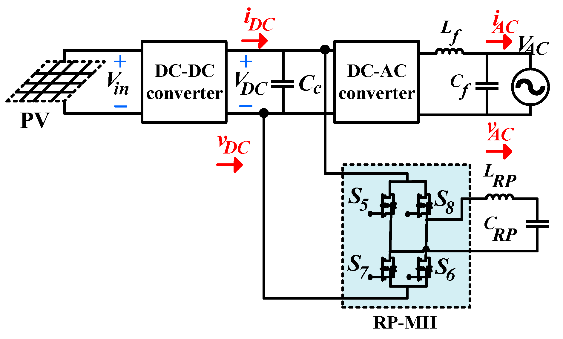
Term 1 from Equation (6) is crucial to demonstrate the power decoupling strategy by applying an RP-MII scheme. This configuration is shown in Figure 6 [64].
The scheme in Figure 6 presents a single-phase connected system that applies a RP-MII as a power decoupling method. This system is made up of a magnetically isolated DC–DC converter (to adjust the voltage level provided by the PV), an inverter, and a ripple port that is responsible for mitigating power fluctuation.
Power decoupling through an RP-MII consists of adding a circuit comprising a full H-bridge inverter (S5, S6, and S7, S8) and a second-order arrangement made up of LRP and CRP. From this arrangement, LRP is used to prevent any sudden voltage changes, while CRP is used to serve as a support component for Cc, avoiding a high-voltage ripple on the DC-link.
Similar to the scheme shown above, it is expected that the DC port provides a nominal power value that, for practical purposes, is as close as possible to the average value of the power demanded by the load. However, as this condition never occurs, the power managed by the ripple port is essential for energy conservation.
Therefore, the main function of the RP-MII is to process the PDC, which means that the total power in the RP-MII (PRP) can be approximated as the sum of the average power in LRP (PLRP) and CRP (PCRP), as follows.
P R P = P L R P ( t ) + P C R P ( t )
From Equation (9), since the current through LRP and CRP is the same, PRP can be expressed as
P R P ( t ) = C R P V C R P ω sin ( ω t + α ) V C R P ( t ) C R P V C R P ω sin ( ω t + α ) ( V C R P ( t ) )
where VCRP is the voltage across CRP, and by applying the trigonometric identity in Equation (11), it is possible to reduce Equation (10), as shown in Equation (12).
( sin ( 2 α ) = 2 sin ( α ) cos ( α ) )
P R P ( t ) = V C R P 2 C R P ω ( 1 ω 2 L R P C R P ) 2 sin ( 2 ( ω t + α ) )
From Equation (12), it is possible to determine CRP. This value is shown in Equation (13).
C C R P ( t ) = V C R P 2 8 P D C ω L R P 4 ω 4 L R P 2 V C R P 2 + 1 2 ω 2 L R p
The scheme shown in Figure 6, is based on adding a port that processes only the minimum value of energy required. Therefore, due to the benefits offered by this topology, it is necessary to carry out an analysis that obtains the performance values that define its operation, advantages, and drawbacks. Therefore, Section 3 presents a comprehensive review focused on SSC architecture, the VCAPD method, and RP-MII as power decoupling strategies.

3. Overview

3.1. SSC as an APD Method

SSC architecture can achieve greater energy efficiency and a substantial reduction in the decoupling capacitor thanks to the effective use of stored energy. In this meaning, the energy buffering ratio (EBR) represents the total energy extracted from the buffer, while a higher EBR lowers the energy storage requirement, allowing a considerable reduction in passive volume. This means that the EBR is a key parameter for the verification of the optimal performance of the energy buffer.
A bipolar SSC architecture that analyzes part of these characteristics is [65], and it is essentially introduced to solve low efficiency in high power (2 kW) as a result of the control strategy applied. Its principal contribution is a variable-frequency, constant, peak current control strategy, which permits a performance of 90% of efficiency by applying power semiconductor devices based on silicon carbide (SiC). This scheme is shown in Figure 3 of the study published in [65].
The scheme in Figure 3 from [65] presents a bipolar energy buffer architecture comprising a supporting block (C21, C22, C23, C2m with S21, S22, S23, S2m as switches, respectively, and a full bridge SH1, SH2, SH3, and SH4), a backbone block (C11, C12, C1n with S11, S12, S1n as switches, respectively) that pre-charges all the capacitors at the beginning of the switching period, a DC–AC inverter, and a filter stage.
This topology performs the SSC arrangement across the DC input bus, and one of the principal characteristics is the performance provided by its control strategy. This control permits the commute of part of the DC–AC converter at a high frequency to shape an output current, while the rest of the converter commutes at line frequency. This characteristic allows an optimal choice of inductor peak current (at the filter stage), improving the efficiency over varying average power levels, simplifying the EMI filter design, and reducing the switching losses.
Alternatively, according to the results provided by the authors, addressing the energy density, based on the nominal voltage under the ceramic capacitors implemented, permits the observation of the real minimization of the total volume under the selected scheme.
Similar to the previous architecture, work [66] presents a topology where a large portion of the energy used is extracted by the arrangement in the backbone capacitors. The high energy density reduces the passive volume requirement according to the ripple voltage, so the capacitors used in the energy buffer have a similar capacitance with a different voltage rating. A pre-charge circuit ensures that the initial voltage is applied to the buffer capacitors. The SSC architecture is presented in Figure 7.
In contrast to the earlier works that utilized backbone and supporting capacitors with equal capacitance values, work [67] is a SSC architecture whose principal contribution is an optimization methodology that achieves a substantial increase in the effective energy density of the SSC energy buffer. This methodology optimizes the capacitance ratio of the capacitors used, in which the ripple ratio and the number of capacitors affect directly the increment of the energy density. With this capacitance, it is possible for the optimization to increase the effective energy density by 100% in a 1–10 enhanced unipolar architecture (with a 10% DC-bus voltage ripple) in comparison to when the energy buffer is designed with equal capacitance values. This optimization permits a higher effective energy density and lower passive volume. The architecture based on SSC is an interesting APD method to implement for a twice-line power variation.
Another important point mentioned in the literature is that the bipolar scheme offers higher energy buffering at lower voltage ripple ratios than the unipolar scheme. This is not completely true, because according to [67], a higher ripple ratio allows a superior energy buffer performance; this means that the energy stored is a larger fraction of the energy buffer.
The optimal capacitance ratios in an SSC scheme permit a substantial improvement in the energy buffering ratio. This, in combination with the optimal choice of the capacitor, helps to enhance the energy buffering ratio. For example, from [67], for a 1–2 unipolar scheme designed for a 5% voltage ripple ratio, it is possible to have a reduction in the passive volume of 17%. Moreover, for a 1–10 unipolar architecture, it is possible to achieve a 100% increase in the energy buffering ratio. This increment presents a significant opportunity to increase the energy density of similar schemes, as shown in Figure 1.
Similar structures using the SSC method have been presented in the literature. Table 1 lists some principal reported works, where the electrical efficiency, power rating, and reduction of capacitance were considered as key comparison parameters. The maximum reduction and maximum efficiency were obtained with a 7.5 times reduction and 98.5% efficiency.
Finally, as a summary, the principal characteristics of the SSC method are listed in Table 2.
As described above, unipolar and bipolar SSC energy buffer architectures have advantages that present them as an interesting APD alternative. Furthermore, both architectures present enhanced variants that permit them to increase the energy density and reduce volume. This improved performance is realized in the unipolar case by adding an extra switch, in the bipolar case by modifying its control stage, or in both cases by optimizing the capacitance ratio of the capacitors used.

3.2. VCAPD as an APD Method

Similar to the SSC architectures, the VCAPD method focuses on reducing the DC-link capacitor. This means that some topologies store energy in one inductor or capacitor. A focused work on a VCAPD method is [71]. The scheme is shown in Figure 8 and comprises a full-bridge inverter (S1, S2, S3, and S4) and a half-bridge inverter (S5, and S6), which are considered as the load arrangement made by Cd and Lcx. In this scheme, the power ripple is transferred to Cd, and the voltage on the Cd capacitor is controlled as a DC component superimposed with a second-order harmonic. However, rich harmonic content in the reference signal poses a challenge for controller design, and the problem gets worse for high-power applications, where the switching frequency is limited. So, the energy storage is greater than the energy used, ideally.
The PWM rectifier system with two capacitors (C1 and C2) as energy storage elements is shown in Figure 9. The power on C1 and C2 is equal to the ripple power; by controlling this power, the total capacitance required is less by using a single capacitor. Moreover, the capacitors C1 and C2 are used as DC filter capacitors. One disadvantage is the required DC voltage, because it is the sum of the voltage in C1 and C2. Therefore, the energy of C1 and C2 are not completely used for the compensation of the ripple power.
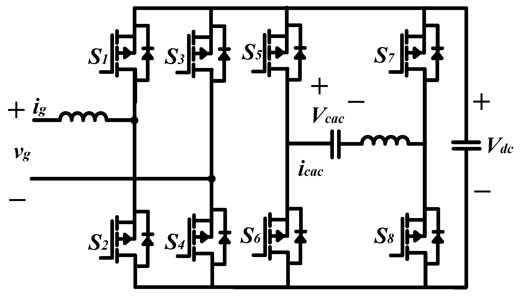
Another alternative to this idea is to replace the LC circuit by applying a full-bridge inverter in parallel to the DC-link capacitor (Figure 10). The Lac-Cac circuit is used as a load in the inverter, so sinusoidal waveforms are obtained in Cac. Based on the processed energy in Cac, the DC capacitance is reduced. One drawback is the use of two extra switches to the half-bridge proposal.
Another approach based on VCAPD with minimum DC capacitance was introduced in [72]. Adding a phase leg in parallel to the full-bridge inverter and considering the Lc series circuit, the component can be absorbed, and the DC capacitance is reduced.
The method presented is shown in Figure 3 of the study published in [72]. Basically, by controlling the angle between the input voltage vs. and the input current is (which has the same value as ia), the inverter acts as a pure capacitor. Meanwhile, by controlling the amplitude of is, the inverter can achieve continuous variable capacitance. Therefore, the inverter can be considered a variable capacitor.
A constant voltage across the DC capacitor Cdc is needed to operate the H-bridge inverter as a variable capacitor. The reference voltage for Cac is a sinusoidal wave in the same frequency as the AC input voltage. Since the capacitor is always totally charged and discharged, full utilization of its energy storage capability is also attained. Furthermore, it was shown by the analysis that the current stresses of the two rectifier legs were not increased.
The three-phase legs can be modeled as a controlled voltage source, as shown in Figure 4 of the study published in [72]. To compensate for the grid side ripple power, the power reference of Cac (PCac) should be controlled to be equal to the ripple power (Pripple); so, the energy of Cac (Ecac) should be
E c a c = 1 2 C a c v C a c 2 = P C a c = P r i p p l e = v s i s
As shown in Equation (14), the ripple power is equal to Ps and can be calculated based on vs. and is. The capacitor voltage and current reference are accurate and simple to calculate directly, based on the power reference. The grid power reference has two parts: the DC component and the ripple AC component. Thus, by using a high-pass filter, the ripple power is obtained.
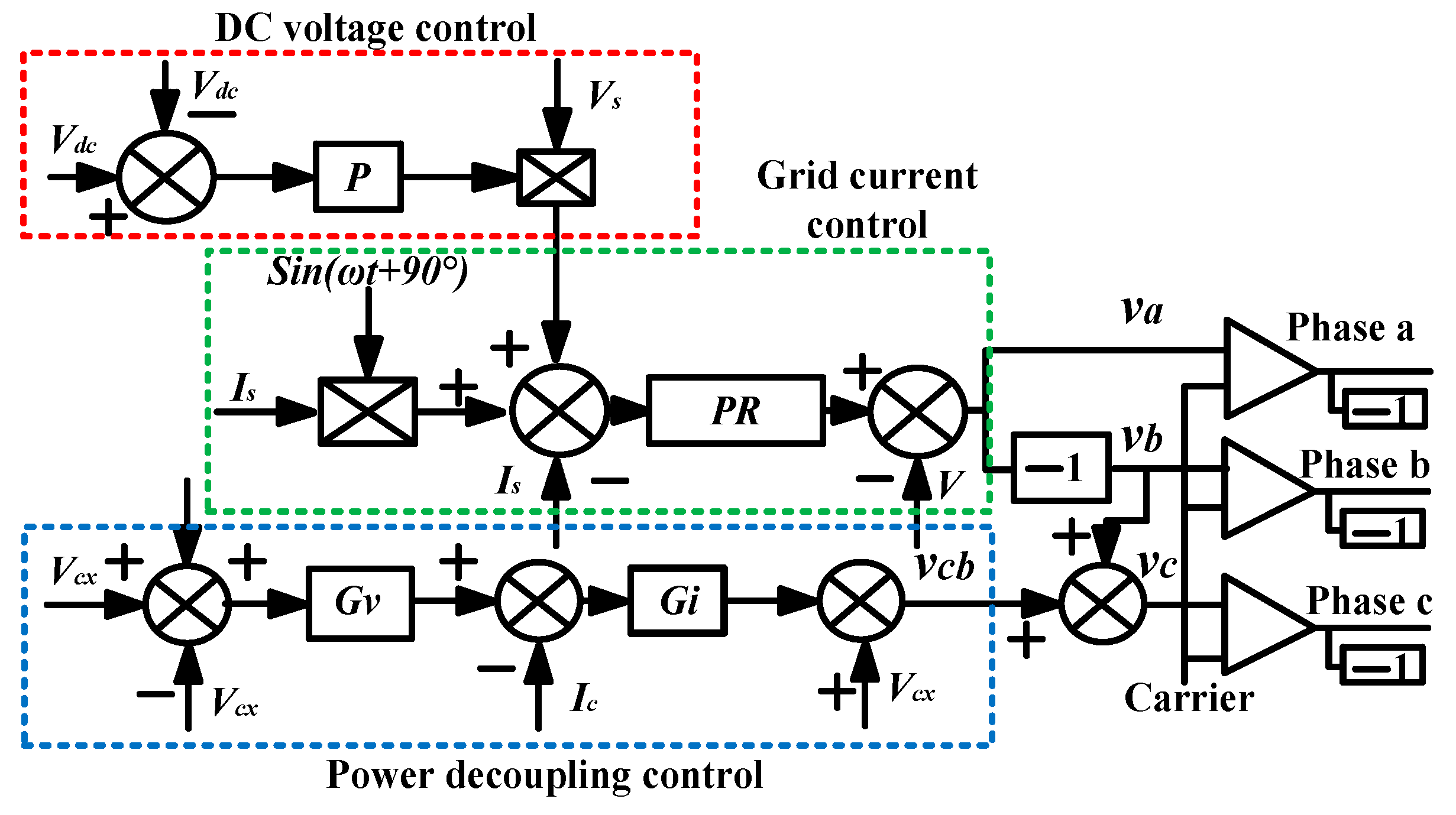
Figure 11 shows the overall control diagram of the active power decoupling. It consists of three controllers: the DC voltage controller, which maintains the DC-link voltage Vdc; the grid current controller, which takes charge of reactive power control; and the power decoupling controller, which controls the AC capacitor voltage Vcs and current Ic.
Experimental results show the capacitance reduction is nearly 13 times that of the conventional H-bridge inverter. This clearly shows that the advantages of this proposal are promising; however, the power density is not mentioned, and the control strategy is complicated. Furthermore, there are some problems related to the PR controller: its gain is much reduced at other frequencies, it is not adequate to eliminate harmonic influence caused by grid voltage, and the tuning process is difficult to achieve.
Another proposal is presented in [73], where a new current source converter topology for PV applications is detailed. The main advantages of this proposal are that the low ripple power was eliminated, the power density was increased because of the non-use of electrolytic capacitors, and the maximum power point tracking was improved.
The circuit proposed is shown in Figure 2 of the study published in [73]. The bidirectional switches are implemented by a series of an arrangement made by a diode and an IGBT. An inductor Ldc is placed in series with the PV. In a typical single-phase inverter, Ldc has to be a significantly large size to maintain the double-frequency ripple current, which results from the pulsating instantaneous power flow, at a sufficiently low level for proper operation of the converter. However, the DC link inductor in this topology is sized according to the switching frequency ripple components. Therefore, the size of Ldc is smaller than a conventional single-phase inverter.
In the case of the AC side of the converter, phase-legs a and c of the bridge are connected to the grid voltage vg through an Lf-Cf filter. The phase-leg b of the converter is connected to the grid through Cb. The voltage across the Cb depends only on the current flowing through phase-leg b. With proper control of the current ib, it is possible to achieve a constant instantaneous power flow across the bridge. Thus, the low-power ripple is reduced.
Similar structures under the VCAPD method have been presented in the literature. Table 3 lists some of these principal reported works, where the electrical efficiency, power rating, and reduction of capacitance were considered as key comparison parameters. The maximum reduction and maximum efficiency were obtained in [74], with a 12.6 times reduction and 93.7% efficiency.
Finally, as a summary, some of the principal characteristics of the VCAPD method are listed in Table 4.
As described above, the VCAPD method focuses attention on the reduction of the DC-link capacitor by varying the voltage across a passive component. In the case of the inductor, its low power density and high-power losses result in a poor strategy. However, as the literature shows, energy optimization by applying a capacitor is more efficient, and with this strategy, it is possible to reduce the DC-link capacitor up to ≈13 times from its nominal value.

3.3. RP-MII as an APD Method

Similar to the SSC and VCAPD methods, RP-MII as a power decoupling structure focuses attention on the reduction of the decoupling DC-link capacitor. According to the RP-MII definition, there are two operation approaches. One is connected through a transformer, and the other is through the connection in parallel to the rail voltage. These are shown in Figure 12a,b, respectively [78].
According to these configurations, in [79], a new PV-module integrated inverter is presented, where the ripple power consists of an inverter full bridge, an energy storage decoupling capacitor C0, and an inductor to limit the instantaneous switching currents Lo. The proposed approach is presented in Figure 4 of the study published in [79], where the full-bridge inverter, plus the LC series circuit, is connected in parallel to the secondary side of the transformer.
As shown in [79], because the input voltage to the inverters is variable (AC), the inverter must provide a bidirectional current flow; so, MOSFETs connected in series are used as bidirectional switches.
Another focused work that integrates this strategy, but on the secondary winding side in a flyback DC–DC converter, and is a solid, reliable study is [80]. This work presents that one of the principal advantages is that the decoupling capacitor peak voltage (Vdc) can be reduced by applying a higher voltage because Vdc is not limited by the DC-link. It aims to use film capacitors instead of electrolytic ones. This work is shown in Figure 2 of the study published in [80].
In [80], the RP-MII consists of a full H-bridge inverter comprising four switches (Q1, Q2 and Q3, Q4), and an LC filter (LD, CD). Basically, the role of the ripple port consists of power processing on the DC-link, and its principal purpose is to be able to process the power difference between the input and output (Ppv and Po). Furthermore, the capacitor Cdc determines the required decoupling component for a specific power rating. The topology also contains a voltage source inverter (VSI) comprising S1, S2, S3, and S4 and a second-order low-pass filter comprising Lf and Cf.
An important point regarding the ripple cancelation process, from the work presented in [80], is the simplicity in the control stage, because to control the voltage across Cdc (which stores the excess power and feeds the output when necessary), it only has to apply the sinusoidal pulse width modulation (SPWM) technique and aims for the topology to be simpler than others. Another advantage is that the ripple port can be used with any isolated DC–DC converter capable of boosting the input voltage with galvanic isolation for grid-connected applications.
Another alternative is to place the power ripple port in parallel to the PWM rectifier, similar to the other options. This topology is presented in Figure 1 of the study published in [81], where the RP-MII comprises an energy storage decoupling capacitor (Cdc), an inductor (LD) to limit and filter instantaneous switching currents, and an H-bridge (S1, S2, S3, and S4) to control the bidirectional current flowing in the decoupling capacitor (Cdc).
Another alternative is [82], where the proposed converter is based on the traditional flyback converter, adds a circuit as the third port to eliminate the low-frequency current ripple. This topology is shown in Figure 2 of the study published in [82].
From Figure 2 in [82], the excess energy of the ripple port is processed by auxiliary winding, switches (Sx1 and Sx2), diodes (Dx1 and Dx2), and a capacitor (Cx), where, by charging and discharging the auxiliary capacitor, the switches and diodes are used. The transformer stores the same energy during each commutation, so the input power is constant, and the output power is given by the energy processing from the ripple port.
In [83], a novel active filter technique using a RP-MII with multiport structure is presented (the scheme is shown in Figure 2 of the study published in [83]). To suppress the power pulsating at the DC link, the inverter proposed has two identical circuit structures, circuit A and circuit B. Moreover, the ripple port is composed of one capacitor and one inductor. The circuits A and B consist of a boosting switching cell and a half-bridge inverter. The A and B circuit work in different fundamental cycles. For example, when the reference voltage is in the positive half cycle (vin(t) > 0), the A circuit will be active, and the B circuit will be in an off state; in the complementary half cycle, the B circuit will be active, and the A circuit will be in an off state.
Each circuit has one energy storage element, C1 or C2. Compared to alternatives to the ripple port, the proposed inverter adopts the concept of a switched-capacitor circuit and uses the semiconductor power devices and capacitors to build a circuit without large magnetic components.
The advantage of the ripple port is the direct control over the decoupling capacitor voltage and current. Therefore, the AC capacitor Cd is totally employed to store low ripple energy.
Additional to the advantages, the presented topology includes the following: (1) ability to boost the output voltage with a multilevel operation, (2) utilization of GaN devices to increase the power density, and (3) the ripple power is processed with no additional component cost or external circuit.
The approach presented in [84] consists of a flyback converter using an active power decoupling circuit with auxiliary winding, and a novel switching sequence is proposed. The proposed topology is shown in Figure 1 of the study. This proposal consists of a three-port flyback converter configured by DC port, AC port, and ripple port. The AC port is connected to the flyback by the inverter switch SD. The ripple port considers a small value of the inductor to attenuate switching frequency and prevent drastic current flow to the capacitor, auxiliary switch, and decoupling capacitor. As can be seen, the ripple port has two switches; both are used for charging and discharging the decoupling capacitor in the ripple port. In the mode of charging and discharging, the DC input power is compared with the instantaneous output power. If the output power is higher than the input power, excess energy will be demanded, so the decoupling capacitor will process it. In contrast, when the input power is smaller than the output power, the shortage of power is supplied by the charged energy in the decoupling capacitor. An equivalent diagram of the charging and discharging mode is shown in Figure 3 of the study published in [84].
Another option to RP-MII is presented in [49]; the main advantage of this proposal is the alternative to choose the capacitor voltage to optimize its voltage stress.
The paper considers an alternative active filter configuration, as shown in Figure 5 of the study published in [49], in which a third energy management port is added to the converter. The voltage variation on the capacitor is large by design, and the power ripple is controlled directly to achieve the desired double-frequency value. Given a target capacitor voltage, this configuration can be used to achieve the minimum possible capacitance value for the system, since energy storage is addressed directly. When the capacitor voltage is controlled, the power flow in the ripple port cancels the power flow in the AC port, so the combined effect yields the desired smooth, constant power at the DC port. It was concluded that for voltage ranges up to 400 V, the active filter capacitance of 33 nF per watt was sufficient for the power ripple cancellation in a single-phase 60 Hz application.
Similar structures under the RP-MII method have been presented in the literature. Table 5 lists some of these principal reported works, where the electrical efficiency, power rating, and reduction of capacitance were considered as key comparison parameters.
From the above characteristics, Table 6 lists some important advantages and disadvantages of the RP-MII.

4. Comparison of SSC, RP-MII, and VCAPD

The decoupling methods previously described are classified and compared according to the electrical efficiency, quantity of components, resulting decoupling capacitance, reduction of initial decoupling capacitance, processed energy, power, and technical features, which are shown in Table 7.

5. Concluding Remarks

Some main features offered for the APD studied methods are listed below.
For SSC.
The SSC energy buffer has a higher effective energy density than most of the APD methods reviewed. Moreover, optimizing the capacitance ratio of the complete architecture permits a reduction in the total passive volume, allowing it to have efficiency that is similar to the electrolytic capacitors that it replaces, but with half the passive volume that they generate. In some works, such as [43,73], it is possible to achieve high efficiency (98%) and an important capacitance reduction (up to 7.8 times) above the original decoupling component. Other important features are listed below:
  • Greater energy efficiency is achieved and a substantial reduction of the decoupling capacitor due to the effective use of stored energy;
  • Higher effective energy density (an increment of 100%) and lower passive volume are achieved by energy buffer optimization;
  • Small DC-link voltage is maintained;
  • Need for inductors is eliminated (eliminating magnetic losses).
For VCAPD.
The VCAPD method reduces the decoupling capacitance, and the electrical efficiency is improved compared to the use of an inductor as an energy storage element. The literature shows that the maximum reduction and efficiency by applying this method were obtained in [19], with a 12.6 times reduction and 93.7% efficiency. However, the power density was not mentioned, and the control strategy is complicated. For example, the PR controller gain is limited to a range of frequencies, the harmonics generated by the grid voltage are not eliminated, and the PR controller tuning is complex.
For RP-MII.
The RP-MII permits a considerable reduction in the decoupling capacitor by applying it to a higher voltage because it is not limited by the DC-link. With this characteristic, it is possible to reduce up to 11.33 times the decoupling capacitor, and it has high efficiency (95.6%), enabling the use of a very small and highly reliable film capacitor. This improves the power density of the entire system. Other important features are listed below:
  • Overall size of the system is reduced by eliminating a rectifier stage;
  • Inverter and rectifier applications are supported;
  • Most simple control stage (SPWM) is performed;
  • Reduced decoupling capacitor peak voltage (Vdc) by applying a higher voltage, because Vdc is not limited by the DC-link;
  • Any isolated DC–DC converter can be implemented;
  • Direct control over the decoupling capacitor voltage and current can be performed;
  • Better MPPT performance in the PV-connected system;
  • Minimum possible capacitance value for the system with a nominal load (the active filter capacitance of 33nF per watt is sufficient for power ripple cancellation in a single-phase 60 Hz application) can be achieved;
  • Voltage limitations of the DC–DC topology are avoided.

Author Contributions

Conceptualization, O.R.-B., M.P.-S., J.A.A.-T., H.A.-P. and Ó.M.R.-B.; methodology, M.P.-S., J.A.A.-T., Ó.M.R.-B. and H.A.-P.; software, O.R.-B., Ó.M.R.-B., R.E.L.-P. and H.A.-P.; validation, M.P.-S., J.A.A.-T., R.E.L.-P. and Ó.M.R.-B.; formal analysis, O.R.-B., M.P.-S., Ó.M.R.-B. and H.A.-P.; investigation, O.R.-B., M.P.-S., J.A.A.-T. and Ó.M.R.-B.; resources, O.R.-B., R.E.L.-P. and H.A.-P.; data curation, J.A.A.-T., Ó.M.R.-B., R.E.L.-P. and H.A.-P.; writing—original draft preparation, O.R.-B., J.A.A.-T., H.A.-P. and Ó.M.R.-B.; writing—review and editing, O.R.-B., M.P.-S., J.A.A.-T., Ó.M.R.-B. and R.E.L.-P.; visualization, Ó.M.R.-B., R.E.L.-P. and H.A.-P.; supervision, M.P.-S., J.A.A.-T., R.E.L.-P. and H.A.-P.; project administration, M.P.-S. and R.E.L.-P.; funding acquisition and, M.P.-S., H.A.-P. and R.E.L.-P. All authors have read and agreed to the published version of the manuscript.

Funding

This research received no external funding.

Conflicts of Interest

The authors declare no conflict of interest.

References

  1. Perpiñán, O.; Marcos, J.; Lorenzo, E. Electrical power fluctuations in a network of DC/AC inverters in a large PV plant: Relationship between correlation, distance and time scale. Sol. Energy 2013, 88, 227–241. [Google Scholar] [CrossRef] [Green Version]
  2. Farivar, G.G.; Manalastas, W.; Tafti, H.D.; Ceballos, S.; Sanchez-Ruiz, A.; Lovell, E.C.; Konstantinou, G.; Townsend, C.D.; Srinivasan, M.; Pou, J. Grid-connected energy storage systems: State-of-the-art and emerging technologies. Proc. IEEE 2022, 111, 397–420. [Google Scholar] [CrossRef]
  3. Passey, R.; Spooner, T.; MacGill, I.; Watt, M.; Syngellakis, K. The potential impacts of grid-connected distributed generation and how to address them: A review of technical and non-technical factors. Energy Policy 2011, 39, 6280–6290. [Google Scholar] [CrossRef]
  4. Shao, B.; Miao, Z.; Wang, L.; Meng, X.; Chen, Z. Low-frequency oscillation analysis of two-stage photovoltaic grid-connected system. Energy Rep. 2022, 8, 241–248. [Google Scholar] [CrossRef]
  5. Vakacharla, V.R.; Gnana, K.; Xuewei, P.; Narasimaharaju, B.; Bhukya, M.; Banerjee, A.; Sharma, R.; Rathore, A.K. State-of-the-art power electronics systems for solar-to-grid integration. Sol. Energy 2020, 210, 128–148. [Google Scholar] [CrossRef]
  6. Hajiaghasi, S.; Salemnia, A.; Hamzeh, M. Hybrid energy storage system for microgrids applications: A review. J. Energy Storage 2019, 21, 543–570. [Google Scholar] [CrossRef]
  7. Bouguerra, S.; Yaiche, M.R.; Gassab, O.; Sangwongwanich, A.; Blaabjerg, F. The impact of PV panel positioning and degradation on the PV inverter lifetime and reliability. IEEE J. Emerg. Sel. Top. Power Electron. 2020, 9, 3114–3126. [Google Scholar] [CrossRef]
  8. Rodriguez, C.; Amaratunga, G.A. Long-lifetime power inverter for photovoltaic AC modules. IEEE Trans. Ind. Electron. 2008, 55, 2593–2601. [Google Scholar] [CrossRef]
  9. Zhao, Z.; Davari, P.; Lu, W.; Wang, H.; Blaabjerg, F. An overview of condition monitoring techniques for capacitors in DC-link applications. IEEE Trans. Power Electron. 2020, 36, 3692–3716. [Google Scholar] [CrossRef]
  10. Ronanki, D.; Williamson, S.S. Failure prediction of submodule capacitors in modular multilevel converter by monitoring the intrinsic capacitor voltage fluctuations. IEEE Trans. Ind. Electron. 2019, 67, 2585–2594. [Google Scholar] [CrossRef]
  11. Basit, M.A.; Dilshad, S.; Badar, R.; Sami ur Rehman, S.M. Limitations, challenges, and solution approaches in grid-connected renewable energy systems. Int. J. Energy Res. 2020, 44, 4132–4162. [Google Scholar] [CrossRef]
  12. Kabalcı, E. Review on novel single-phase grid-connected solar inverters: Circuits and control methods. Sol. Energy 2020, 198, 247–274. [Google Scholar] [CrossRef]
  13. Kanathipan, K.; Lam, J. An Electrolytic Capacitor-Less PV Micro-Inverter Based on CLL Resonant Conversion with a Power Control Scheme Using Resonant Circuit Voltage Control Loops. CPSS Trans. Power Electron. Appl. 2022, 7, 139–149. [Google Scholar] [CrossRef]
  14. Liao, Z.; Gu, H.; Cao, C.; Chen, Z. Research on a single-stage isolated electrolytic capacitor-less LED driver. Optik 2021, 225, 165688. [Google Scholar] [CrossRef]
  15. Liao, Z.; Qiu, D.; Zhang, S.; Cao, C. New electrolytic capacitor-less LED driver based on model predictive control. Optik 2019, 199, 163324. [Google Scholar] [CrossRef]
  16. Ramos-Paja, C.A.; Danilo-Montoya, O.; Grisales-Noreña, L.F. Photovoltaic System for Microinverter Applications Based on a Non-Electrolytic-Capacitor Boost Converter and a Sliding-Mode Controller. Electronics 2022, 11, 2923. [Google Scholar] [CrossRef]
  17. Tausif, A.; Jung, H.; Choi, S. Single-stage isolated electrolytic capacitor-less ev onboard charger with power decoupling. CPSS Trans. Power Electron. Appl. 2019, 4, 30–39. [Google Scholar] [CrossRef]
  18. Chaturvedi, S.; Wang, M.; Fan, Y.; Fulwani, D.; Hollweg, G.V.; Khan, S.A.; Su, W. Control Methodologies to Mitigate and Regulate Second-Order Ripples in DC–AC Conversions and Microgrids: A Brief Review. Energies 2023, 16, 817. [Google Scholar] [CrossRef]
  19. Gautam, A.R.; Fulwani, D.M.; Makineni, R.R.; Rathore, A.K.; Singh, D. Control strategies and power decoupling topologies to mitigate 2ω-ripple in single-phase inverters: A review and open challenges. IEEE Access 2020, 8, 147533–147559. [Google Scholar] [CrossRef]
  20. Jia, G.; Chen, M.; Tang, S.; Zhang, C.; Zhu, G. Active power decoupling for a modified modular multilevel converter to decrease submodule capacitor voltage ripples and power losses. IEEE Trans. Power Electron. 2020, 36, 2835–2851. [Google Scholar] [CrossRef]
  21. Liu, Y.; Zhang, W.; Sun, Y.; Su, M.; Xu, G.; Dan, H. Review and comparison of control strategies in active power decoupling. IEEE Trans. Power Electron. 2021, 36, 14436–14455. [Google Scholar] [CrossRef]
  22. Neumayr, D.; Knabben, G.C.; Varescon, E.; Bortis, D.; Kolar, J.W. Comparative evaluation of a full-and partial-power processing active power buffer for ultracompact single-phase DC/AC converter systems. IEEE J. Emerg. Sel. Top. Power Electron. 2020, 9, 1994–2013. [Google Scholar] [CrossRef]
  23. Qiu, M.; Wang, P.; Bi, H.; Wang, Z. Active power decoupling design of a single-phase AC–DC converter. Electronics 2019, 8, 841. [Google Scholar] [CrossRef] [Green Version]
  24. Sal y Rosas, D.; Zarate, A. Single-Phase Grid-Forming Strategy with Power Decoupling Implementation for Electrolytic-Capacitor-Free EV Smart Battery Charger. Energies 2023, 16, 894. [Google Scholar] [CrossRef]
  25. Wang, Y.; Wai, R.-J. Adaptive power decoupling strategy for single-phase grid-connected converter. IEEE Trans. Ind. Appl. 2019, 55, 4275–4285. [Google Scholar] [CrossRef]
  26. Yang, Z.; Zeng, J.; Zhang, Q.; Zhang, Z.; Winstead, V.; Yu, D. A composite power decoupling method for a PV inverter with optimized energy buffer. IEEE Trans. Ind. Appl. 2021, 57, 3877–3887. [Google Scholar] [CrossRef]
  27. Rodríguez-Benítez, O.M.; Aqui-Tapia, J.A.; Ortega-Velázquez, I.; Espinosa-Pérez, G. Current Source Topologies for Photovoltaic Applications: An Overview. Electronics 2022, 11, 2953. [Google Scholar] [CrossRef]
  28. Zhang, J.; Ding, H.; Wang, B.; Guo, X.; Padmanaban, S. Active power decoupling for current source converters: An overview scenario. Electronics 2019, 8, 197. [Google Scholar] [CrossRef] [Green Version]
  29. Vitorino, M.A.; Alves, L.F.S.; Wang, R.; de Rossiter Corrêa, M.B. Low-frequency power decoupling in single-phase applications: A comprehensive overview. IEEE Trans. Power Electron. 2016, 32, 2892–2912. [Google Scholar] [CrossRef]
  30. Nandi, P.; Adda, R. An Active Power Decoupling-integrated Reduced-Switch Current-Fed Switched Inverter. IEEE J. Emerg. Sel. Top. Power Electron. 2022, 11, 1929–1942. [Google Scholar] [CrossRef]
  31. Xiong, J.; Zhang, J.; Xu, Z. Active power decoupling method for single-phase PWM converters without LC branch sensors. J. Power Electron. 2022, 22, 1188–1198. [Google Scholar] [CrossRef]
  32. Pan, X.; Li, H.; Liu, Y.; Zhao, T.; Ju, C.; Rathore, A.K. An overview and comprehensive comparative evaluation of current-fed-isolated-bidirectional DC/DC converter. IEEE Trans. Power Electron. 2019, 35, 2737–2763. [Google Scholar] [CrossRef]
  33. Isik, S.; Alharbi, M.; Bhattacharya, S. An optimized circulating current control method based on PR and PI controller for MMC applications. IEEE Trans. Ind. Appl. 2021, 57, 5074–5085. [Google Scholar] [CrossRef]
  34. Nassary, M.; Orabi, M.; Arias, M.; Ahmed, E.M.; Hasaneen, E.-S. Analysis and control of electrolytic capacitor-less LED driver based on harmonic injection technique. Energies 2018, 11, 3030. [Google Scholar] [CrossRef] [Green Version]
  35. Nassary, M.; Orabi, M.; Ahmed, E.M.; Hasaneen, E.-S.; Gaafar, M. Modified harmonic injection technique for electrolytic capacitor-less LED driver. In Proceedings of the 2017 Nineteenth International Middle East Power Systems Conference (MEPCON), Cairo, Egypt, 19–21 December 2017; pp. 1459–1464. [Google Scholar]
  36. Paul, A.R.; Bhattacharya, A.; Chatterjee, K. A Single Phase Grid Connected Boost/Buck-Boost Derived Solar PV Micro-inverter Topology Having Power Decoupling Capability. IEEE J. Emerg. Sel. Top. Power Electron. 2023, 11, 2340–2349. [Google Scholar] [CrossRef]
  37. Xu, S.; Shao, R.; Chang, L.; Mao, M. Single-phase differential buck–boost inverter with pulse energy modulation and power decoupling control. IEEE J. Emerg. Sel. Top. Power Electron. 2018, 6, 2060–2072. [Google Scholar] [CrossRef]
  38. Wang, B.; Ruan, X.; Yao, K.; Xu, M. A method of reducing the peak-to-average ratio of LED current for electrolytic capacitor-less AC–DC drivers. IEEE Trans. Power Electron. 2009, 25, 592–601. [Google Scholar] [CrossRef]
  39. de Freitas, I.S.; Brand, C.; dos Santos Jr, E.C. Single-phase to single-phase full-bridge converter operating with reduced ac power in the dc-link capacitor. IEEE Trans. Power Electron. 2009, 25, 272–279. [Google Scholar] [CrossRef]
  40. Gu, B.-G.; Nam, K. A DC-link capacitor minimization method through direct capacitor current control. IEEE Trans. Ind. Appl. 2006, 42, 573–581. [Google Scholar]
  41. Li, S.; Ozpineci, B.; Tolbert, L.M. Evaluation of a current source active power filter to reduce the dc bus capacitor in a hybrid electric vehicle traction drive. In Proceedings of the 2009 IEEE Energy Conversion Congress and Exposition, San Jose, CA, USA, 20–24 September 2009; pp. 1185–1190. [Google Scholar]
  42. Li, Z.; Yang, L.; Yang, D.; Peng, Z.; Shao, D.; Liu, J. Indirect current control method based on reference current compensation of an lcl-type grid-connected inverter. Energies 2022, 15, 965. [Google Scholar] [CrossRef]
  43. Yagoub, M.A.; Elserougi, A.A.; Abdelhamid, T.H. Closed-loop string current control for string optimizer circuits-based PV system to enhance extracted PV power during partial shading conditions. Alex. Eng. J. 2022, 61, 11159–11170. [Google Scholar] [CrossRef]
  44. Ronilaya, F.; Putri, R.I.; Hidayat, M.; Hermawan, N.; Ridzki, I.; Fadlika, I. A phase-based control method to control power flow of a grid-connected solar photovoltaics through a single phase micro-inverter. Int. J. Renew. Energy Res. 2020, 10, 912–921. [Google Scholar]
  45. Shimizu, T.; Wada, K.; Nakamura, N. Flyback-type single-phase utility interactive inverter with power pulsation decoupling on the DC input for an AC photovoltaic module system. IEEE Trans. Power Electron. 2006, 21, 1264–1272. [Google Scholar] [CrossRef]
  46. Chen, M.; Afridi, K.K.; Perreault, D.J. Stacked switched capacitor energy buffer architecture. IEEE Trans. Power Electron. 2013, 28, 5183–5195. [Google Scholar] [CrossRef] [Green Version]
  47. Tang, Y.; Chen, M.; Ran, L. A compact MMC submodule structure with reduced capacitor size using the stacked switched capacitor architecture. IEEE Trans. Power Electron. 2015, 31, 6920–6936. [Google Scholar] [CrossRef]
  48. Larsson, T.; Ostlund, S. Active DC link filter for two frequency electric locomotives. In Proceedings of the 1995 International Conference on Electric Railways in a United Europe, Amsterdam, The Netherlands, 27–30 March 1995; pp. 97–100. [Google Scholar]
  49. Krein, P.T.; Balog, R.S.; Mirjafari, M. Minimum energy and capacitance requirements for single-phase inverters and rectifiers using a ripple port. IEEE Trans. Power Electron. 2012, 27, 4690–4698. [Google Scholar] [CrossRef]
  50. Sun, Y.; Liu, Y.; Su, M.; Xiong, W.; Yang, J. Review of active power decoupling topologies in single-phase systems. IEEE Trans. Power Electron. 2015, 31, 4778–4794. [Google Scholar] [CrossRef]
  51. Xu, S.; Xue, Y.; Chang, L. Review of power system support functions for inverter-based distributed energy resources-standards, control algorithms, and trends. IEEE Open J. Power Electron. 2021, 2, 88–105. [Google Scholar] [CrossRef]
  52. Zhang, Y.; Xiong, J.; He, P.; Wang, S. Review of power decoupling methods for micro-inverters used in PV systems. Chin. J. Electr. Eng. 2018, 4, 26–32. [Google Scholar] [CrossRef]
  53. McHugh, C.; Sinha, S.; Meyer, J.; Pervaiz, S.; Lu, J.; Zhang, F.; Chen, H.; Kim, H.; Anwar, U.; Kumar, A. A high power density single-phase inverter using stacked switched capacitor energy buffer. In Proceedings of the 2016 IEEE Applied Power Electronics Conference and Exposition (APEC), Long Beach, CA, USA, 20 March 2016; pp. 1947–1953. [Google Scholar]
  54. Li, Y.; Chen, J.; John, M.; Liou, R.; Sanders, S.R. Resonant switched capacitor stacked topology enabling high DC-DC voltage conversion ratios and efficient wide range regulation. In Proceedings of the 2016 IEEE Energy Conversion Congress and Exposition (ECCE), Long Beach, CA, USA, 20–24 March 2016; pp. 1–7. [Google Scholar]
  55. Chang, A.H.; Leeb, S.B. Improved transient response control strategy and design considerations for switched-capacitor (SC) energy buffer architectures. In Proceedings of the 2013 Twenty-Eighth Annual IEEE Applied Power Electronics Conference and Exposition (APEC), Long Beach, CA, USA, 17–21 March 2013; pp. 281–290. [Google Scholar]
  56. Pervaiz, S.; Ni, Y.; Afridi, K.K. Improved capacitance ratio optimization methodology for stacked switched capacitor energy buffers. In Proceedings of the 2015 IEEE Applied Power Electronics Conference and Exposition (APEC), Charlotte, NC, USA, 15–19 March 2015; pp. 513–520. [Google Scholar]
  57. Chen, M.; Ni, Y.; Serrano, C.; Montgomery, B.; Perreault, D.; Afridi, K. An electrolytic-free offline LED driver with a ceramic-capacitor-based compact SSC energy buffer. In Proceedings of the 2014 IEEE Energy Conversion Congress and Exposition (ECCE), Pittsburgh, PA, USA, 14–18 September 2014; pp. 2713–2718. [Google Scholar]
  58. Ni, Y.; Pervaiz, S.; Chen, M.; Afridi, K.K. Energy density enhancement of unipolar SSC energy buffers through capacitance ratio optimization. In Proceedings of the 2014 IEEE 15th Workshop on Control and Modeling for Power Electronics (COMPEL), Santander, Spain, 22–25 June 2014; pp. 1–8. [Google Scholar]
  59. Ni, Y. Design of Stacked Switched Capacitor Energy Buffers for offline LED Drivers. Ph.D. Thesis, University of Colorado at Boulder, Boulder, CO, USA, 2014. [Google Scholar]
  60. Pervaiz, S.; Kumar, A.; Afridi, K.K. GaN-based high-power-density electrolytic-free universal input LED driver. IEEE Trans. Ind. Appl. 2018, 54, 3890–3901. [Google Scholar] [CrossRef]
  61. Li, H.; Zhang, K.; Zhao, H.; Fan, S.; Xiong, J. Active power decoupling for high-power single-phase PWM rectifiers. IEEE Trans. Power Electron. 2012, 28, 1308–1319. [Google Scholar] [CrossRef]
  62. Chen, R.; Liu, Y.; Peng, F.Z. DC capacitor-less inverter for single-phase power conversion with minimum voltage and current stress. IEEE Trans. Power Electron. 2014, 30, 5499–5507. [Google Scholar] [CrossRef]
  63. Wang, R.; Wang, F.; Lai, R.; Ning, P.; Burgos, R.; Boroyevich, D. Study of energy storage capacitor reduction for single phase PWM rectifier. In Proceedings of the 2009 Twenty-Fourth Annual IEEE Applied Power Electronics Conference and Exposition, Washington, DC, USA, 15–19 February 2009; pp. 1177–1183. [Google Scholar]
  64. Feng, Y.; Konstantinou, G.; Hredzak, B.; Fletcher, J.; Sun, K. Topologies for reduction of second harmonic ripple in battery energy storage systems. In Proceedings of the 2019 IEEE 10th International Symposium on Power Electronics for Distributed Generation Systems (PEDG), Xi’an, China, 3–6 June 2019; pp. 414–419. [Google Scholar]
  65. MOUNIKA, K.; LALITHA, S.V. Single-Phase Inverter using Stacked Switched Capacitor Energy Buffer with EMI Filter. Int. J. Adv. Technol. Innov. Res. 2017, 9, 2429–2433. [Google Scholar]
  66. Nauman, A. Stacked switched capacitor architecture using electrolytic capacitors for size reduction. In Proceedings of the 2016 IEEE 7th Power India International Conference (PIICON), Bikaner, India, 25–27 November 2016; pp. 1–5. [Google Scholar]
  67. Ni, Y.; Pervaiz, S.; Chen, M.; Afridi, K.K. Energy density enhancement of stacked switched capacitor energy buffers through capacitance ratio optimization. IEEE Trans. Power Electron. 2016, 32, 6363–6380. [Google Scholar] [CrossRef]
  68. Li, Y.; Gu, L.; Hariya, A.; Ishizuka, Y.; Rivas-Davila, J.; Sanders, S. A wide input range isolated stacked resonant switched-capacitor dc-dc converter for high conversion ratios. In Proceedings of the 2018 IEEE 19th Workshop on Control and Modeling for Power Electronics (COMPEL), Padova, Italy, 25–28 June 2018; pp. 1–7. [Google Scholar]
  69. Afridi, K.K.; Chen, M.; Perreault, D.J. Enhanced bipolar stacked switched capacitor energy buffers. IEEE Trans. Ind. Appl. 2013, 50, 1141–1149. [Google Scholar] [CrossRef]
  70. Pervaiz, S.; Kumar, A.; Afridi, K.K. A compact electrolytic-free two-stage universal input offline LED driver with volume-optimized SSC energy buffer. IEEE J. Emerg. Sel. Top. Power Electron. 2018, 6, 1116–1130. [Google Scholar] [CrossRef]
  71. Yang, J.; Yu, D.; Cheng, H.; Zan, X.; Wen, H. Dual-coupled inductors-based high step-up DC/DC converter without input electrolytic capacitor for PV application. IET Power Electron. 2017, 10, 646–656. [Google Scholar] [CrossRef]
  72. Chen, R.; Liu, Y.; Peng, F.Z. A solid state variable capacitor with minimum capacitor. IEEE Trans. Power Electron. 2017, 32, 5035–5044. [Google Scholar] [CrossRef]
  73. Bush, C.R.; Wang, B. A single-phase current source solar inverter with reduced-size DC link. In Proceedings of the 2009 IEEE Energy Conversion Congress and Exposition, San Jose, CA, USA, 20–24 September 2009; pp. 54–59. [Google Scholar]
  74. Tang, Y.; Blaabjerg, F. A component-minimized single-phase active power decoupling circuit with reduced current stress to semiconductor switches. IEEE Trans. Power Electron. 2014, 30, 2905–2910. [Google Scholar] [CrossRef]
  75. Wang, R.; Wang, F.; Boroyevich, D.; Burgos, R.; Lai, R.; Ning, P.; Rajashekara, K. A high power density single-phase PWM rectifier with active ripple energy storage. IEEE Trans. Power Electron. 2010, 26, 1430–1443. [Google Scholar] [CrossRef]
  76. Hwang, D.-H.; Lee, J.-Y.; Cho, Y. PCC voltage compensation of PV inverter with active power decoupling circuit. In Proceedings of the 2018 International Power Electronics Conference (IPEC-Niigata 2018-ECCE Asia), Niigata, Japan, 20–24 May 2018; pp. 1403–1408. [Google Scholar]
  77. Fan, S.; Xue, Y.; Zhang, K. A novel active power decoupling method for single-phase photovoltaic or energy storage applications. In Proceedings of the 2012 IEEE Energy Conversion Congress and Exposition (ECCE), Raleigh, NC, USA, 15 September 2012; pp. 2439–2446. [Google Scholar]
  78. Salazar-Pérez, D.; Ponce-Silva, M.; Alonso, J.M.; Aquí-Tapia, J.A.; Cortés-García, C. A novel high-power-factor electrolytic-capacitorless LED driver based on ripple port. IEEE J. Emerg. Sel. Top. Power Electron. 2021, 9, 6248–6258. [Google Scholar] [CrossRef]
  79. Harb, S.; Zhang, H.; Balog, R.S. AC-link, single-phase, photovoltaic Module Integrated Inverter. In Proceedings of the 2013 Twenty-Eighth Annual IEEE Applied Power Electronics Conference and Exposition (APEC), Long Beach, CA, USA, 17–21 March 2013; pp. 177–182. [Google Scholar]
  80. Harb, S.; Mirjafari, M.; Balog, R.S. Ripple-port module-integrated inverter for grid-connected PV applications. IEEE Trans. Ind. Appl. 2013, 49, 2692–2698. [Google Scholar] [CrossRef]
  81. Harb, S.; Balog, R.S. Single-phase PWM rectifier with power decoupling ripple-port for double-line-frequency ripple cancellation. In Proceedings of the 2013 Twenty-Eighth Annual IEEE Applied Power Electronics Conference and Exposition (APEC), Long Beach, CA, USA, 17–21 March 2013; pp. 1025–1029. [Google Scholar]
  82. Chen, Z.; Wu, Q.; Li, M.; Xu, Y.; Wang, Q. A three-port DC-DC converter with low frequency current ripple reduction technique. In Proceedings of the 2015 IEEE Applied Power Electronics Conference and Exposition (APEC), Charlotte, NC, USA, 15–19 March 2015; pp. 2069–2074. [Google Scholar]
  83. Alsolami, M. Active Power Decoupling for Single-Phase Grid-Connected PV System using a Ripple Port. Arab. J. Sci. Eng. 2021, 46, 9981–9993. [Google Scholar] [CrossRef]
  84. Kim, J.-G.; Kim, K.-D.; Noh, Y.-S.; Jung, Y.-C.; Won, C.-Y. Analysis and design of a three-port flyback inverter using an active power decoupling method to minimize input capacitance. J. Power Electron. 2013, 13, 558–568. [Google Scholar] [CrossRef] [Green Version]
  85. Metry, M.; Kim, M.; Rohouma, W.; Balog, R.S. Model predictive control based controller for grid-connected ripple-port inverters. In Proceedings of the 2020 IEEE 21st Workshop on Control and Modeling for Power Electronics (COMPEL), Aalborg, Denmark, 9–12 November 2020; pp. 1–6. [Google Scholar]
  86. Tian, B.; Harb, S.; Balog, R.S. Ripple-port integrated PFC rectifier with fast dynamic response. In Proceedings of the 2014 IEEE 57th International Midwest Symposium on Circuits and Systems (MWSCAS), College Station, TX, USA, 3–6 August 2014; pp. 781–784. [Google Scholar]
  87. Hu, H.; Harb, S.; Fang, X.; Zhang, D.; Zhang, Q.; Shen, Z.J.; Batarseh, I. A three-port flyback for PV microinverter applications with power pulsation decoupling capability. IEEE Trans. Power Electron. 2012, 27, 3953–3964. [Google Scholar] [CrossRef]
Figure 1. Conventional scheme used for multi-stage PV-connected applications [12].
Processes 11 01808 g001
Figure 2. Basic scheme by applying an SSC architecture.
Processes 11 01808 g002
Figure 3. SSC architectures: (a) unipolar; (b) bipolar [57,58].
Processes 11 01808 g003
Figure 4. States of commutation of unipolar SSC [60].
Processes 11 01808 g004
Figure 5. Single-phase grid-connected scheme [64].
Processes 11 01808 g005
Figure 6. Single-phase grid-connected structure by applying an RP-MII [64].
Processes 11 01808 g006
Figure 7. SSC energy buffer system: pre-charge circuit, SSC energy buffer, SSC control unit, and PFC circuit [66].
Processes 11 01808 g007
Figure 8. Capacitor energy storage in bipolar mode [71].
Processes 11 01808 g008
Figure 9. PWM rectifier system with two capacitors as energy storage elements.
Processes 11 01808 g009
Figure 10. Capacitive energy storage with a full-bridge inverter.
Processes 11 01808 g010
Figure 11. Control to proposed active power decoupling.
Processes 11 01808 g011
Figure 12. Approaches to the ripple port connections: (a) ripple port by using the rail voltage indirectly; (b) ripple port by using the rail voltage directly [78].
Processes 11 01808 g012
Table 1. Principal SSC methods reported in the literature: (η) efficiency, (Vpp) output ripple voltage, (Rc) required capacitance, (Rec) resulting capacitance, (Redc) reduction of capacitance.
Ref.P
(kW)
η
(%)
(Vpp)(Rc)
(µF)
(Rec)
(µF)
(Redc)Comments
[46]0.13595.23234.9717.61.98The objective is to restrict the apparent voltage ripple while utilizing a large fraction of the energy in the capacitors.
[47]92-1012486242Fewer power losses and a reduction of 60% in passive volume.
[53]2901.572009607.5The physical volume of the system decreased from 40 to 17 in3.
[57]0.00898217205601.2Presents a methodology optimization for increasing the energy density.
[68]0.0693514147.23Wide dimming range with combined frequency and selective phase shift tuning.
[69]0.13597.2324017.62.2Achieves higher effective energy density and round-trip efficiency by modifying the control and switching patterns, maintaining the bus voltage ripple ratio, and applying fewer capacitors and switches than similar architectures.
[70]0.398.5209802803.5Presents an improved closed-loop capacitance ratio optimization methodology.
Table 2. Characteristics of SSC as an APD method.
AdvantagesDisadvantages
Can significantly reduce the capacitor size in a single-phase system.Needs many switches and capacitors to maintain a narrow-range bus voltage while achieving high energy utilization.
Is effective in low-voltage, low-power DC–AC and AC-DC applications.Presents more complexity.
The overall volume is much smaller.It is crucial to identify the capacitance ratio that results in the highest effective energy density for a given SSC energy buffer topology.
Maintains a small DC-link voltage.Commonly, the number of capacitors used has a stronger effect on the failure rate than the value of the capacitance itself.
Energy density can be almost doubled.
Enables better capacitor reduction performance.
Achieves higher energy efficiency conversion than magnetic passive solutions.
Eliminates the need for inductors (eliminating magnetic losses).
Utilizes relatively low blocking voltage switches (reducing conduction losses).
Commutes at low multiples of the line frequency (minimizing switching losses).
Presents a high-energy buffering capability.
The energy buffer achieves a smaller bus voltage
or a higher energy buffering ratio.
Table 3. Principal VCAPD methods reported in the literature: (η) efficiency, (Vpp) output ripple voltage, (Rc) required capacitance, (Rec) resulting capacitance, (Redc) reduction of capacitance.
Ref.P
(kW)
η
(%)
(Vpp)(Rc)
(µF)
(Rec)
(µF)
(Redc)Comments
[61]4--14.220254404.6Complex control, full utilization of capacitor energy.
[74]193.7107571804.2Big inductance is used as filter, power density is reduced.
[75]1593.22816003005.33DC capacitor reduction is not remarkable.
[72] 1.5925460038511.94Complex control, operation is limited to the resonant controller.
[76]----10--310--Half-bridge plus two capacitors and one inductor are used. Power density is reduced.
[77]1--8165813212.5Capacitance reduction is considerably reduced.
Table 4. Characteristics of VCAPD as APD method.
AdvantagesDisadvantages
Capacitance is reduced by approximately 13 times as compared to using an electrolytic capacitor.Control complex.
Current and voltage stress in switches can be reduced.A dual loop with an outer voltage loop and an inner current loop is necessary for the control.
Stable DC voltage and fast dynamic response.To minimize the voltage and current stress is necessary to adopt SPWM.
The proposed control can be extended to other single-phase power applications.
The minimum energy storage in the capacitor is minimum Ecmin.
Table 5. Principal RP-MII methods reported in the literature: (η) efficiency, (Vpp) output ripple voltage, (Rc) required capacitance, (Rec) resulting capacitance, (Redc) reduction of capacitance.
Ref.P
(kW)
η
(%)
(Vpp)(Rc)
(µF)
(Rec)
(µF)
(Redc)Comments
[79]0.295.61.25170015011.33This proposal can increase the power density; however, additional component cost is added.
[80]0.23-122001002Easy control stage by applying the SPWM modulation.
[81]0.1-813302206The design and control are easy.
[85]0.5-201561411.1Controlled using a modulator-based regulator, requires multiple control loops and tuning numerous gains.
[86]0.16905.52001501.3Closed-loop strategy implemented, which guarantees the
ripple cancellation even under time-varied conditions.
Table 6. Characteristics of RP-MII as APD method.
AdvantagesDisadvantages
The interface of the grid network can be performed by thyristors.Introduces substantial implementation complexity.
The control stage at a closed loop is simpler than other APD techniques.Potential added cost.
Reduces the size of the overall system by eliminating a rectifier stage.
Can support inverter and rectifier applications.
Increases the MPPT performance in the PV-connected system.
Achieves the minimum possible capacitance value in a determined application since energy storage is addressed directly.
Is controlled directly to achieve the desired double-frequency value.
The decoupling capacitor voltage is independent of other system voltages.
Permits direct control of the ripple power, allowing direct control over the coupling capacitor voltage and current.
Avoids voltage limitations of the DC–DC topology.
Table 7. Comparison of decoupling strategies: (Dca) decoupling capacitance, (P) power rating, (fsw) switching frequency, (E) energy, (η) efficiency, and (Vdc) DC-link voltage.
Ref.Type of MethodTopologyDca
(μF)
P
(W)
fsw
(kHz)
E
(J)
η
(%)
Vdc
(V)
Additional ElementsFeatures
[80]RP-MIIFlyback362351000.72--2004 MOSFETs, 1 inductor, and 1 capacitor.Simple control; ripple current suppression to less than 10% peak-to-peak.
[81]Full-bridge
inverter
2201001000.352--2004 MOSFETs, 1 inductor, and 1 capacitor.The design and control are easy and affordable.
[85]Flyback14500400.077--2504 MOSFETs, 1 inductor, and 1 capacitor.The control requires multiple control loops and tuning numerous gains.
[53]SSCSingle-phase inverter802000--0.0489040016 switches and 11 capacitor. DC–AC conversion, high-frequency operation, and SiC-MOSFET solution by applying variable-frequency constant peak current control.
[65]Single-phase inverter--2000----90----Advanced implementation of the SSC architecture, soft-switching SiC-FET DC–AC conversion, and digitally implemented variable-frequency constant peak current control.
[87]Flyback46110500.2990.61505 MOSFETs and 2 capacitors.The transformer leakage energy is stored in the decoupling capacitor with minimal added components.
[74]VCAPDSingle-phase inverter180100019.20.6393.73501 capacitor and 1 inductor.The capacitance is considerably reduced.
[72]Single-phase inverter385150010.81.33922002 MOSFETs, 1 inductor, and 1 capacitor.The control is complex, and the operation is limited to the resonant controller.
Disclaimer/Publisher’s Note: The statements, opinions and data contained in all publications are solely those of the individual author(s) and contributor(s) and not of MDPI and/or the editor(s). MDPI and/or the editor(s) disclaim responsibility for any injury to people or property resulting from any ideas, methods, instructions or products referred to in the content.