
Observation of Gap Phenomena and Development Processing Technology for ECDM of Sapphire

Abstract
:1. Introduction
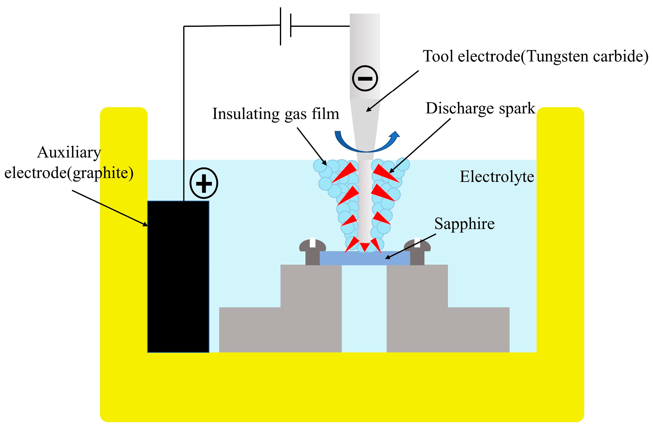
2. Experimental Principle
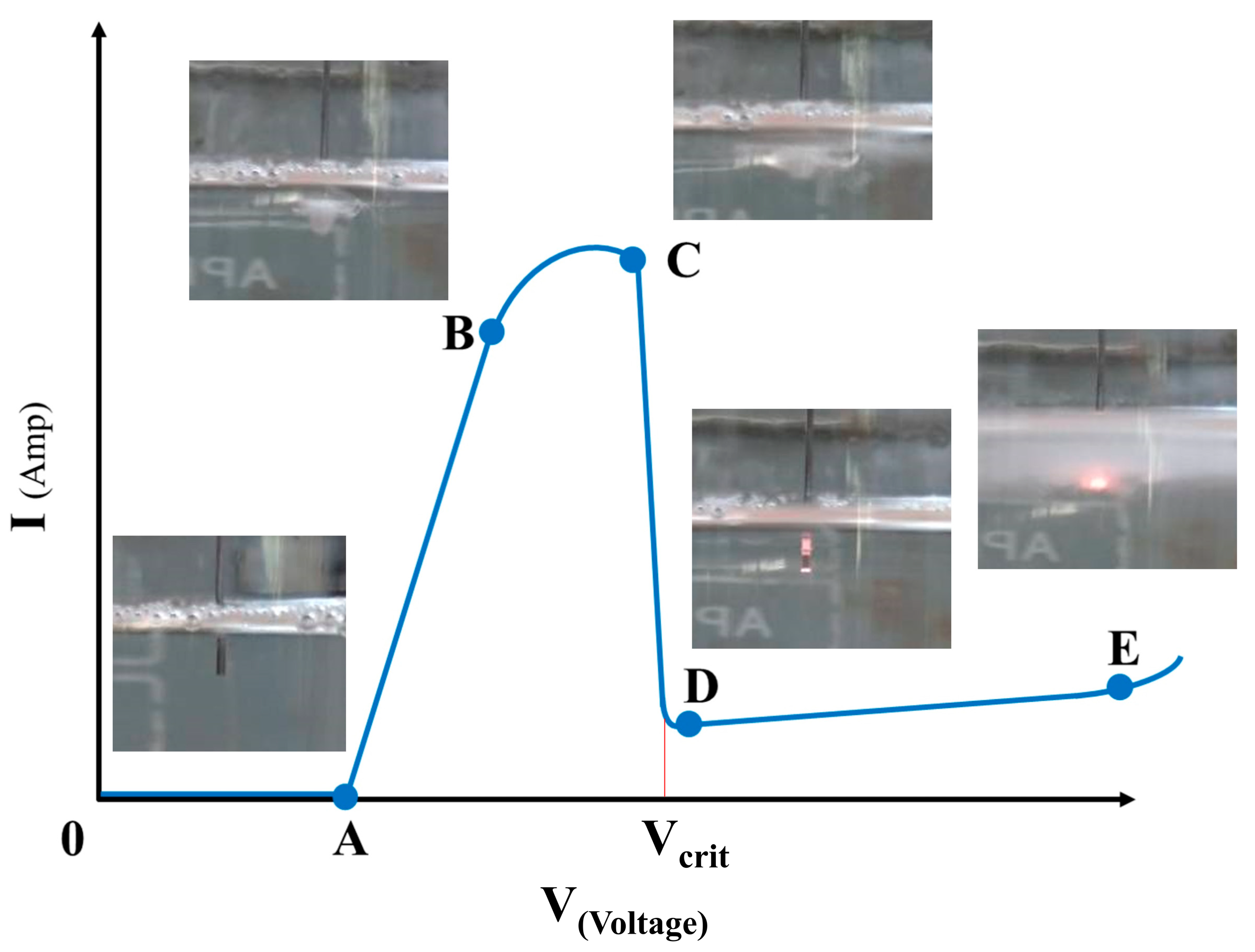
2.1. The Discharge-Spark Generation Mechanism of ECDM [24]
- Region 1 (0–A): the electrolytic current approaches zero, and there are no electrolytic bubbles generated on the electrode surface;
- Region 2 (A–B): the electrolytic bubble generation rate and current increase linearly as the voltage increases;
- Region 3 (B–C): A relatively non-dense gas film is formed on the surface of the tool electrode, which increases the resistance between the electrolyte interface and the tool electrode. At this time, the current is stable and does not increase as the voltage increases;
- Region 4 (C–D): A dense and fine gas film forms on the surface of the tool electrode, creating high electrical resistance between the electrolyte interface and the tool electrode. This causes the current of the original electrochemical circuit to approach zero, and the voltage at this point is called the critical voltage (Vcrit), as shown in Figure 2;
- Region 5 (D–E): the energy contained in the gas film collapses through the film as the voltage rises over the critical voltage, resulting in insulation breakdown and the spark-discharge phenomenon.
2.2. The Material Removal Mechanism of Electrochemical Discharge Machining
2.2.1. The Electrochemical Discharge Machining Mechanism [24]
2.2.2. Chemical Etching [25]
3. Experimental Setup
3.1. Experimental Material
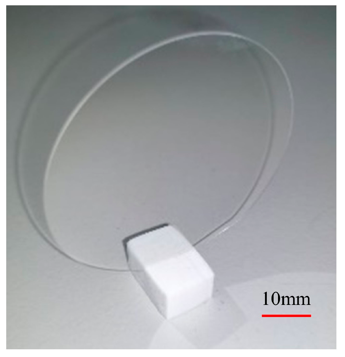
3.1.1. Sapphire Wafer Workpiece
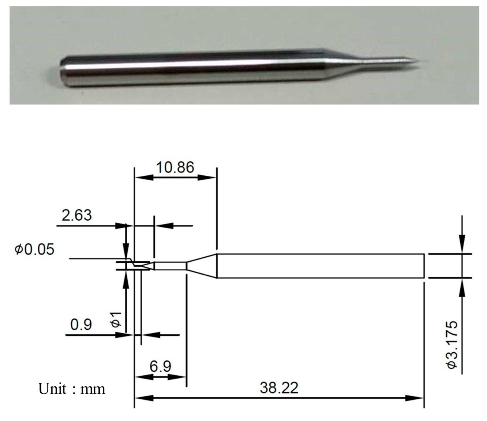
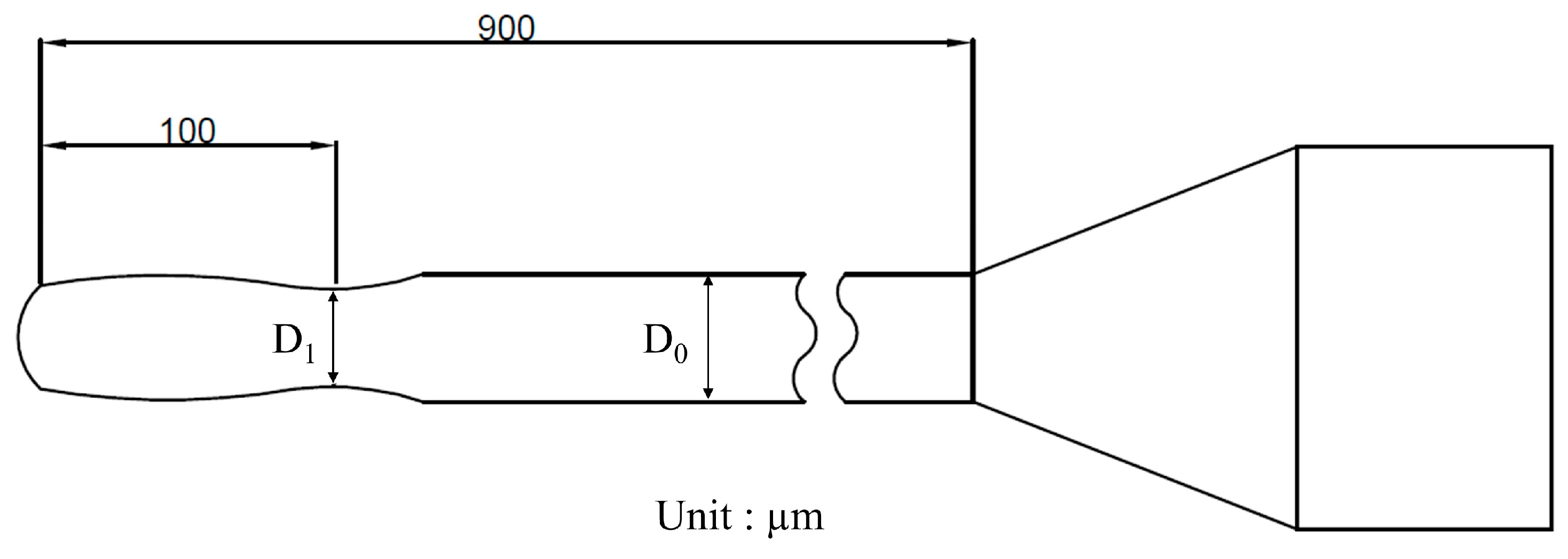
3.1.2. Cylindrical Tool Electrode
3.2. Experimental Setup
3.3. Experimental Parameters
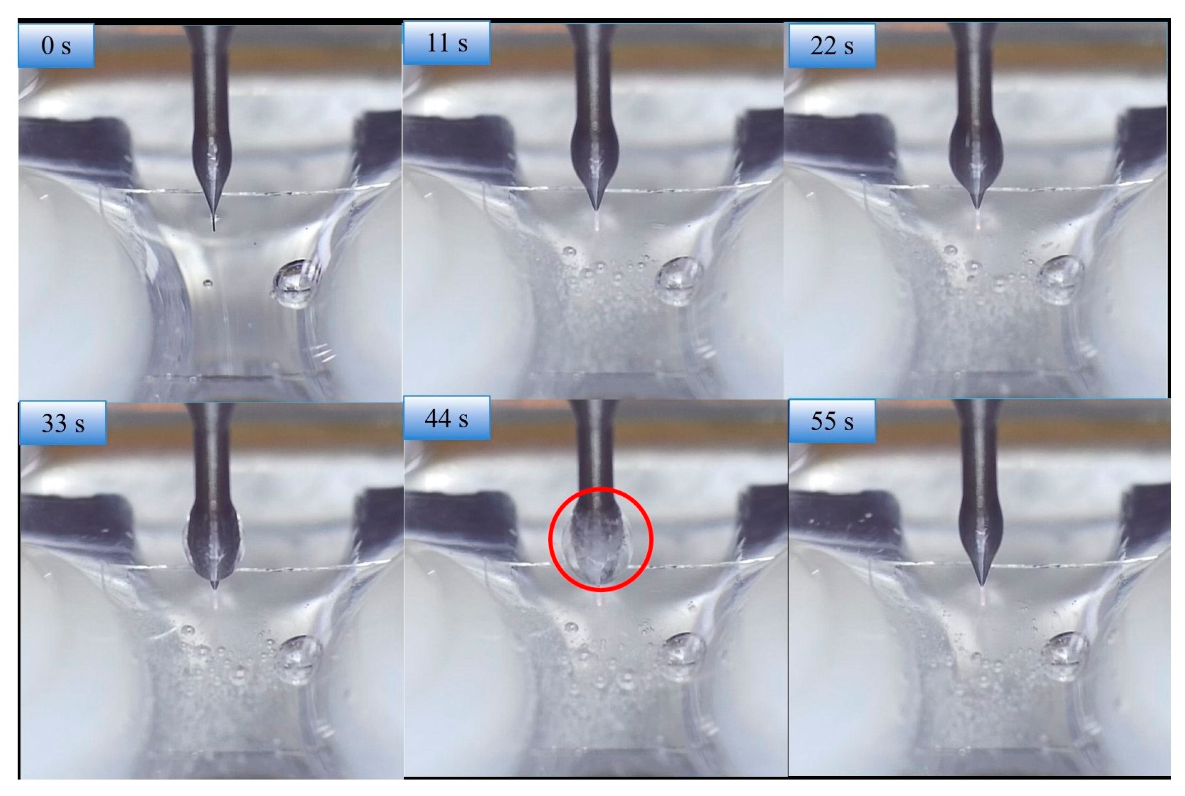
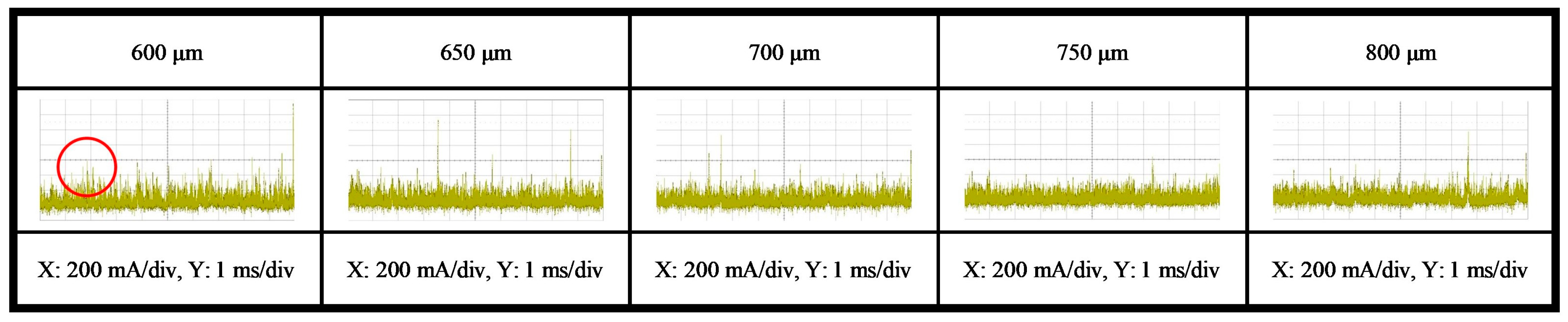
3.4. Experimental Measurement and Observation
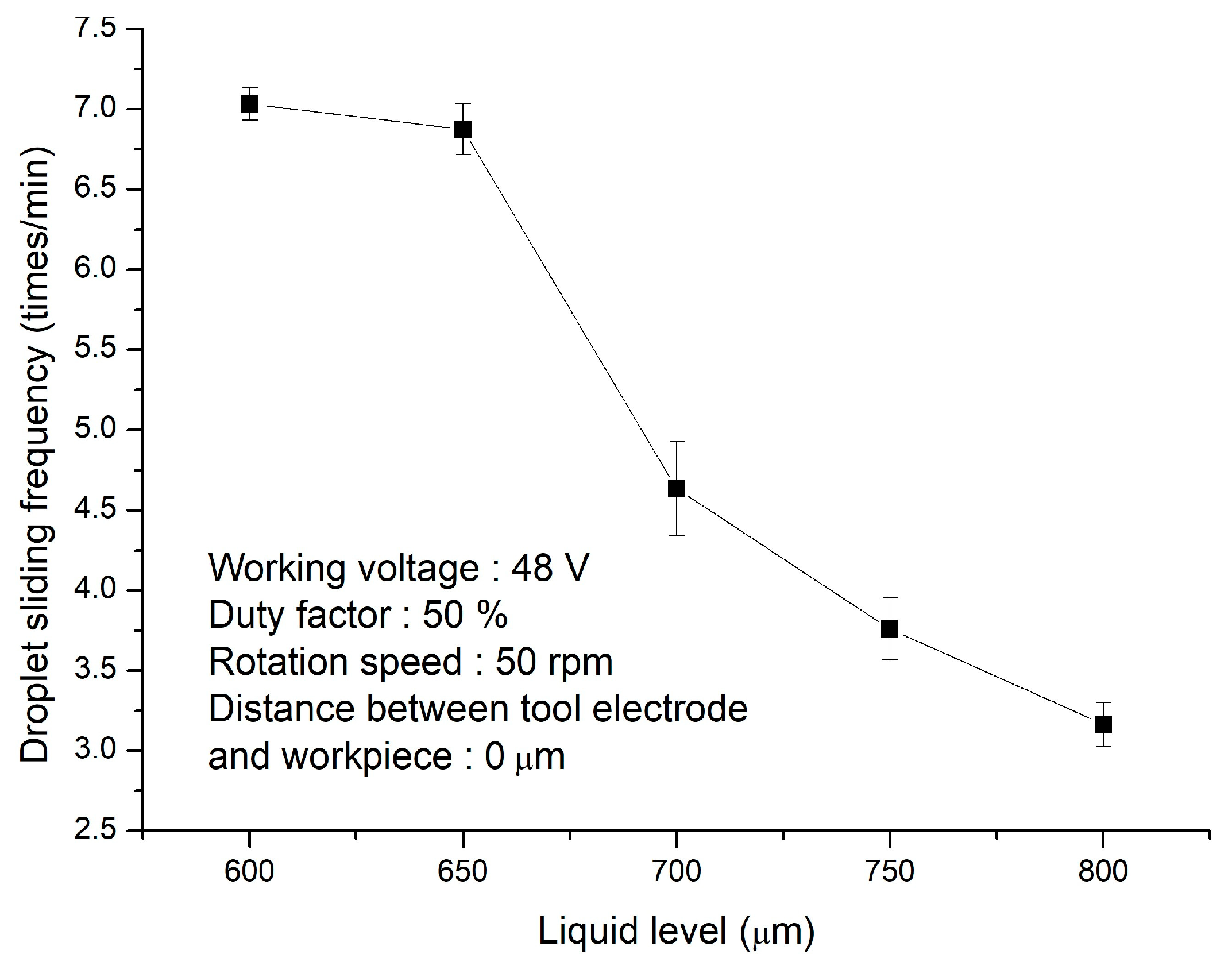
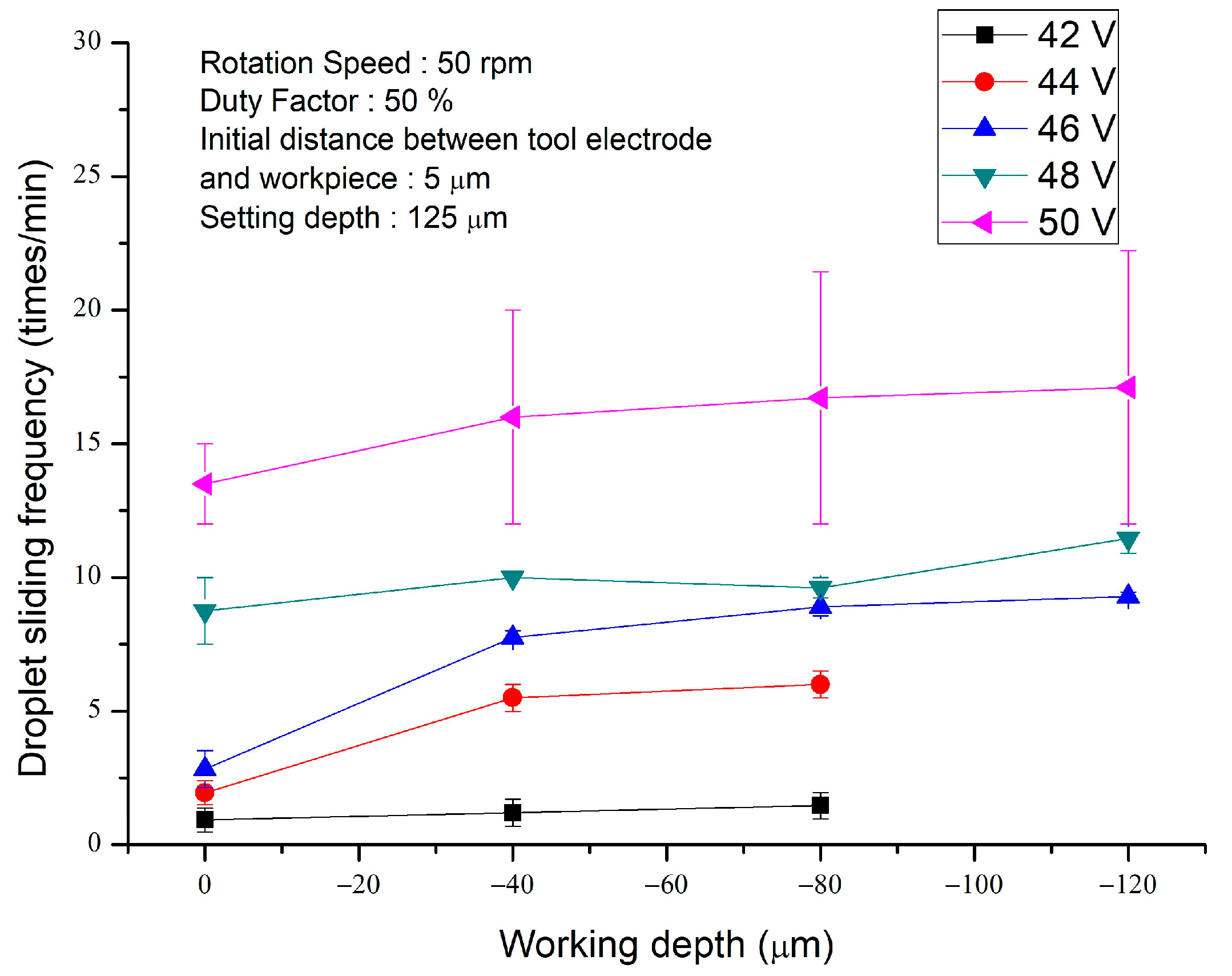
3.4.1. Droplet Sliding Frequency Measurement Method
3.4.2. Tool Electrode Wear Measurement Method
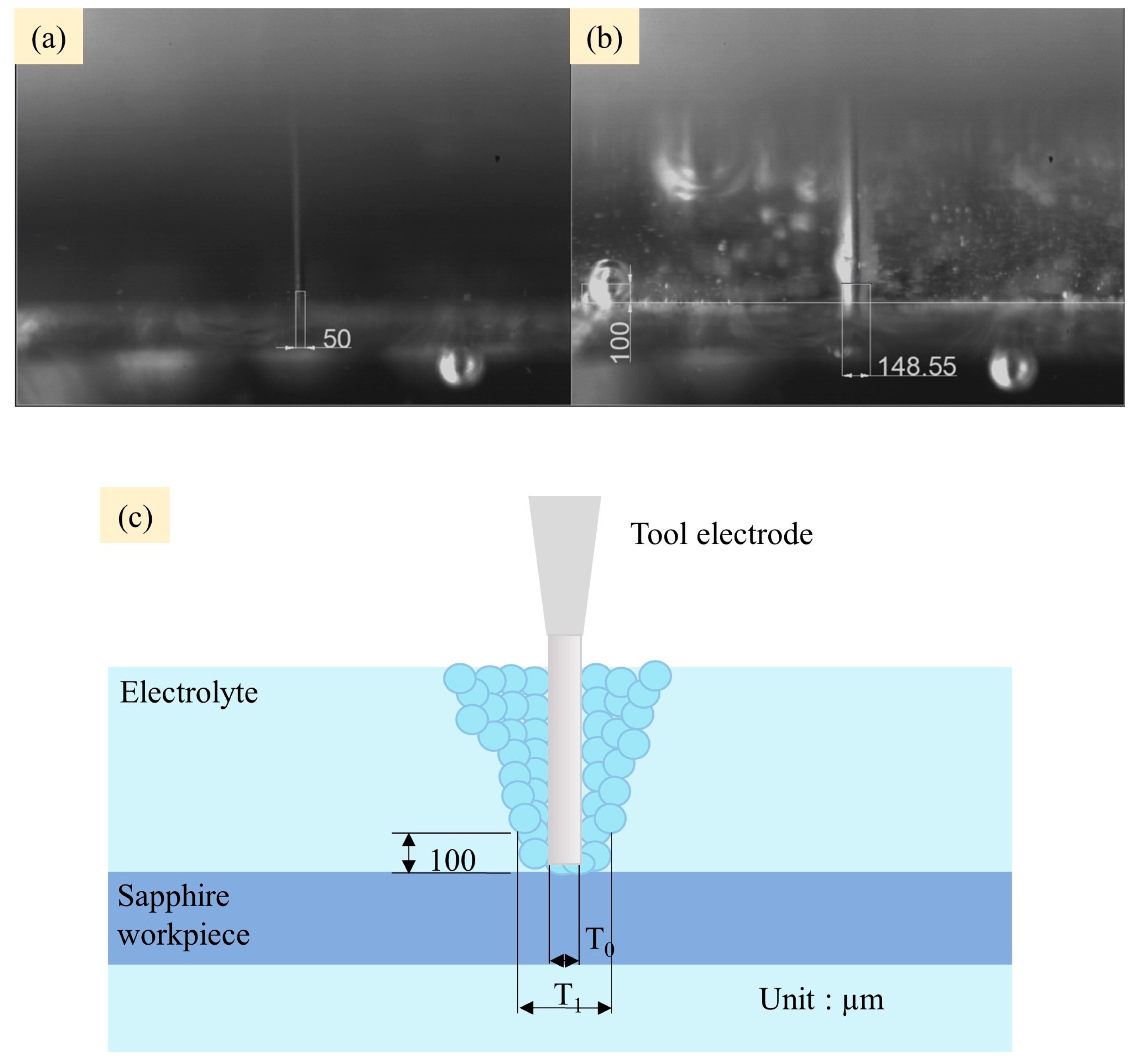
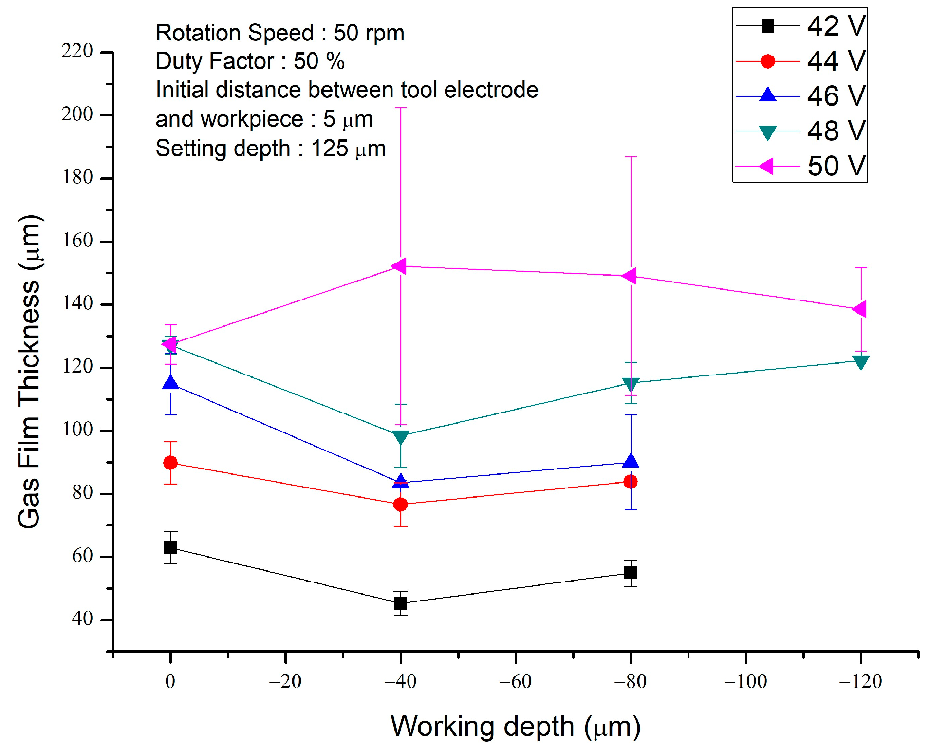
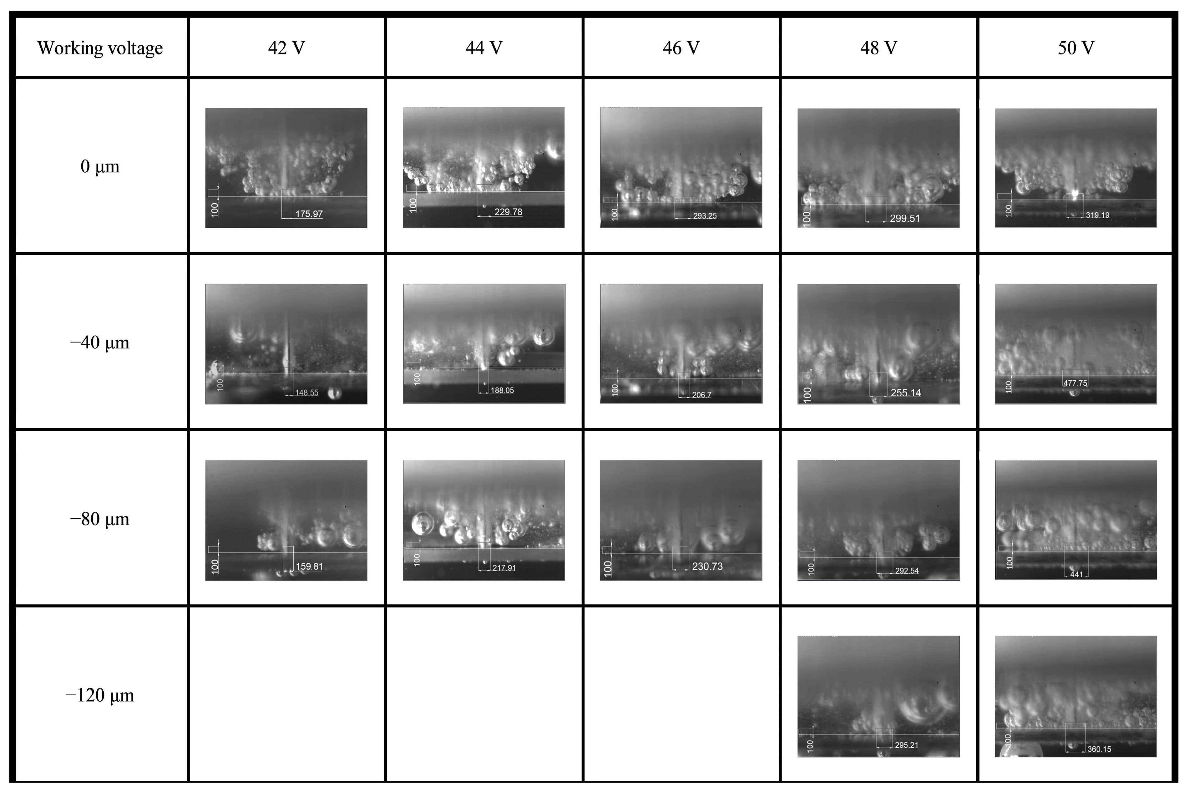
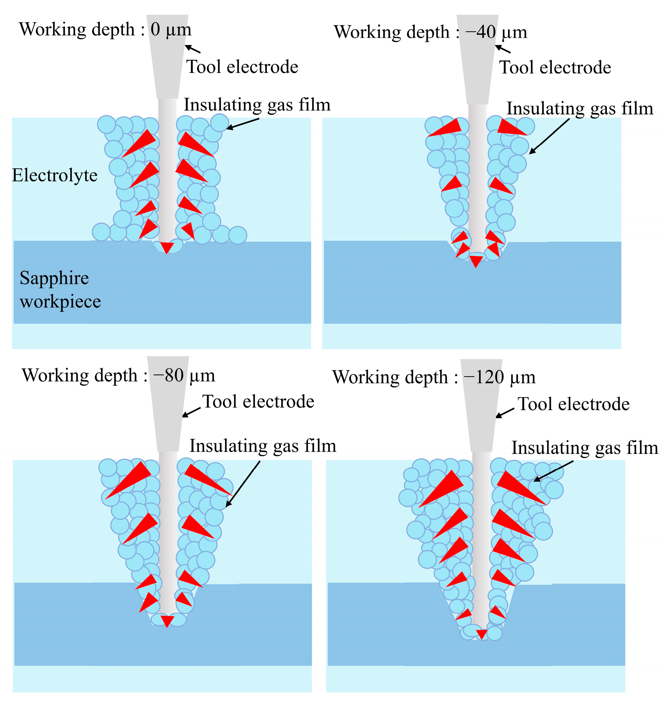
3.4.3. Gas-Film Thickness Measurement Method
4. Result and Discussion
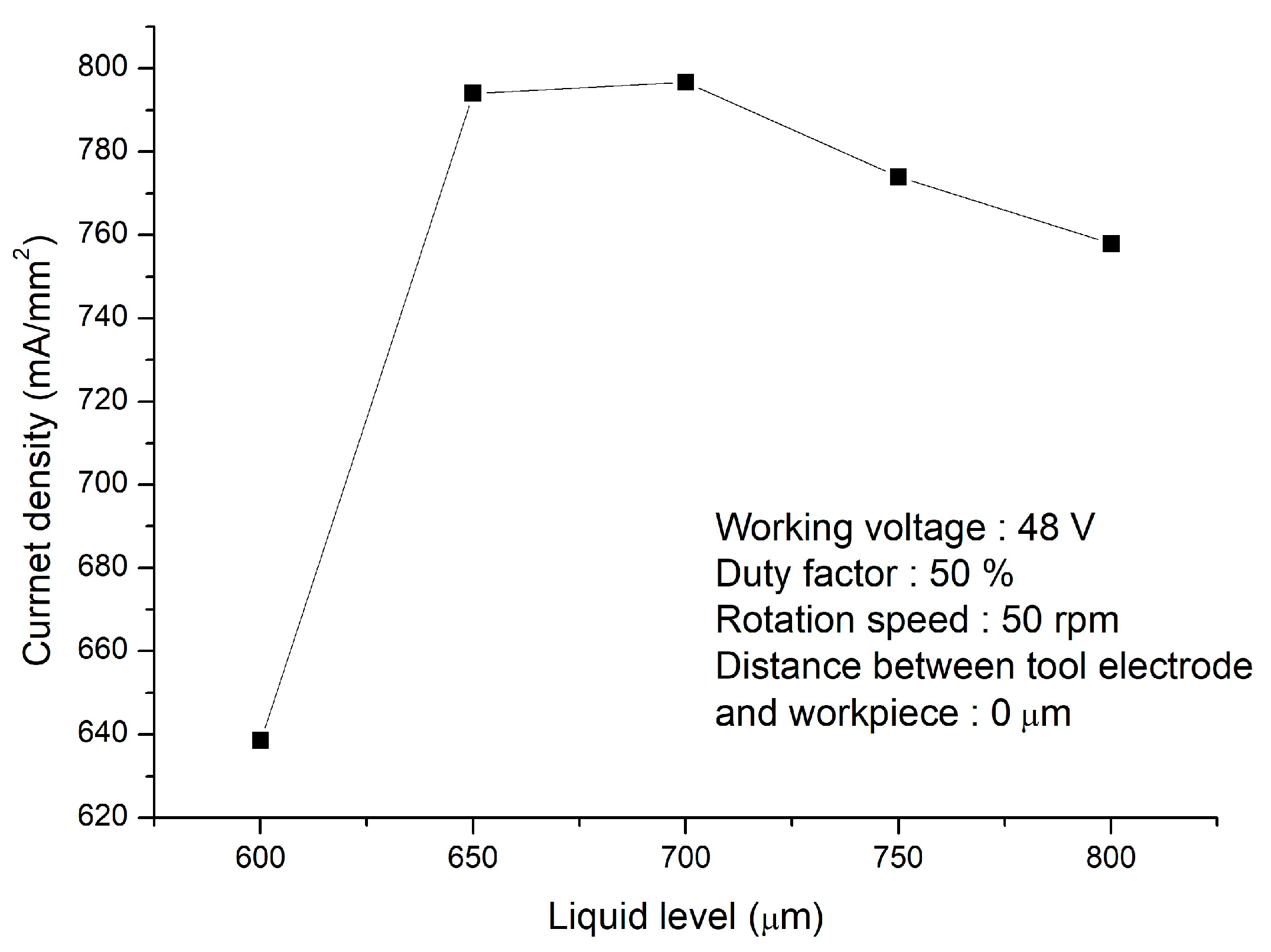
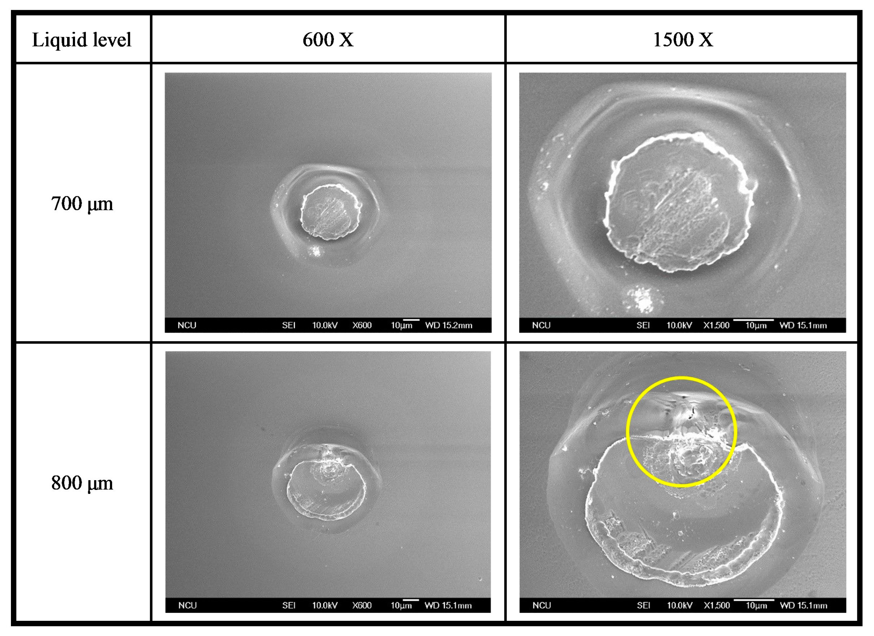
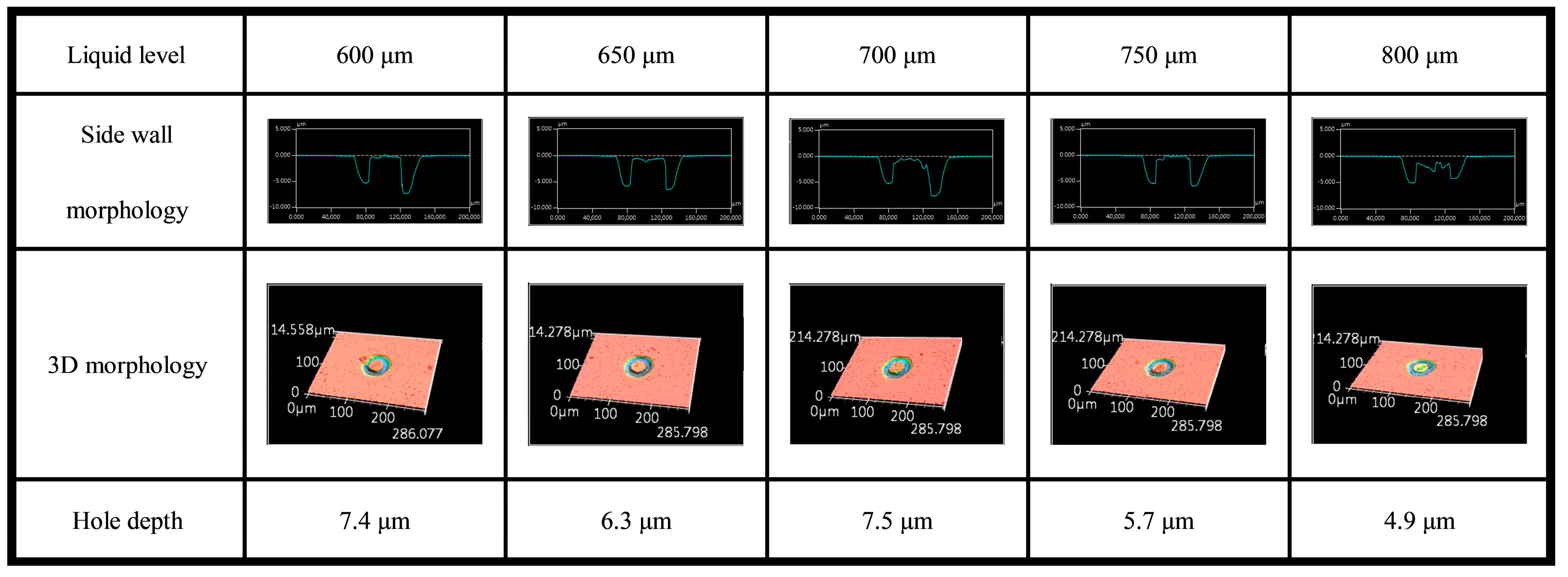
4.1. Effect of Liquid Level on Sapphire ECDM
4.2. Effects of Different Parameters on Sapphire ECDM
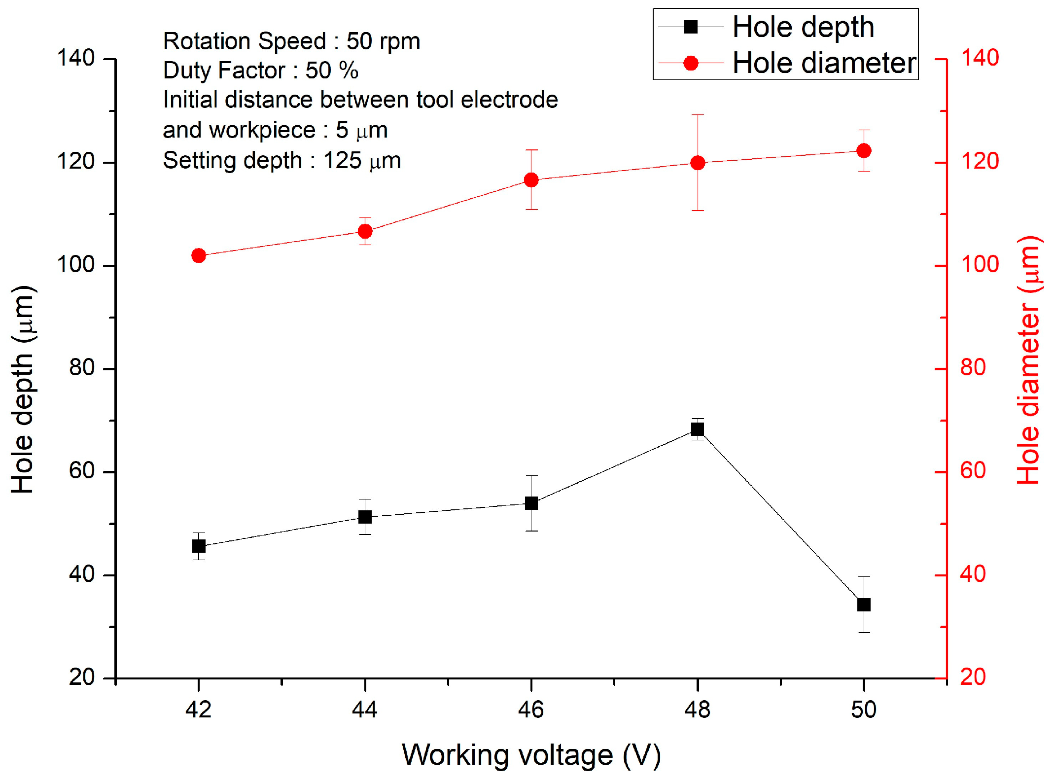
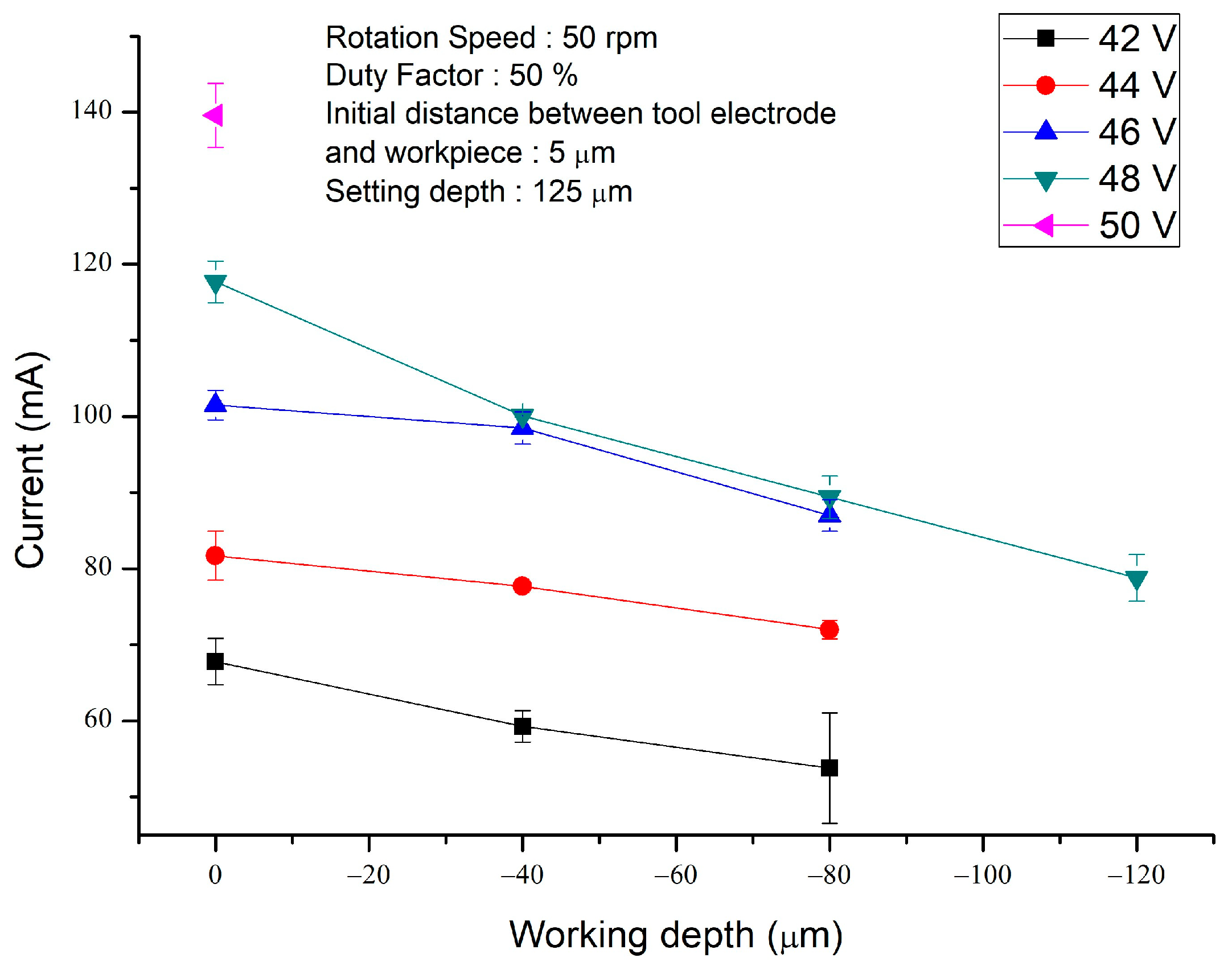
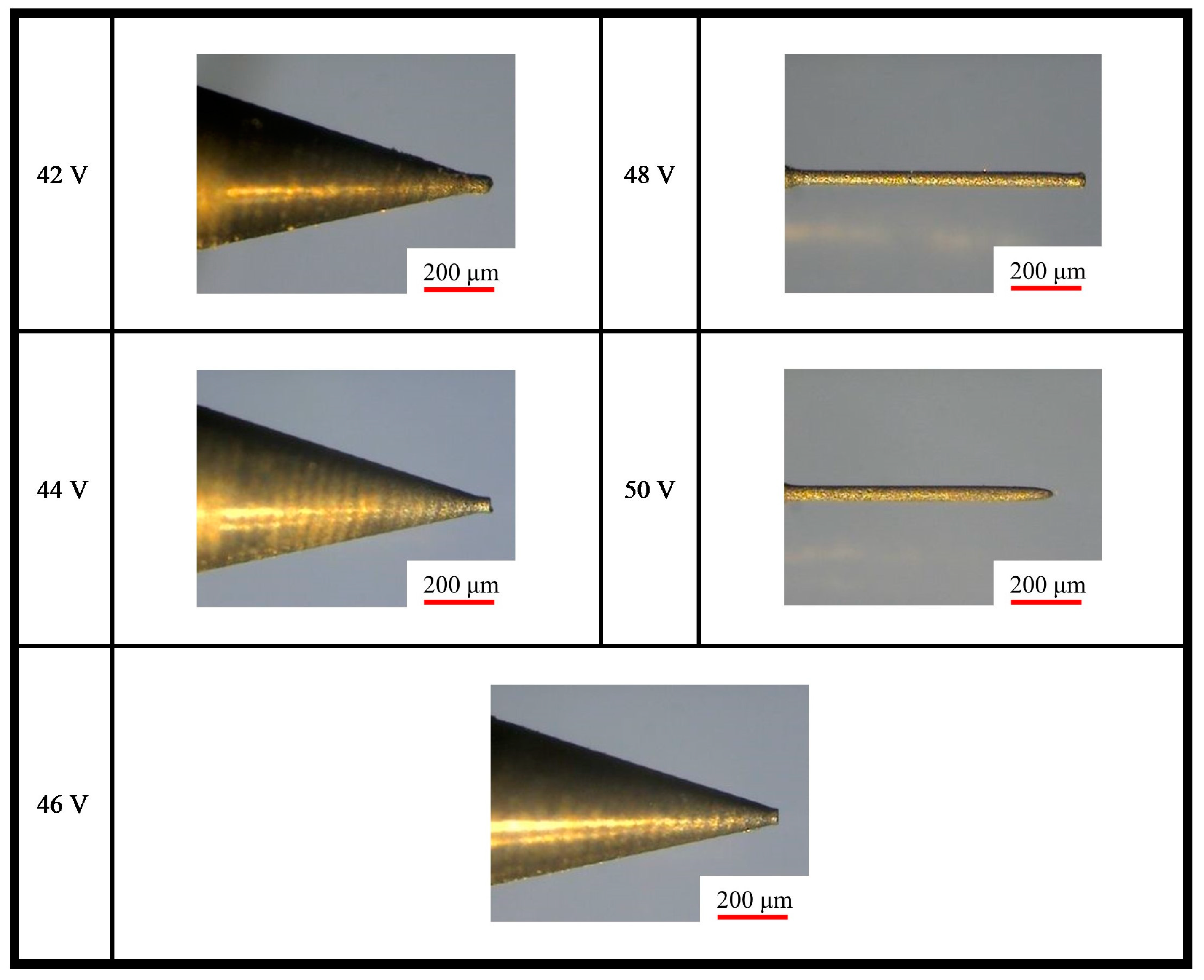
4.2.1. Effect of Different Working Voltage on Sapphire ECDM
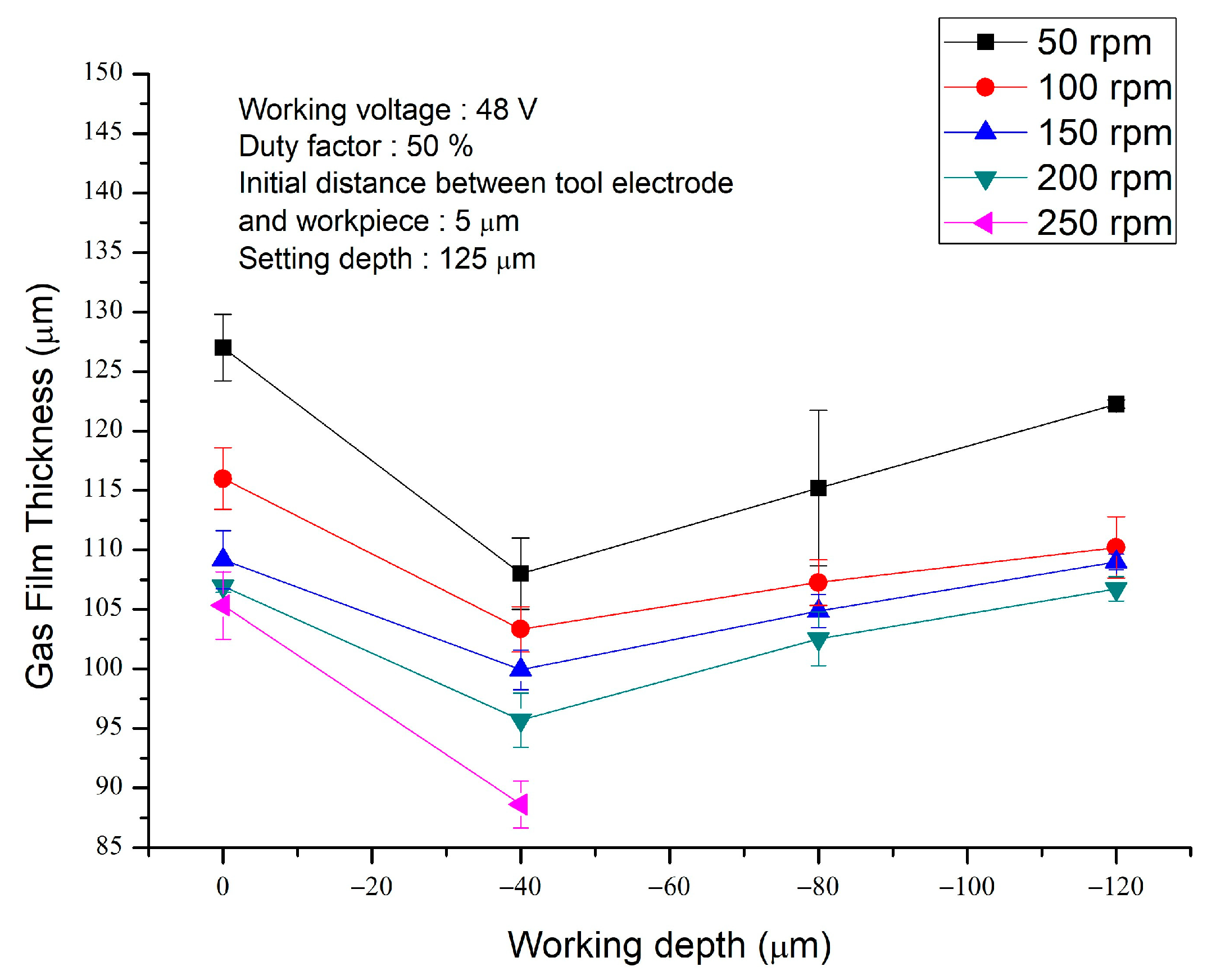
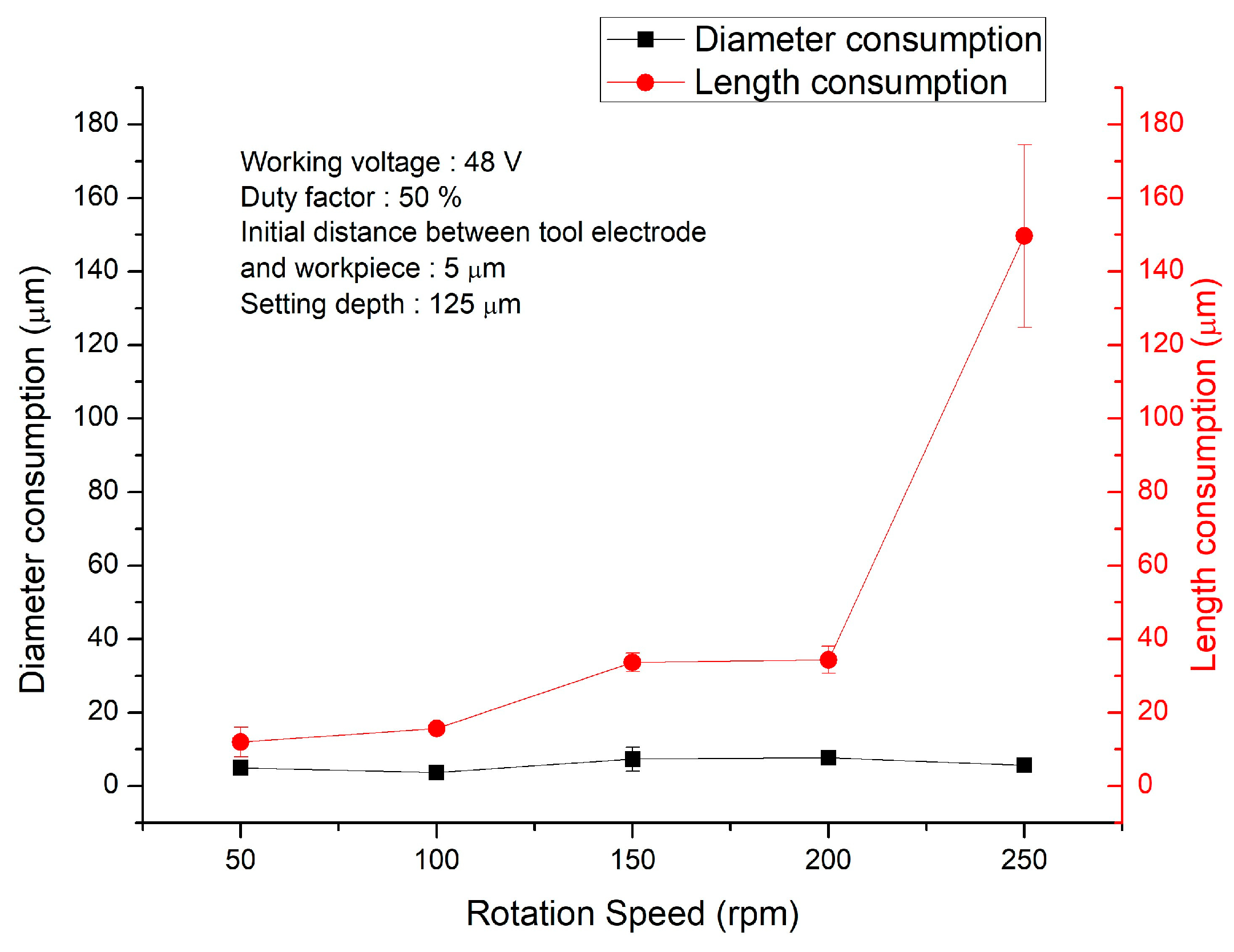
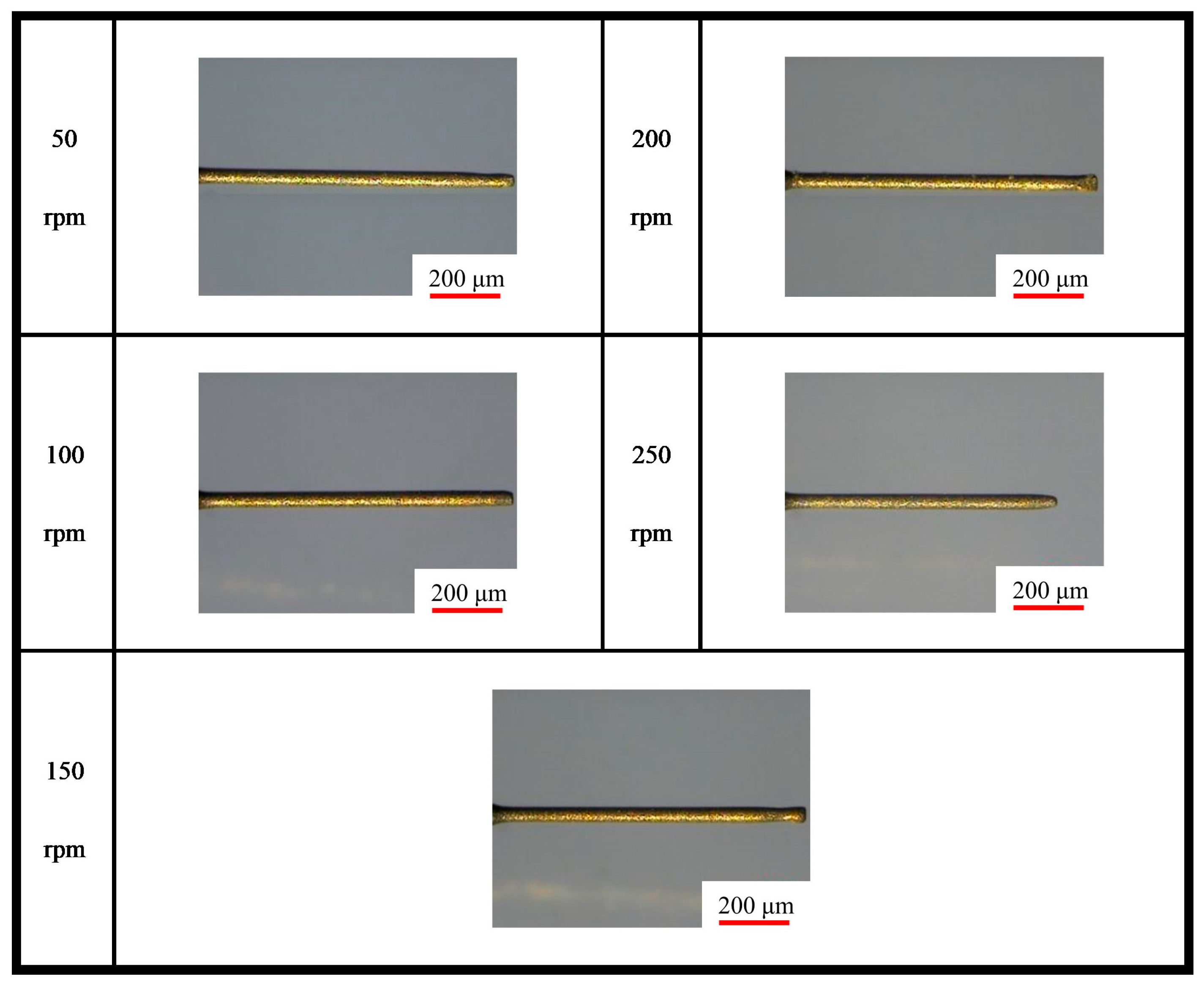
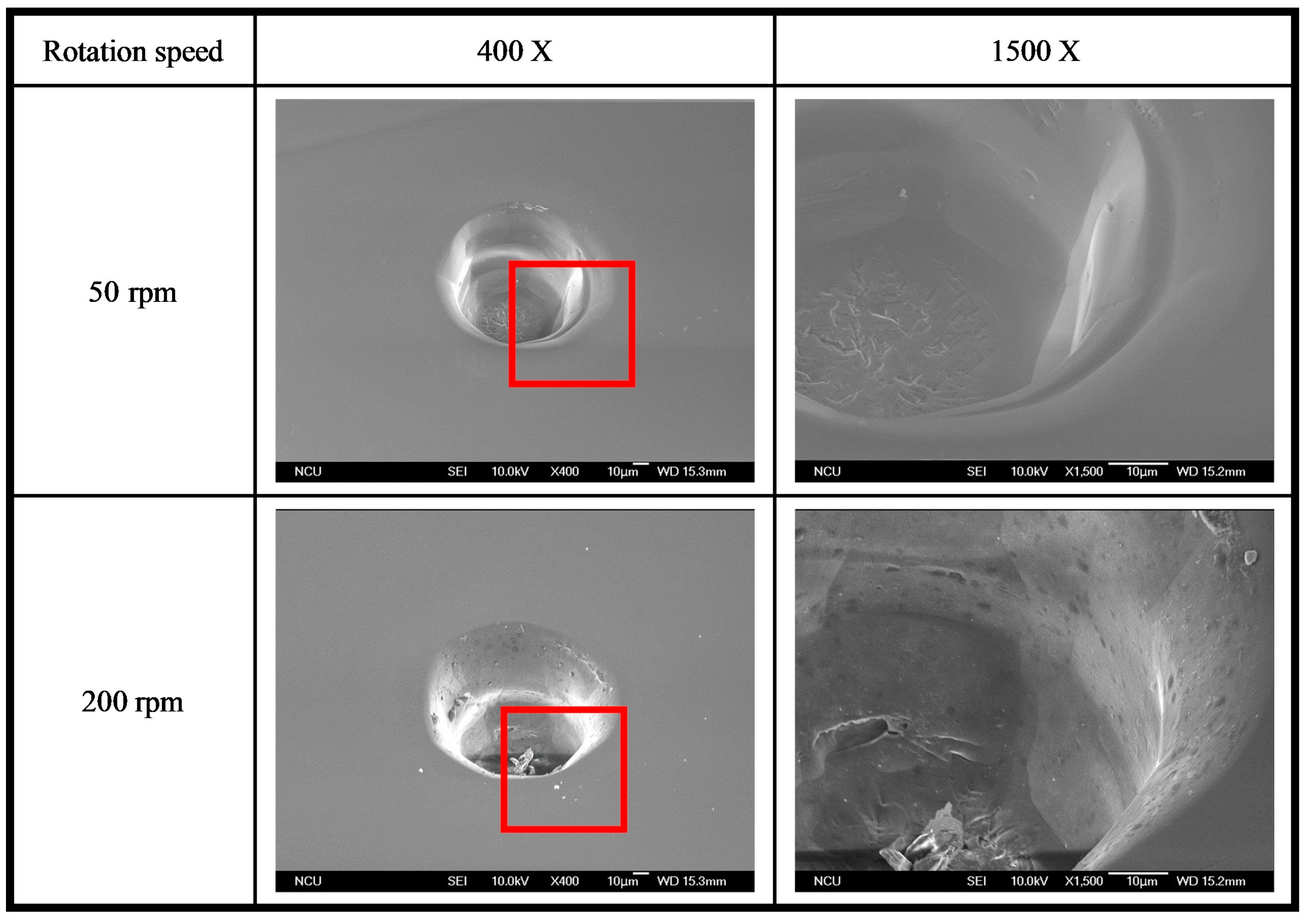
4.2.2. Effect of Different Rotation Speeds on Sapphire ECDM
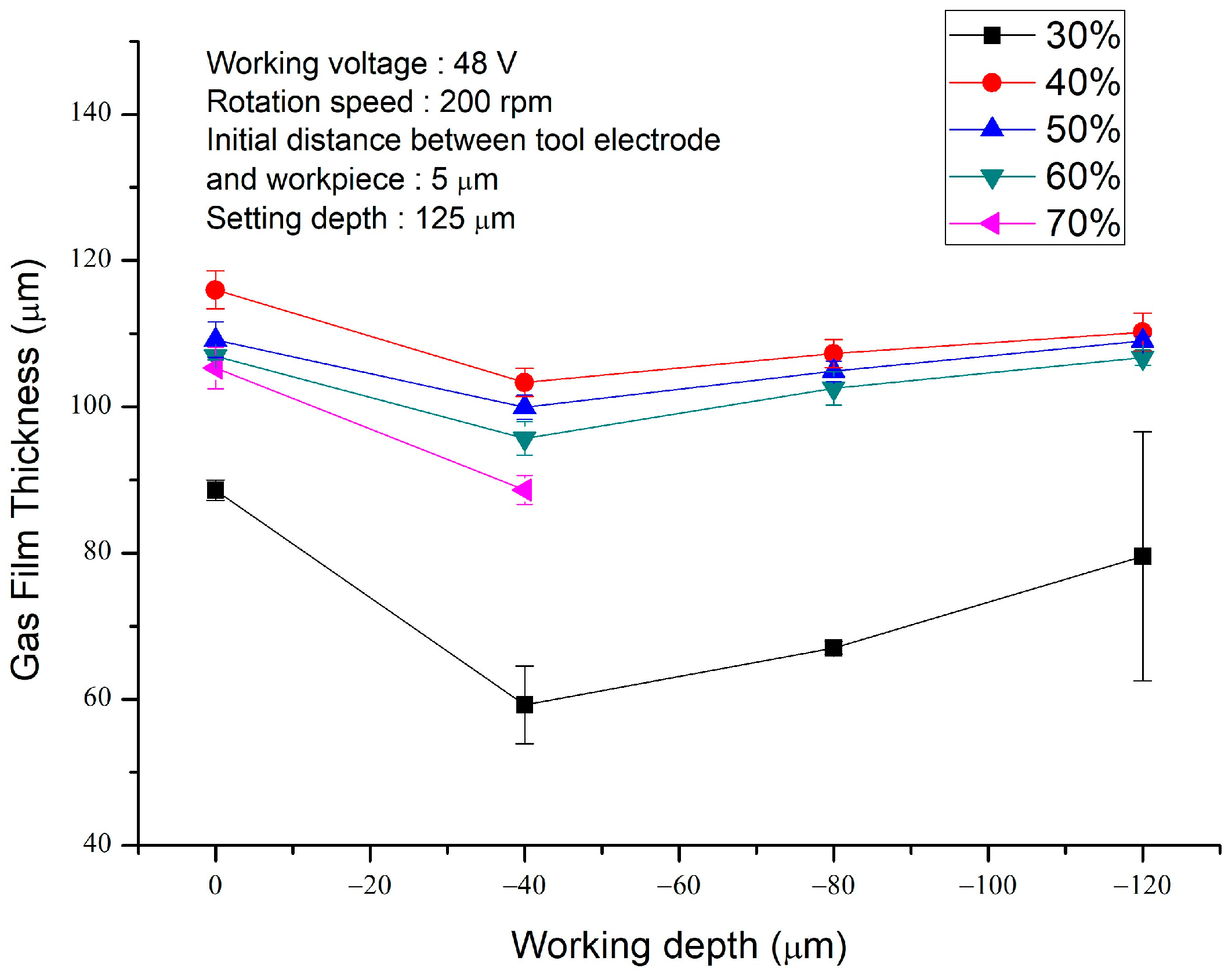
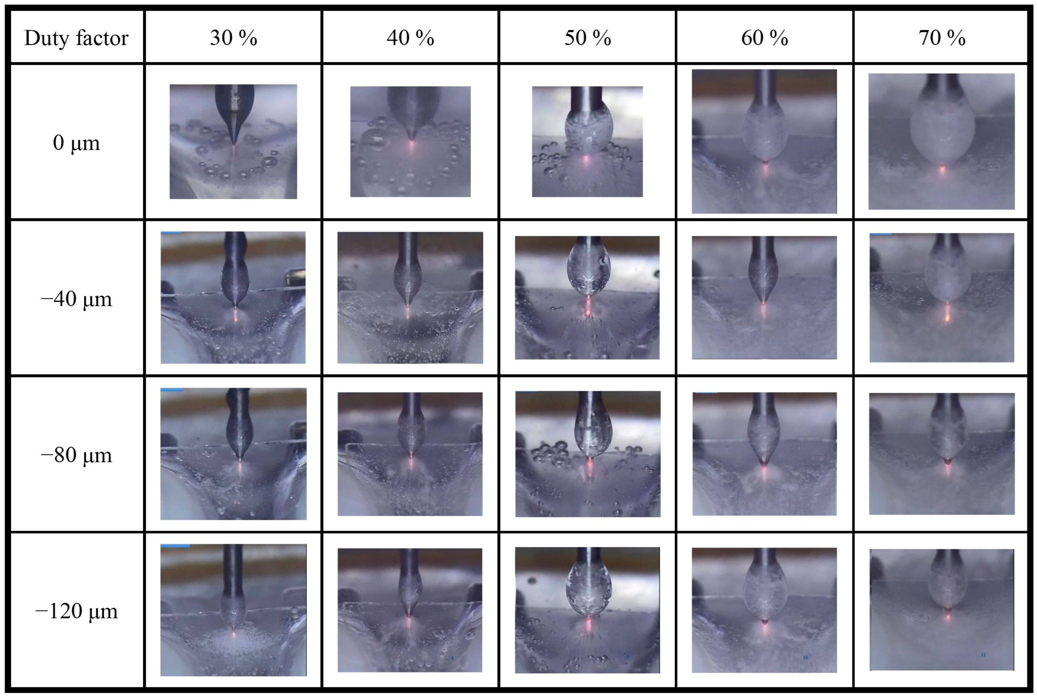
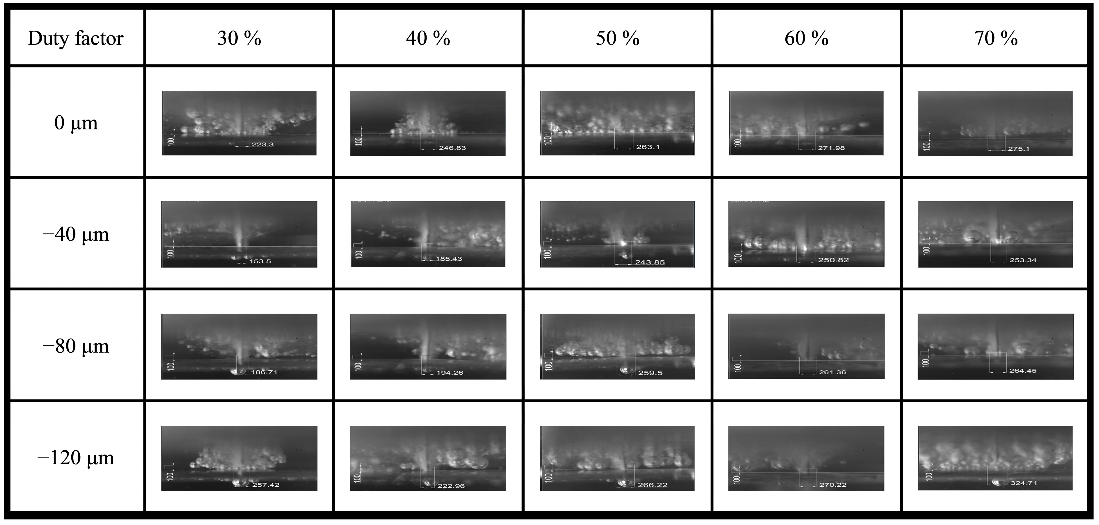
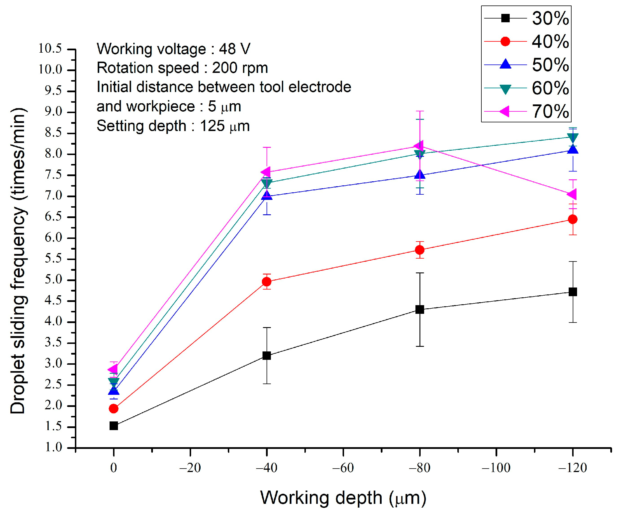
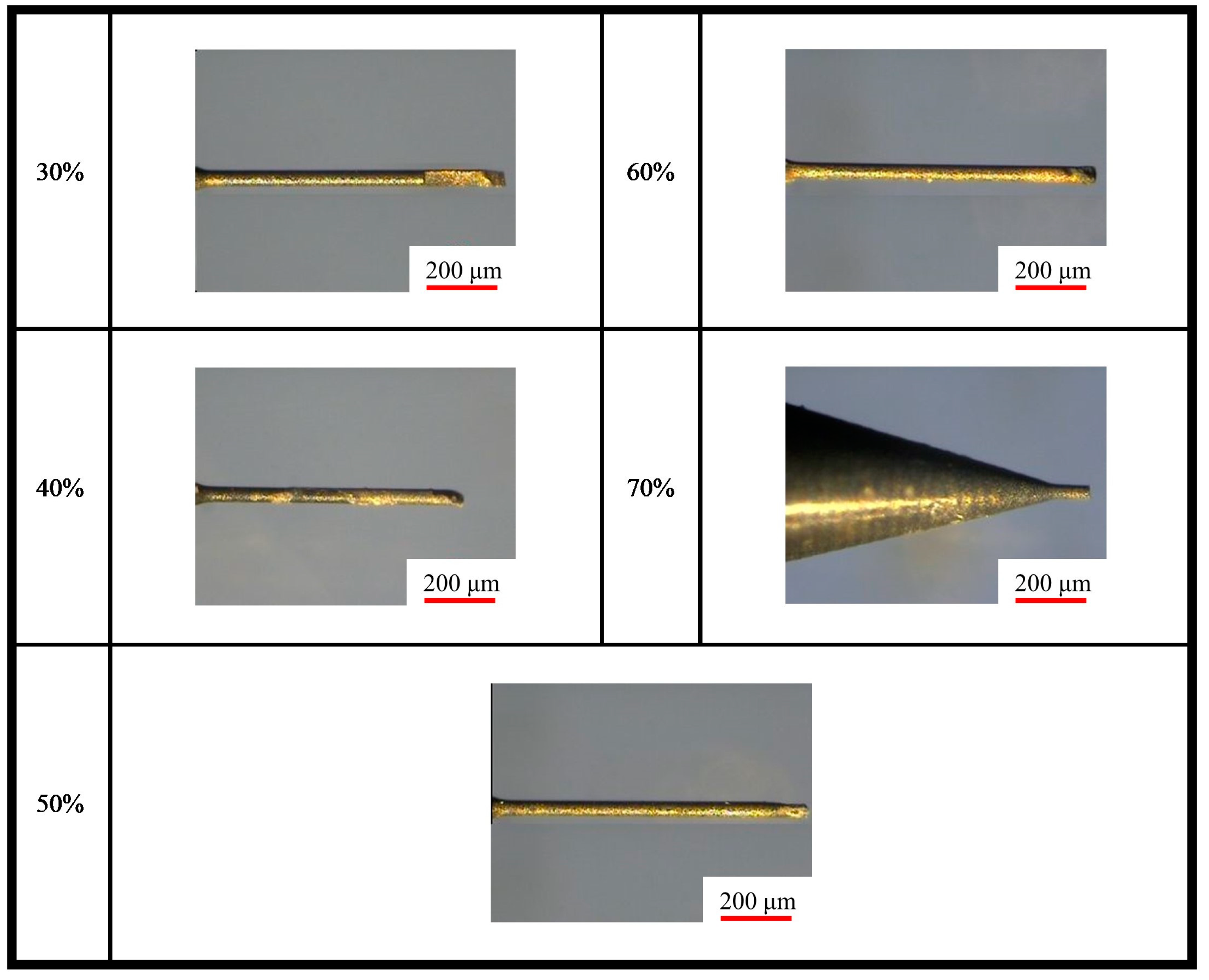
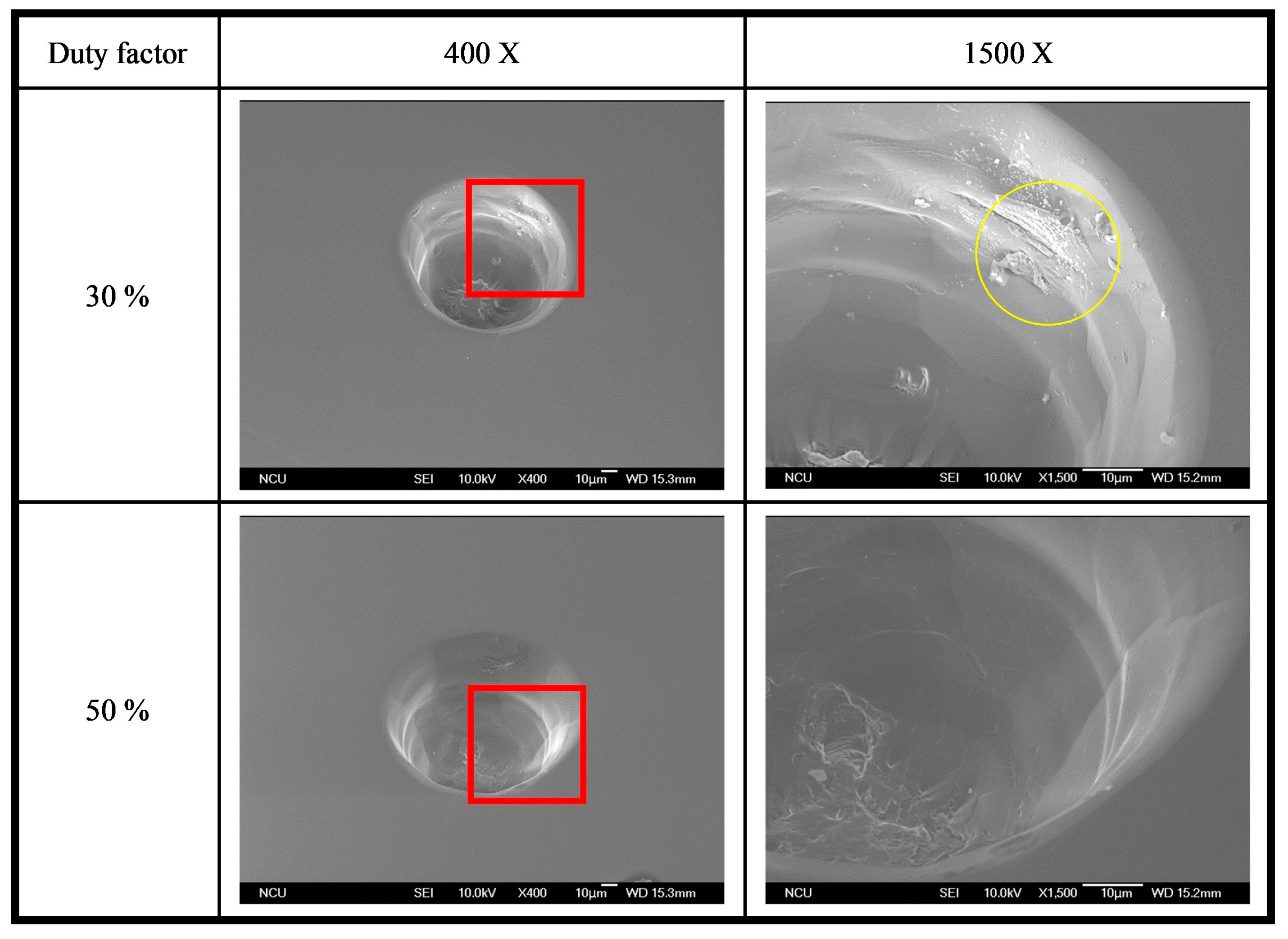
4.2.3. Effect of Different Duty Factors on Sapphire ECDM
5. Conclusions
- When the liquid level increased from 600 µm to 700 µm, the volume of the machined micro-holes increased with the rising liquid level. At this liquid level, the current density also increased with the liquid level. However, the current density began to decrease when the liquid level exceeded 700 µm, resulting in a reduction in the volume of the machined micro-holes with the increasing liquid level;
- When the working voltage was increased from 42 V to 48 V, the hole diameter and hole depth of the micro-holes increased with the higher working voltage. However, excessive wear at the tool electrode’s tip led to a significant decrease in machining efficiency when the working voltage was raised to 50 V, resulting in the shallowest hole depth;
- Under different rotational speeds, the hole diameter and hole depth of the micro-holes increased with the higher rotational speed. However, excessive wear at the tool electrode’s tip led to a significant decrease in the machining efficiency when the rotational speed was raised to 250 rpm, resulting in a decrease in the machining depth;
- As the duty factor increased from 30% to 50%, the hole diameter and hole depth also increased. However, excessive wear on the tool electrode occurred due to overly large discharge sparks when the duty factor was increased from 50% to 70%. As a result, the machining depth decreased with the increased duty factor.
- When the optimal machining parameters were used, including a liquid level of 700 µm, a working voltage of 48 V, a rotation speed of 200 rpm, and a duty factor of 50%, a hole diameter of 129.5 μm and an average machining depth of 86.7 μm were obtained.
Author Contributions
Funding
Data Availability Statement
Conflicts of Interest
References
- Bhattacharyya, B.; Doloi, B.N.; Sorkhel, S.K. Experimental Investigations into Electrochemical Discharge Machining (ECDM) of Non-Conductive Ceramic Materials. J. Mater. Process. Technol. 1999, 95, 145–154. [Google Scholar] [CrossRef]
- Wüthrich, R.; Hof, L.A.; Lal, A.; Fujisaki, K.; Bleuler, H.; Mandin, P.; Picard, G. Physical Principles and Miniaturization of Spark Assisted Chemical Engraving (SACE). J. Micromech. Microeng. 2005, 15, S268–S275. [Google Scholar] [CrossRef]
- Wüthrich, R.; Spaelter, U.; Bleuler, H. The Current Signal in Spark-Assisted Chemical Engraving (SACE): What Does It Tell Us? J. Micromech. Microeng. 2006, 16, 779–785. [Google Scholar] [CrossRef]
- Wüthrich, R.; Hof, L.A. The Gas Film in Spark Assisted Chemical Engraving (SACE)—A Key Element for Micro-Machining Applications. Int. J. Mach. Tools Manuf. 2006, 46, 828–835. [Google Scholar] [CrossRef]
- Hajian, M.; Razfar, M.R.; Movahed, S. An Experimental Study on the Effect of Magnetic Field Orientations and Electrolyte Concentrations on ECDM Milling Performance of Glass. Precis. Eng. 2016, 45, 322–331. [Google Scholar] [CrossRef]
- Appalanaidu, B.; Dvivedi, A. On Controlling of Gas Film Shape in Electrochemical Discharge Machining Process for Fabrication of Elliptical Holes. Mater. Manuf. Process. 2021, 36, 558–571. [Google Scholar] [CrossRef]
- Yang, C.T.; Ho, S.S.; Yan, B.H. Micro Hole Machining of Borosilicate Glass through Electrochemical Discharge Machining (ECDM). Key Eng. Mater. 2001, 196, 149–166. [Google Scholar] [CrossRef]
- Mediliyegedara, T.K.K.R.; De Silva, A.K.M.; Harrison, D.K.; McGeough, J.A. An Intelligent Pulse Classification System for Electro-Chemical Discharge Machining (ECDM)—A Preliminary Study. J. Mater. Process. Technol. 2004, 149, 499–503. [Google Scholar] [CrossRef]
- West, J.; Jadhav, A. ECDM Methods for Fluidic Interfacing through Thin Glass Substrates and the Formation of Spherical Microcavities. J. Micromech. Microeng. 2007, 17, 403–409. [Google Scholar] [CrossRef]
- Peng, W.Y.; Liao, Y.S. Study of Electrochemical Discharge Machining Technology for Slicing Non-Conductive Brittle Materials. J. Mater. Process. Technol. 2004, 149, 363–369. [Google Scholar] [CrossRef]
- Zheng, Z.-P.; Su, H.-C.; Huang, F.-Y.; Yan, B.-H. The Tool Geometrical Shape and Pulse-off Time of Pulse Voltage Effects in a Pyrex Glass Electrochemical Discharge Microdrilling Process. J. Micromech. Microeng. 2007, 17, 265–272. [Google Scholar] [CrossRef]
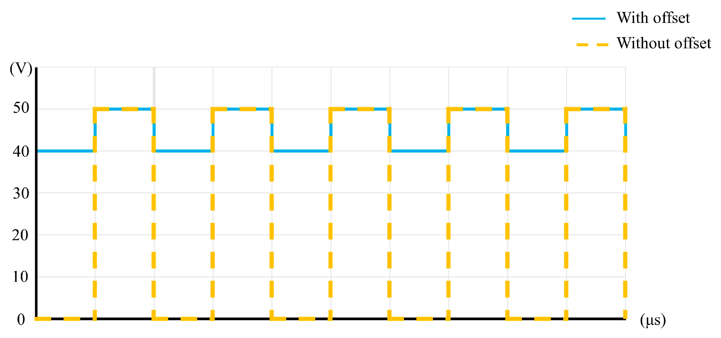
- Zheng, Z.-P.; Lin, J.-K.; Huang, F.-Y.; Yan, B.-H. Improving the Machining Efficiency in Electrochemical Discharge Machining (ECDM) Microhole Drilling by Offset Pulse Voltage. J. Micromech. Microeng. 2008, 18, 025014. [Google Scholar] [CrossRef]
- Kim, D.-J.; Ahn, Y.; Lee, S.-H.; Kim, Y.-K. Voltage Pulse Frequency and Duty Ratio Effects in an Electrochemical Discharge Microdrilling Process of Pyrex Glass. Int. J. Mach. Tools Manuf. 2006, 46, 1064–1067. [Google Scholar] [CrossRef]
- Han, M.-S.; Min, B.-K.; Lee, S.J. Geometric Improvement of Electrochemical Discharge Micro-Drilling Using an Ultrasonic-Vibrated Electrolyte. J. Micromech. Microeng. 2009, 19, 065004. [Google Scholar] [CrossRef]
- Cao, X.D.; Kim, B.H.; Chu, C.N. Micro-Structuring of Glass with Features Less than 100μm by Electrochemical Discharge Machining. Precis. Eng. 2009, 33, 459–465. [Google Scholar] [CrossRef]
- Tang, W.; Kang, X.; Zhao, W. Experimental Investigation of Gas Evolution in Electrochemical Discharge Machining Process. Int. J. Electrochem. Sci. 2019, 14, 970–984. [Google Scholar] [CrossRef]
- Jiang, B.; Lan, S.; Wilt, K.; Ni, J. Modeling and Experimental Investigation of Gas Film in Micro-Electrochemical Discharge Machining Process. Int. J. Mach. Tools Manuf. 2015, 90, 8–15. [Google Scholar] [CrossRef]
- Singh, M.; Singh, S. Electrochemical Discharge Machining: A Review on Preceding and Perspective Research. Proc. Inst. Mech. Eng. Part B J. Eng. Manuf. 2019, 233, 1425–1449. [Google Scholar] [CrossRef]
- Sabahi, N.; Razfar, M.R.; Hajian, M. Experimental Investigation of Surfactant-Mixed Electrolyte into Electrochemical Discharge Machining (ECDM) Process. J. Mater. Process. Technol. 2017, 250, 190–202. [Google Scholar] [CrossRef]
- Liu, Y.; Wei, Z.; Wang, M.; Zhang, J. Experimental Investigation of Micro Wire Electrochemical Discharge Machining by Using a Rotating Helical Tool. J. Manuf. Process. 2017, 29, 265–271. [Google Scholar] [CrossRef]
- Sundaram, M.; Chen, Y.-J.; Rajurkar, K. Pulse Electrochemical Discharge Machining of Glass-Fiber Epoxy Reinforced Composite. CIRP Ann. 2019, 68, 169–172. [Google Scholar] [CrossRef]
- Bian, J.; Ma, B.; Liu, X.; Qi, L. Experimental Study of Tool Wear in Electrochemical Discharge Machining. Appl. Sci. 2020, 10, 5039. [Google Scholar] [CrossRef]
- Rajput, V.; Goud, M.; Suri, N.M. Finite Element Modeling for Comparing the Machining Performance of Different Electrolytes in ECDM. Arab. J. Sci. Eng. 2021, 46, 2097–2119. [Google Scholar] [CrossRef]
- Chen, Y.; Feng, X.; Xin, G. Experimental Study on Ultrasonic Vibration-Assisted WECDM of Glass Microstructures with a High Aspect Ratio. Micromachines 2021, 12, 125. [Google Scholar] [CrossRef]
- Zhang, L.; Yuan, Z.; Jiang, S.; Shen, H.; Cao, F.; Ning, Z.; Huang, Y.; Xing, D.; Zuo, H.; Han, J.; et al. Cavity Etching Evolution on the A-Plane of Sapphire Crystal in Molten KOH Etchant. J. Cryst. Growth 2020, 552, 125926. [Google Scholar] [CrossRef]


| Items | Dimensions |
|---|---|
| Tool electrode holder diameter (mm) | 3.175 |
| Tool electrode diameter (mm) | 0.05 |
| Tool electrode length (mm) | 0.9 |
| Parameter | Description |
|---|---|
| Liquid level (µm) | 600, 650, 700, 750, 800 |
| Working voltage (V) | 42, 44, 46, 48, 50 |
| Rotation speed (rpm) | 50, 100, 150, 200, 250 |
| Duty factor (%) | 30, 40, 50, 60, 70 |
| Parameter | Setting Value |
|---|---|
| Total feeding stroke (µm) | 125 |
| Feed rate (µm/min) | 8 |
| Electrode diameter (µm) | 50 |
| Electrolyte | KOH |
| Electrolyte concentration (M) | 7 |
| Pulse duration (µs) | 10 |
| Auxiliary electrode | Graphite |
| Tool electrode | Tungsten carbide |
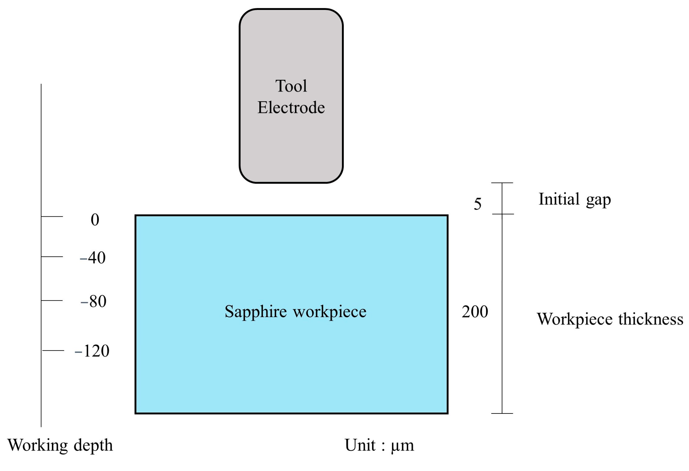
| Initial gap (µm) | 5 |
| Workpiece thickness (µm) | 200 |
| Distance between Auxiliary electrode and tool electrode (mm) | 80 |
Disclaimer/Publisher’s Note: The statements, opinions and data contained in all publications are solely those of the individual author(s) and contributor(s) and not of MDPI and/or the editor(s). MDPI and/or the editor(s) disclaim responsibility for any injury to people or property resulting from any ideas, methods, instructions or products referred to in the content. |
© 2024 by the authors. Licensee MDPI, Basel, Switzerland. This article is an open access article distributed under the terms and conditions of the Creative Commons Attribution (CC BY) license (https://creativecommons.org/licenses/by/4.0/).
Share and Cite
Yang, C.-H.; Yu, S.-H.; Tsui, H.-P. Observation of Gap Phenomena and Development Processing Technology for ECDM of Sapphire. Processes 2024, 12, 1149. https://doi.org/10.3390/pr12061149
Yang C-H, Yu S-H, Tsui H-P. Observation of Gap Phenomena and Development Processing Technology for ECDM of Sapphire. Processes. 2024; 12(6):1149. https://doi.org/10.3390/pr12061149
Chicago/Turabian StyleYang, Chun-Hao, Shao-Hua Yu, and Hai-Ping Tsui. 2024. "Observation of Gap Phenomena and Development Processing Technology for ECDM of Sapphire" Processes 12, no. 6: 1149. https://doi.org/10.3390/pr12061149