Article

Production of High-Power Nitrogen Sputtering Plasma for TiN Film Preparation

1
Department of Systems Innovation Engineering, Faculty of Science and Engineering, Iwate University, Morioka 020-8551, Iwate, Japan
2
Agri-Innovation Center, Iwate University, Morioka 020-8550, Iwate, Japan
*
Author to whom correspondence should be addressed.
Processes 2024, 12(7), 1314; https://doi.org/10.3390/pr12071314
Submission received: 10 April 2024 / Revised: 2 June 2024 / Accepted: 22 June 2024 / Published: 25 June 2024
(This article belongs to the Special Issue Plasma Science and Plasma-Assisted Applications)

Abstract

:
High-density nitrogen plasma was produced using a high-power pulsed power modulator to sputter titanium targets for the preparation of titanium nitride film. The high-power pulsed sputtering discharge unit consisted of two targets facing each other with the same electrical potential. The titanium target plates were used as target materials with dimensions of 60 mm length, 20 mm height, and 5 mm thickness. The gap length was set to be 10 mm. The magnetic field was created with a permanent magnet array behind the targets. The magnetic field strength at the gap between the target plates was 70 mT. The electrons were trapped by the magnetic and electric fields to enhance the ionization in the gap. The nitrogen and argon gases were injected into the chamber with 4 Pa gas pressure. The applied voltage to the target plates had an amplitude from −600 V to −1000 V with 600 μs in pulse width. The target current was approximately 10 A with the consumed power of 13 kW. The discharge sustaining voltage was almost constant and independent of the applied voltage, in the same manner as the conventional normal glow discharge. The ion density and electron temperature at the surface of the ionization region were obtained as 1.7 × 10¹⁹ m−3 and 3.4 eV, respectively, by the double probe measurements. The vertical distribution of ion density and electron temperature ranged from 1.1 × 10¹⁷ m−3 (at 6 cm from the target edge) to 1.7 × 10¹⁹ m−3 and from 2.4 eV (at 6 cm from the target edge) to 3.4 eV, respectively. From the emission spectra, the intensities of titanium atoms (Ti I), titanium ions (Ti II), and nitrogen ions (N2+) increased with increasing input power. However, the intensities ratio of Ti II to Ti I was not affected by the intensities from N2+.

1. Introduction

Surface modification of materials such as metals, ceramics, and polymers through the ion process is actively used in the material industry for various applications [1,2]. In the surface modification process, physical vapor deposition (PVD) and chemical vapor deposition (CVD) are mainly used to achieve the demand for the material in various applications. In the PDV process, steady-state ion sources such as vacuum arc discharge and magnetron sputtering (MS) are frequently used because they have outstanding properties such as high dose ion flux, etc. [3,4,5]. However, these ion sources have some disadvantages, e.g., the generation of droplets in the case of the vacuum arc discharge [6] and the limitation of power density less than 0.05 kW cm−2 in the direct current MS (dcMS) case [7,8]. To overcome the disadvantage of the dcMS, the MS is sometimes driven by the pulsed voltage. The pulse dcMS is used to control the heat flux from MS plasma toward the target material by controlling a duty factor [1]. High-power impulse magnetron sputtering (HiPIMS) was developed to increase ion process performance compared with that of the pulse dcMS. The typical performance of the HiPIMS is expressed as a short-term application of high-power density (1 kW cm−2 or more) with a large current (1 A cm−2 or more) on the target surface [9,10,11,12,13]. In HiPIMS, the ionization rate of sputtered metals reaches more than 60%, which is much higher than that of the dcMS and the pulse dcMS [1].
Several types of high-power glow discharge plasmas have been proposed and developed to satisfy the demand for the ion process, such as high density, no droplets, and uniform distribution. For example, the planar-type MS was proposed, and its performance was evaluated [4,14]. In the planar-type MS, permanent magnets are used to confine the plasma and are placed on the backside of the target to create a magnetic field in the vicinity of the target surface [15]. A shunting arc was also originally proposed and developed by Yukimura as an ion source by flowing a current of several kiloamperes through a conductive rod [16,17,18]. An inductively coupled plasma (ICP) has been widely used in the plasma processing industry as an ion source. ICP was also used by combining the HiPIMS to improve the ionization ratio of sputtered metals [19,20,21]. ICP was sometimes driven by the burst-type radio frequency of several hundred kilohertz to produce a high-density plasma (1019 m−3 or more) as an ion source [20,21]. Hollow cathode discharges (HCD) were developed to produce high-density plasma [22,23]. In the HCD, electrons are trapped in the hollow cathode, such as a hollow cylinder, between two parallel plates, etc. [24,25]. The HCD was used by combining the HiPIMS pulsed moderator to improve an ion process performance [26]. Moreover, the parallel plates HCD monology was combined with magnetic plasma confinement to produce metal ions through the sputtering process. This system consists of a pair of facing targets set perpendicular to the direction of the magnetic field [27,28,29].
The magnetic confinement-facing targets were developed and driven by a high-power pulse modulator to improve the ionization rate of sputtered metal particles [30]. This high-power pulsed sputtering (HPPS) system is categorized as a kind of HiPIMS; however, it has unique characteristics due to its unique configuration of the targets and magnetic field distribution. After the plasma ignition between the pair of the target plates, the cathode fall region is formed in the vicinity of the target plates because the target plates have negative potential by applying negative voltage from the high-power pulse modulator. The electrons are trapped by the Lorenz force with the electric potential gradient, and the magnetic field is produced by the external permanent magnets. As a result, the plasma is confined in the gap [31]. Moreover, the HPPS has advantages compared to the vacuum arc, such as being droplet-free, because the glow discharge plasma is confined in the gap without arcing [32]. The HPPS showed an instantaneous power consumption of 45 kW with a power density of 2.5 kW cm−2 [33]. The plasma density of the HPPS was obtained as 3 × 10¹⁸ m−3 in the vicinity of the targets [34]. The HPPS was employed for the preparation of diamond-like carbon (DLC) films [35] and titanium carbon nitride (TiCN) films [36]. In industrial applications, the HPPS discharge source can be used in three-dimensional processes such as the inner coating of cylindrical containers by arranging the HPPS units. In addition, the compact size of the HPPS discharge source has the potential to be adopted in a Minimal Fab system [37,38].
Nitrogen-based composite materials, such as titanium nitride (TiN) and chromium nitride (CrN), have been used as nitride films in various components owing to their good wear, fatigue, and corrosion resistance [39,40,41]. TiN films are expected to be used in medical applications because of their high biocompatibility [42]. Cathodic arc deposition [43] and reactive magnetron sputtering using direct current (DC) or radio frequency (RF) power supply [44,45,46] were employed for the preparation of nitride film; however, these methods have some limitations, as mentioned before. Arc discharges generate particles that cause contamination called “droplets” or “macroparticles” [47]. The power input of DC and RF is limited to 0.02–0.05 kW cm−2 to prevent the glow-to-arc transition by the target heating with heat flux from the plasma [8,14], which causes a low ionization rate. As a result, the sputtered particles exist as neutral atoms, and it is difficult to control the bombardment of the sputtering particles onto the substrate with bias voltage. The control of ion bombardment to the substrate is important because it affects the hardness and wear resistance of the film [48].
The electrical and sputtering characteristics of HPPS discharge in argon gas have been reported with a power density of 3.0 kW cm−2, a current density of 4.5 A cm−2, a peak power of 71 kW, and an average power of 200 W [32]. The temporal and spatial distribution of ions in the HPPS plasma ranging from 1017 to 1018 m−3 were obtained using Langmuir probe measurement [32,34]. In the HPPS plasma, the magnetic confinement of the plasma between the facing cathodes was important for high-density plasma [49]. The voltage and current (V-I) characteristics had a big difference between the HCD and the magnetically confined HCD [49]. As applications for sputtering using HPPS discharges, the deposition of diamond-like carbon (DLC) films was carried out in an argon gas atmosphere, as mentioned before [35]. The TiN and TiCN films were also prepared by reactive sputtering in argon and nitrogen mixed gas [36]. In general, the plasma characteristics such as electron temperature and ion density are affected by the ambient gas species. However, there are few reports about that in gas containing nitrogen. It is important to clarify the influence of the gas property on the produced HPPS plasma characteristics, such as the power density, ionization rate, and plasma density. In this paper, the electrical characteristics of HPPS plasmas are obtained in nitrogen gas and are compared with those using argon gas. As for the electrical characteristics, the V–I characteristics were determined by waveforms of the target voltage and discharge current. As the plasma properties, both axial and radial distributions of electron temperature and ion density were obtained. Optical emission spectroscopy (OES) measurement was performed to confirm the ionization of particles sputtered on the targets.

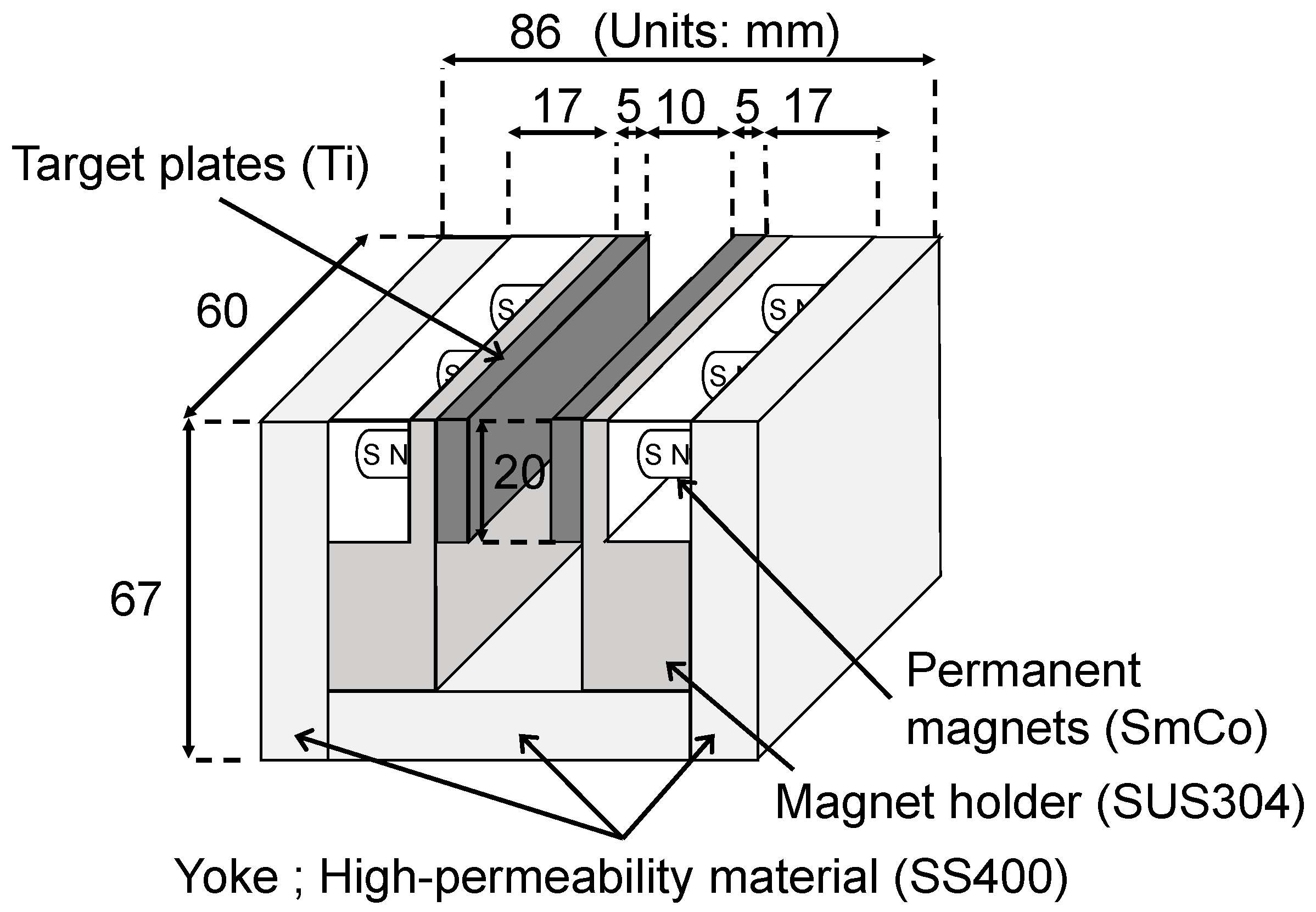
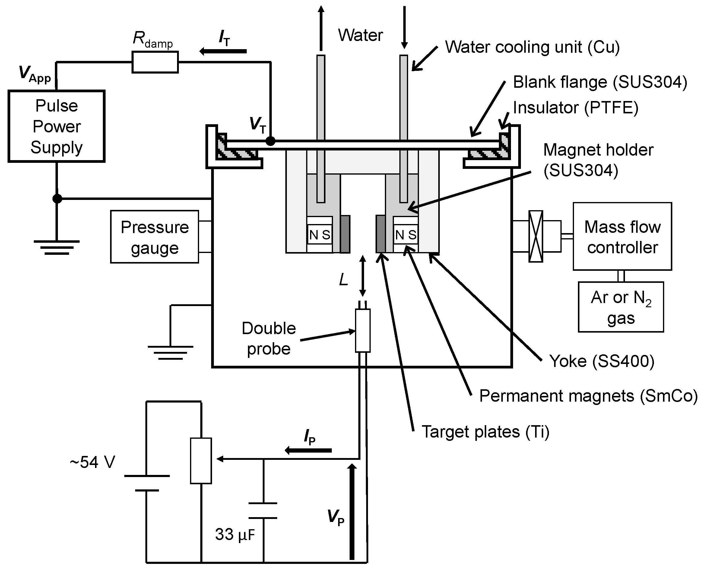
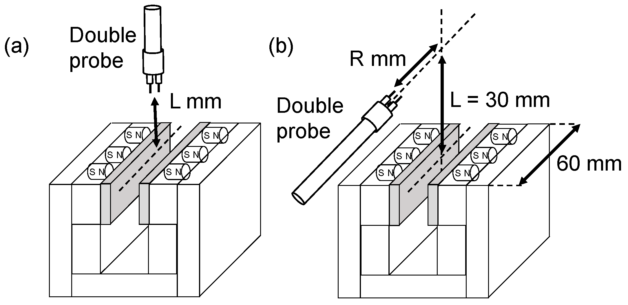
2. Experimental Setup and Procedure

Figure 1 shows a schematic diagram of the HPPS unit used in this experiment. The HPPS unit is compact in size. The dimensions of the unit are 60 mm in length, 67 mm in height, and 86 mm in width. A pair of titanium (Ti) plates has dimensions of 60 mm in length, 20 mm in height, and 5 mm in thickness and was used as the sputtering targets. The Ti target plates were placed on the magnet holders (SUS304). The samarium–cobalt (SmCo) permanent magnets (200 mT, 15 mm diameter, 10 mm height) were set behind each Ti plate. The gap between the facing Ti plates was set to be 10 mm. A magnetic field was produced perpendicular to the targets with a strength of approximately 70 mT.
Figure 2 shows a schematic of the experimental setup. A cylindrical vacuum chamber had dimensions of 320 mm diameter and 200 mm height. At first, the vacuum chamber was evacuated using a rotary pump, a mechanical booster pump, and a turbo molecular pump to gas pressure of 5 × 10⁻³ Pa. Following the evacuation process, the argon (Ar) or nitrogen (N2) gas was fed into the chamber through a mass flow controller (HORIBA, SEC-400MK3; Kyoto, Japan) to a gas pressure of 4 Pa. The pressure was observed with two different pressure gauges (MG-2I, M-320XG, Canon ANELVA Co., Kawasaki, Japan). The HPPS unit was mounted at the upper side of the chamber, rotating 180 degrees relative to the arrangement shown in Figure 1. The HPPS plasma was produced between the two target plates and diffused toward the lower direction of Figure 2. The 20 Ω resistor (Japan Resistor Mfg. Co., Ltd., GR400 100K, Nanto, Japan) was connected in series with the HPPS unit to prevent glow-to-arc transition. A rectangular pulse was employed to apply voltage Vapp with 600 µs in pulse width at −600 V to −1000 V in amplitude. The rectangular pulse voltage was applied to the HPPS unit through the dumping resistor using a high-voltage pulse power supply (PEKURUS, KJ06-3265; −3 kV, 100 A, 1 kHz, 1 ms, Kyoto, Japan). The pulse repetition rate was set to be 1 Hz. The target voltage VT was measured with a high-voltage probe (Tektronix, P5100A; 2.5 kV, 500 MHz, Tokyo, Japan). The target current IT was measured with current transformers (Peason, Current Monitor 411, Palo Alto, CA, USA). The voltage and current waveforms were monitored with a digital oscilloscope (Tektronix, DPO 4104B, Tokyo, Japan). The power consumed in the plasma P was obtained using VT and IT by the following equation:
P = V T × I T
The spatial distributions of electron temperature and ion density were obtained using the double probe measurements, as shown in Figure 3. The probe tip was a cylindrical tungsten electrode of 1 mm in diameter and 4 mm in exposed length. The rest of the probe was covered with a glass tube to protect it from exposure to plasma. The probe voltage varied from −40 V to 40 V. The potentials of the two electrodes of the double probe and the power supply that applied the voltage to the probe were floating, i.e., insulating from the grounded electrodes. A ceramic capacitor of 33 µF was connected in parallel to the probes to keep a voltage constant against the voltage drop by the probe current. The double probe was placed at the center between the target electrodes and at a distance L away from the HPPS unit to measure the vertical distribution of electron temperature and ion density. L = 0 mm was the position at the surface of the HPPS unit. In this measurement, L varied from 0 mm to 60 mm. In the case of measuring the horizontal distribution, the probe was also set to be a vertical distance L of 30 mm. The probe position of horizontal distance R changed from 0 mm to 80 mm in a parallel direction to the target plates. The probe current was measured for various probe voltages to obtain the V–I characteristics.
Figure 4a shows the typical waveform of the probe current at L = 0 mm as a function of probe bias. Each waveform is approximately symmetrical to the horizontal axis. The probe current increased with increasing probe bias and saturated at approximately 12 V. The probe current at a probe voltage of 0, ±4 V had a rise time delay due to the plasma discharge delay. Figure 4b shows the V–I characteristics of the double probe at L = 0 mm using probe current at the steady state of the waveforms. This curve was plotted using the current flowing in the probe at 400 µs as the steady state. Assuming that the electron energy distribution function is Maxwellian, the electron temperature Te is calculated as follows:
d ln Σ I i / I e 1 1 d V p = e k T e  
where e is the elementary charge, and k is the Boltzmann constant. ΣIi and Ie are the ion current and the electron current flowing in the probe at 400 µs, and Vp is the bias voltage of the probe. The ion density ni is calculated as follows:
n i = I i 1 0.61 e S e T e / m i
where Ii is the ion saturation current; S is the surface area of the probe, and mi is the ion mass.
The OES measurement was carried out using a spectrometer (Stellar-Net Inc., BLUE-Wave UVN-25; 600 Gr mm−1 grating, Tampa, FL, USA). The plasma emission was observed by focusing on the center of the gap using a condenser lens with a focal length of 200 mm, as shown in Figure 5. The exposure time was 1 s. The OES data were analyzed using a computer to estimate the excitation and ionization rates of the sputtered metal atoms and gas molecules using each line emission intensity.

3. Results

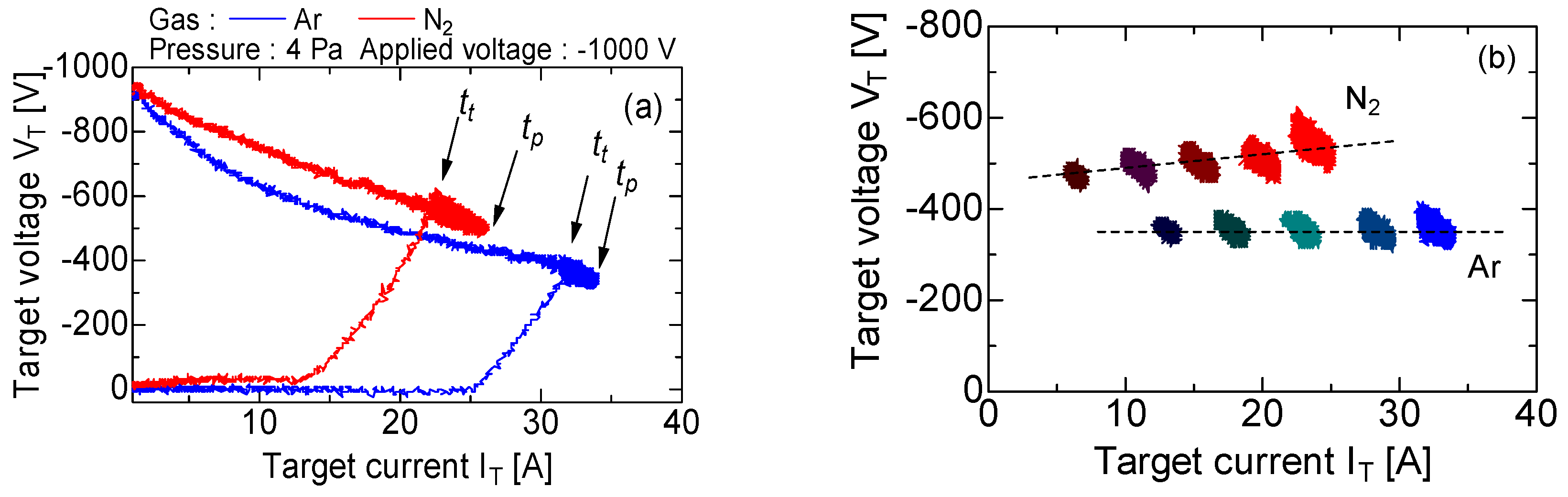
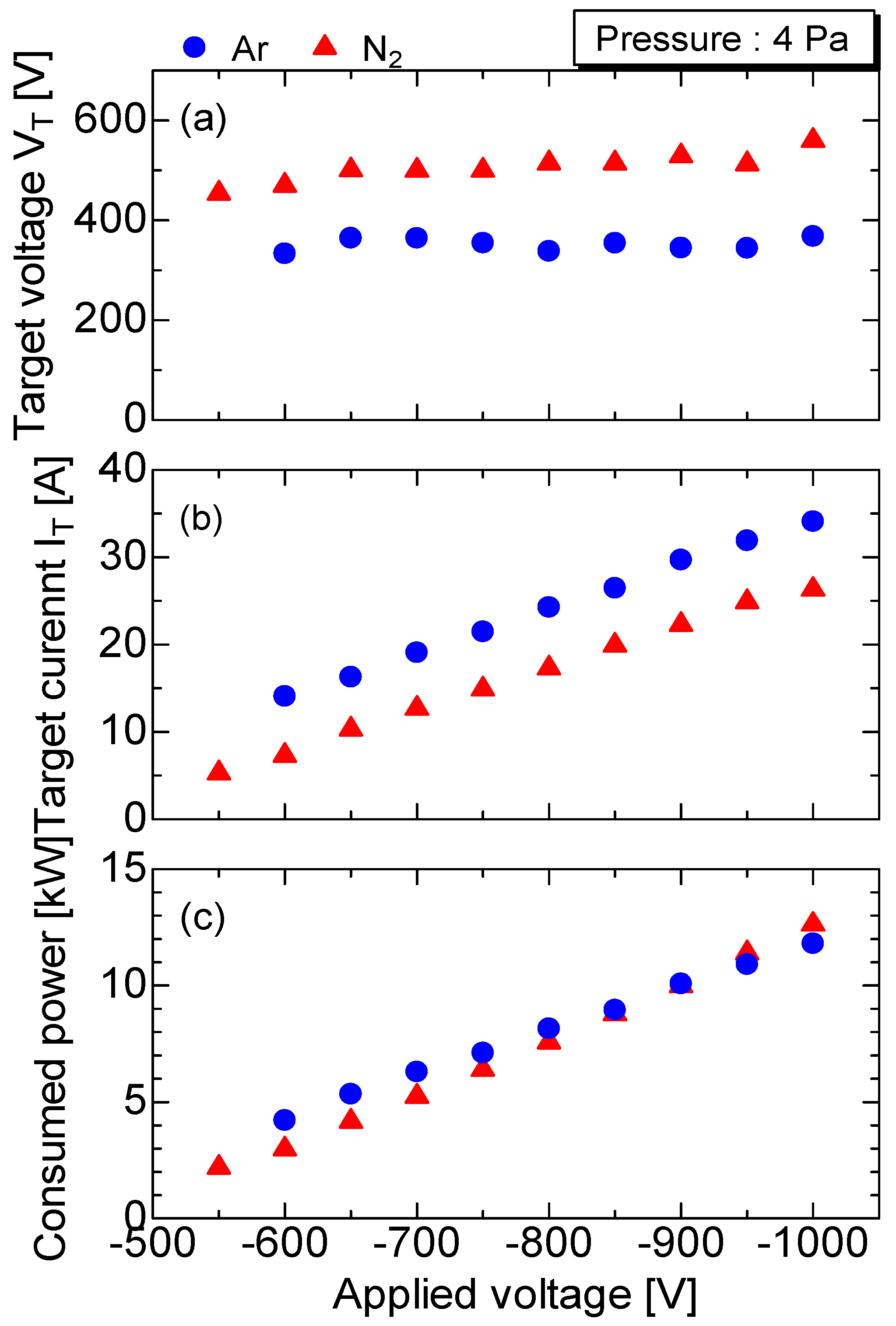
3.1. Electrical Characteristics of Glow Plasma

Figure 6 shows waveforms of the voltage applied to the target VT, the plasma current IT, and the power consumed in the plasma P (=VT × IT) in cases of nitrogen and argon used as working gases with the same gas pressure of 4 Pa. The initial target voltage is set to be −1000 V. The source voltage is maintained constant during a pulse width of 600 μs and is distributed to the plasma and the 20 Ω series connected resistor. The voltage waveforms include the surge voltage owing to the stray inductance of the plasma generation circuit when switching on. However, the target voltage shows the initial source voltage after a pulse voltage is applied to the target, as shown in Figure 6a,b, because plasma is not generated. The target voltage decreases from the initial voltage to a constant value determined by the plasma impedance. For the nitrogen HPPS plasma, the plasma current starts to increase at approximately 40 μs after applying voltage because of the plasma ignition. The plasma current increases to 26 A (shown as tp) with a rise time of 30 μs and then gradually decreases, followed by a stationary state of 23 A (shown as tt). At the stationary state, the consumed power and the plasma impedance are 12.5 kW and 24 Ω, which is obtained as a ratio of voltage and current as plasma impedance R = VT/IT (=560 V/23 A), respectively. For the argon case, the plasma ignition occurs at 190 μs after applying voltage. The plasma current increases to 33 A (shown as tp) with a time rise of 20 μs and then gradually decreases, followed by a stationary state of 32 A (shown as tt). The consumed power and the plasma impedance are 11.8 kW and 11 Ω (=360 V/32 A), respectively. The stationary currents of 23 and 33 A correspond to the current density of 0.96 (=23 A/24 cm2) and 1.38 A cm−2 at the target surface, respectively. The target voltage rapidly decreases from the initial voltage of −1000 V to the stational state of −500 V because of the voltage drop at the 20 Ω series resistor with the plasma current. The voltage of 500 V is higher than the typical value of nitrogen normal glow discharge [37]. This result indicates that the steady glow plasma is generated with a large current density of 0.96 A cm2. The power of 12.5 kW corresponds to the power density of 0.5 kW cm−2 (=12.5 kW/24 cm2) at the target.
Figure 7 shows the V−I characteristics obtained from the voltage and current waveforms, as shown in Figure 6. The delivered V–I characteristics of whole waveforms of the target voltage and the plasma current show a complicated shape because the waveforms consist of a stationary state (glow) phase and two transient phases: transient glow; and afterglow, as shown in Figure 7a [37]. The region between tp and tt indicates the steady-state glow characteristic and corresponds to between tp and tt in Figure 6. The two transient phases are indicated as transient glow (from IT = 0 to point tp) and afterglow (from point tt). Thus, we extracted only the stationary state phase from the V–I waveforms at various applied voltages [38]. As shown in Figure 7b, the plasma characteristics, the magnitude of the plasma current and the plasma sustaining voltage, are different for the nitrogen and the argon gas discharge. The argon plasma shows normal glow characteristics, with an almost constant plasma sustaining voltage of 350 V for the different discharge currents in a range from 12 to 34 A. However, the voltage of the nitrogen plasma increases from 480 to 550 V with the increasing current from 5 to 25 A. The cathode fall voltage of typical glow discharge without an external magnetic field is also determined by using source gas and cathode material. For example, the typical cathode fall voltages of normal glow discharge at the iron cathode are 215 and 165 V for the nitrogen and argon gases, respectively. The glow-sustaining voltage is mainly determined by the cathode fall voltage under the low gas pressure condition. The current density of a normal glow discharge is expressed as follows:
j ng p 2 = ε 0 l n 1 + γ γ 1 1 + γ 0 E c / p α p · v +   d E / p
where jng is the current density; ε 0 is the dielectric constant; γ is the secondary electron emission coefficient; E c / p is the reduced electric field in the vicinity of the cathode surface; α is the Townsend ionization coefficient; v + is the ion drift velocity, and E / p is the reduced electric field [50]. The α of argon is almost one-order higher than that of nitrogen, around 200 Td in a reduced electric field [51]. In other words, the higher applied voltage at nitrogen gas is more necessary than that at argon gas for the same Townsend coefficient value. Therefore, the difference in V–I characteristics between nitrogen and argon gas is almost consistent with the difference in the kinetic properties of the gases.

3.2. Power Deposition in Plasma

The power deposition into the glow plasma is an important factor in producing the high-density plasma. Figure 8 shows (a) the target electrode voltage at 600 μs, (b) the current through the target electrode at 600 μs, and (c) the power consumed in the plasma P (=VT × IT), respectively, as a function of the applied voltage for the nitrogen and argon gases at 4 Pa gas pressure. The target voltage is almost constant regardless of the applied voltage. The target voltage at 600 μs corresponds to the plasma sustaining voltage of the steady state (i.e., glow voltage). The target voltage of nitrogen gas is almost 500 V, which is larger than that of argon gas at 350 V, shown as the same tendency in Figure 7b. On the contrary, the target current of nitrogen gas is smaller than that of argon gas. The target current can be expressed using a circuit equation as follows:
I T = V a p p V T R 0
where Vapp is the applied voltage; VT is the target voltage, and R0 is the current damping resistor of 20 Ω, as shown in Figure 1. The target voltages VT are 500 V and 350 V for nitrogen and argon gases, respectively. Therefore, the difference in the target current between the nitrogen and argon gases is roughly estimated as 7.5 A as (500–350)/20. The estimated difference is almost in agreement with the measured values, as shown in Figure 8b. Moreover, the target currents increase with the increase in the applied voltage Vapp with the slope of 0.05 (=1/20), as estimated by Equation (5).
The consumed powers also linearly increase with increasing the applied voltage. After the applied voltage of −950 V, the consumed power of nitrogen gas is higher than that of argon gas. This phenomenon can also be explained by the equivalent circuit of the HPPS. The consumed power is expressed using the circuit equation as follows:
P = V T · I T = V a p p R 0 · I T · I T  
The Equation (6) can be transformed following the quadratic equation:
P = R 0 I T V a p p / 2 R 0 2 + V a p p 2 / 4 R 0
Figure 9 shows the consumed power P for nitrogen and argon gases as a function of the target current IT. The solid curves (1)–(5) indicate the estimation using Equation (7) for various applied voltages Vapp in the range from −600 V to −1000 V. The experimental results are also plotted for various applied voltages, as shown in Figure 7. Equation (7) indicates that the maximum value of the consumed power is Vapp2/80 at Vapp/40 of the target current IT by substituting 20 Ω into R0. For example, when the applied voltage is set at −600 V, the maximum consumed power is obtained at 6 kW at 15 A of the target current. This situation is close to the argon gas case because the target current is almost 15 A at −600 V of the applied voltage, as shown in Figure 8. Therefore, the consumed power, i.e., input power into the plasma of argon gas, is larger than that of nitrogen because the target current of nitrogen gas is 7.3 A at −600 A of the applied voltage. However, the calculated maximum consumed power increases to 10.1 kW at 22.5 A of the target current at −900 V of the applied voltage. This situation is close to the nitrogen gas case because the target current is 22 A at −900 V of the applied voltage. Therefore, the input power into the plasma of nitrogen gas is larger than that of argon gas. This analysis result indicates that the optimum condition for energy input into the plasma can be estimated using the equivalent circuit and plasma sustaining voltage for each gas shown in Figure 8a.

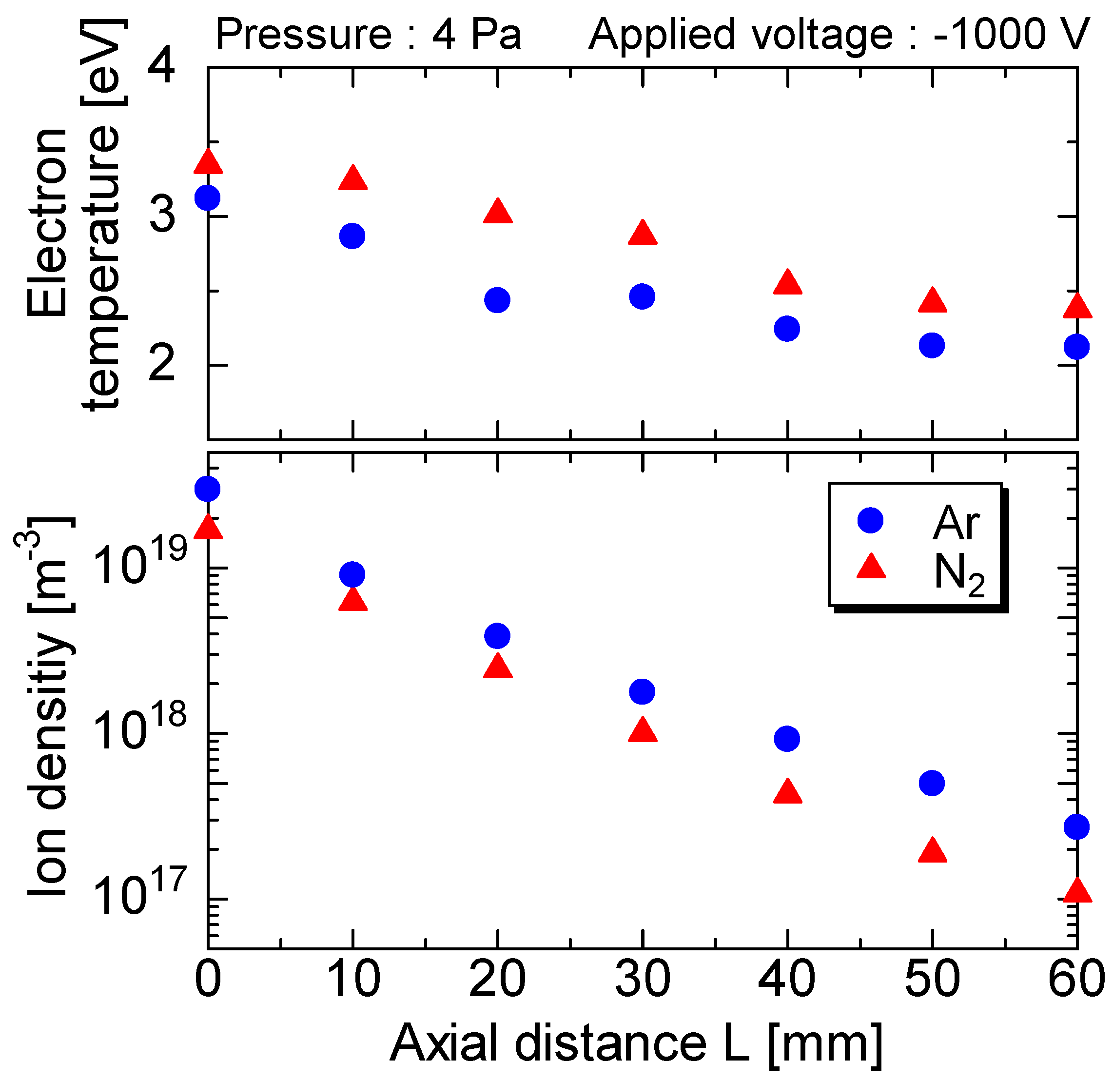
3.3. Ion Density and Electron Temperature of Plasma

The plasma parameters such as electron temperature and ion density are important information for the estimation of the plasma process performance. Figure 10 shows the axial profile of the electron temperature and the ion density of the glow plasma for two different gases, nitrogen and argon. The axial profile is defined as the vertical distance L from the electrode surface at the center of the horizontal position (R = 0), shown in Figure 3a. The electron temperature is in the range of 2.0 eV to 3.5 eV and is almost independent of gas species, nitrogen, and argon. Moreover, the value of 2.0–3.5 eV is almost equivalent to the previous report of the electron temperature 2–4 eV for pulse glow discharge [1,52]. The ion density at the surface of the electrode (L = 0), i.e., ionization region under the nitrogen gas condition, is 1.7 × 10¹⁹ m−3 and decreases with increasing the axial distance from the electrode surface, i.e., defuse region. The ion density of nitrogen gas at L = 60 mm is 1.0 × 10¹⁷ m−3, which is almost two orders lower than that at L = 0. In the argon gas case, the ion density is 3.0 × 10¹⁹ m−3 at L = 0 and decreases to 2.7 × 10¹⁷ m−3 with increasing the axial distance L from 0 to 60 mm. The difference in ion density in nitrogen and argon is considered from the reaction rate. Table 1 shows the rate coefficients for the primary ionization reaction of nitrogen and argon gases. The reaction rate vi is expressed using the following equation:
vi = K × ng × ne
where K is the reaction constant; ne is the electron density, and ng is the gas density obtained from pg/kTg using the gas pressure pg, Boltzmann constant k, and the gas temperature Tg. Since the plasma is electrically neutral, the electron number density is almost the same as the ion density (neni) in case the negatively charged ion is negligible. Using the electron temperature and ion density obtained by the double probe at L = 0, the reaction rates vi_N2 in nitrogen and vi_Ar in argon gases are calculated to be vi_N2 = 1.78 × 1024 m−3 s−1 and vi_Ar = 4.82 × 1024 m−3 s−1. The ratio of vi_N2 to vi_Ar results in vi_N2/vi_Ar = 1/2.7, indicating that argon is 2.7 times more ionized than nitrogen. Therefore, the ion density of nitrogen is estimated to be lower than that of argon gas.
Figure 11 shows the horizontal profile of the ion density of the glow plasma for the two different gases, nitrogen and argon. The horizontal profile is defined as the distance R from the center of the electrode at the vertical position L = 30 mm, shown in Figure 3b. The dotted line in the figure shows the edge of the HPPS unit. The ion density is almost independent of the horizontal position R between R = 0 to 30 mm, i.e., where the probe is located at the same distance from the ionization region. However, the ion density decreases from 9.1 × 10¹⁷ m−3 to 7.3 × 10¹⁶ m−3 with increasing the horizontal distance R from 30 to 80 mm under the nitrogen gas condition. In the case of argon, the ion density also decreases from 1.3 × 10¹⁸ m−3 to 1.6 × 10¹⁷ m−3 with increasing the horizontal distance R from 30 to 80 mm.

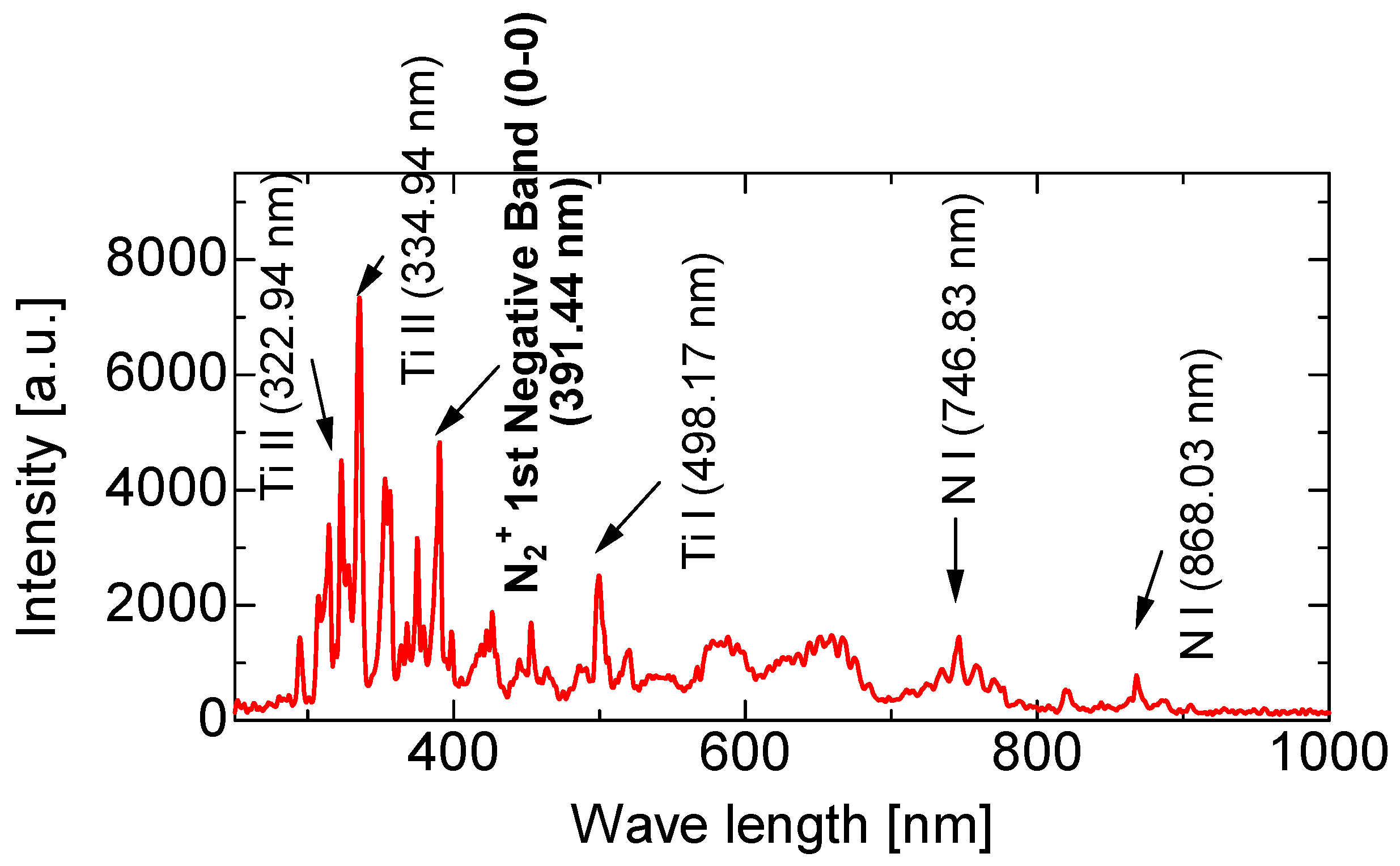
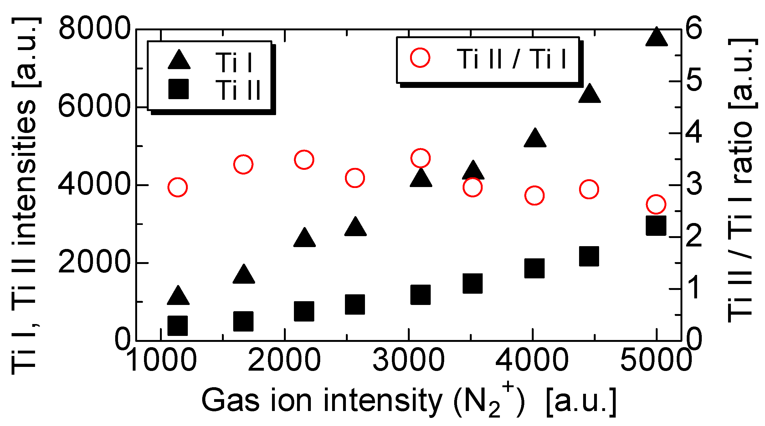
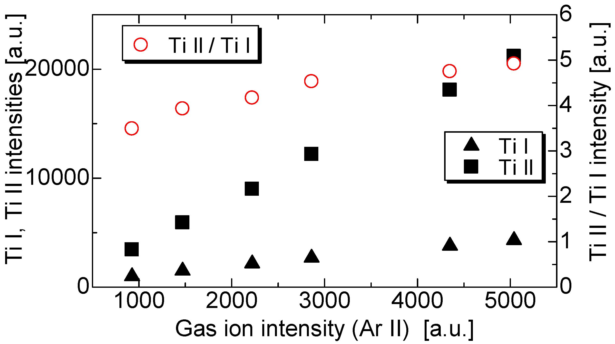
3.4. Spectroscopic Analysis

The optical measurement was carried out to evaluate the sputtering of the titanium target by the nitrogen ion. Figure 12 shows the emission spectrum from the glow plasma in the nitrogen gas. Many lines of light emission from the atomic nitrogen, the nitrogen ion (N2+ 1NB0-0; 391.44 nm), and the exited states of nitrogen molecules are confirmed, as shown in the figure. The light emission from the sputtered titanium neutral and ionized atoms, Ti I (498.17 nm) and Ti II (334.94 nm), are also confirmed in the same manner as the argon gas case reported in the reference [54]. This result indicates that the HPPS discharge promotes the sputtering of the titanium target and also the ionizing of the sputtered titanium atoms.
Figure 13 shows the intensities of the optical emission spectrum (OES) at 391.44, 498.17, and 334.94 nm corresponding excitation states of N2+, Ti I, and Ti II, respectively, as a function of power consumed by the plasma. The OES intensities of the gas ions and Ti increased with increasing consumed power. This result indicates that the HPPS discharge promotes the sputtering of the titanium target and also the ionizing of the sputtered titanium atoms. Figure 14 shows the OES intensities of 334.94 nm (Ti II) and 498.17 nm (Ti I) as a function of 391.44 nm (N2+). The intensity ratio of Ti II and Ti I is also plotted in the figure. The OES intensities of Ti II to Ti I increase with increasing OES intensity of N2+. On the other hand, the OES intensity ratio of Ti II to Ti I is not affected by the intensity of N2+. This result indicates that the increment of plasma density at the nitrogen gas mainly contributes to the increment of the sputtering rate through the increment of the ion flux from the nitrogen plasma into the titanium target.

4. Discussion

The HPPS plasma using nitrogen gas was produced to prepare titanium–nitrogen composited film. The titanium sputtering was confirmed through the OES measurement. The intensity of light emission of the sputtered titanium atoms (Ti I, Ti II) increased with the power consumed in the plasma (i.e., input power), as shown in Figure 13. The sputtering is generally caused by the ion flux from the plasma into the target material. The intensity of light emission of the gas ion (N2+) also increased with the consumed power, as shown in Figure 13. The input power from the pulse modulator into the HPPS plasma was expressed using the equivalent circuit Equation (7). The measured input powers were in good agreement with the calculation using Equation (7), as shown in Figure 9. Here, the optimum condition for power delivery from the power modulator to the HPPS for various working gases is discussed. The influence of working gas on the sputtering yield of the titanium target is also discussed for the preparation of the titanium-based composite film.
The maximum value of the input power from the power modulator into the plasma Pmax is expressed as Vapp2/4R0, where Vapp is the applied voltage, and R0 is the resistance of for current damping shown in Figure 1, at IT = Vapp/2R0, where IT is the target current, as shown by Equation (7). By inserting the condition into the Equation (5), the following equation is obtained:
I T = V a p p 2 R 0 = V a p p V T R 0
Equation (8) can be deformed to Vapp = 2VT, where VT is the target voltage (i.e., plasma sustaining voltage). The plasma sustaining voltage mainly consists of the cathode fall voltage Vcf and the bulk voltage Vbulk. The cathode fall voltage depends on the working gas and cathode material. The cathode fall voltage of the nitrogen is 1.3–1.8 times larger than that of novel gases such as argon, helium, and neon [50]. The cathode fall voltages of the negative gas (e.g., oxygen) and its gas mixture (e.g., air) are 1.3–1.7 times larger than that of the nitrogen [50,55]. Therefore, the optimum condition for the design of a power modulator for the HPPS plasma production is set to be around 1.0 kV of maximum output voltage for the nitrogen ( V T     500 V) and the argon ( V T     350 V) gases. However, the maximum voltage of the pulse modulator should be increased if the negative gas is used in the process.
The high-density nitrogen plasma of 1.7 × 10¹⁹ m−3 was successfully produced using the HPPS in the vicinity of the ionization region, as shown in Figure 10. The light emission from the sputtered Ti atoms was also confirmed, as shown in Figure 13. Moreover, the sputtering Ti atoms were ionized to Ti ions by the nitrogen plasma, as shown in Figure 14. Here, we discuss the sputtering performance and ionization efficiency of the nitrogen HPPS plasma in comparison with the argon HPPS plasma. Figure 15 shows the OES intensities of 334.94 nm (Ti II) and 498.17 nm (Ti I) as a function of 368.25 nm (Ar II). The intensity ratios of Ti II and Ti I are also plotted in a manner similar to Figure 14. The OES intensities of Ti I and Ti II increase with increasing OES intensity of argon ion, Ar II. The OES intensity ratios of Ti II to Ti I slightly increase with the intensity of Ar II. Moreover, The OES intensity ratio of Ti II to Ti I in the argon gas is in the range from 3.5 to 4.9, which is larger than that in nitrogen, in the range from 2.5 to 3.5 of the ratios. These results show that the argon ions effectively promote the sputtering and ionization of Ti in comparison to the nitrogen ion. In pulse sputtering, the number of sputtered atoms per pulse Nsput is expressed as follows:
N s p u t = Y s p u t · I T a v e · T p u l s e e
where Ysput is the effective sputter yield per ion; ITave is the averaged target current during the pulse application, and Tpulse is the pulse width of the applied voltage. Dividing both sides of this equation by the time gives the number of sputtered atoms per unit time. Assuming that Ysput is equal for both argon and nitrogen ions, to simplify the calculation, the difference in sputtering rate by gas species can be expressed by the ratio of the target currents IT. The ratio of the target currents IT_Ar of the argon gas and IT_N2 of the nitrogen gas can be obtained using Figure 8. The ratio IT_Ar/IT_N2 is obtained as almost 1.30 at the applied voltage of −1000 V. This result suggests that the sputtering per unit time is more effective at the argon gas as a working gas. Moreover, the ionization of the sputtered Ti atoms under the argon gas condition is also more effective than that at the nitrogen gas due to their high densities, as shown in Figure 10 and Figure 11.

5. Conclusions

The high-density nitrogen plasma was produced using a high-power pulsed power modulator to sputter titanium targets for the preparation of titanium nitride film. The high-power pulsed sputtering discharge was used to generate high-density glow plasma. The nitrogen glow plasma of HPPS was evaluated through the probe measurement and the spectroscopic analysis. The characteristics of the nitrogen glow plasma property were compared with that of the argon glow plasm to clarify the nitrogen glow plasma property. The glow plasma sustain voltage was almost constant (slightly increasing with the glow current) regardless of the applied voltage, showing normal glow characteristics. The ion density and electron temperature at the surface of the ionization region were obtained as 1.7 × 10¹⁹ m−3 and 3.4 eV, respectively, by the double probe measurements. The vertical distribution of ion density and electron temperature ranged from 1.1 × 10¹⁷ m−3 (at 6 cm from the target edge) to 1.7 × 10¹⁹ m−3 and from 2.4 eV (at 6 cm from the target edge) to 3.4 eV, respectively. From the emission spectra, the intensities of Ti II, Ti I, and N2+ increased with increasing input power. However, the intensities ratio of Ti II to Ti I was not affected by the intensities from N2+.

Author Contributions

T.S., S.I., K.T. (Katsuyuki Takahashi) and K.T. (Koichi Takaki) conceived and designed these experiments; T.S. and K.T. (Koichi Takaki) performed these experiments; T.S., S.I., K.T. (Katsuyuki Takahashi), S.M. and K.T. (Koichi Takaki) analyzed the data; T.S. and K.T. (Koichi Takaki) wrote this paper. All authors have read and agreed to the published version of the manuscript.

Funding

This research was supported by a Grant-in-Aid for Scientific Research (S) from the Japan Society for the Promotion of Science, Grant Number 19H05611.

Data Availability Statement

Data are contained within the article.

Acknowledgments

The authors would like to thank Ken Yukimura for his valuable comments and discussions. The authors would also like to thank Yutaka Shida at Iwate University for the technical support in preparing plasma chamber and double probes.

Conflicts of Interest

The authors declare no conflicts of interest.

References

  1. Helmersson, U.; Lattemann, M.; Bohlmark, J.; Ehiasarian, A.P.; Gudmundsson, J.T. Ionized physical vapor deposition (IPVD): A review of technology and applications. Thin Solid Films 2006, 513, 1–24. [Google Scholar] [CrossRef]
  2. Huang, N.; Yang, P.; Leng, Y.X.; Wang, J.; Sun, H.; Chen, J.Y.; Wan, J.Y. Surface modification of biomaterials by plasma immersion ion implantation. Surf. Coat. Technol. 2004, 186, 218–226. [Google Scholar] [CrossRef]
  3. Scheibe, H.J.; Schultrich, B. DLC film deposition by Laser-Arc and study of properties. Thin Solid Films 1994, 246, 92–102. [Google Scholar] [CrossRef]
  4. Chapin, J.S. The Planar Magnetron. Res. Dev. 1974, 25, 37–40. [Google Scholar]
  5. Thornton, J.A. Magnetron sputtering: Basic physics and application to cylindrical magnetrons. J. Vac. Sci. Technol. 1978, 15, 171–177. [Google Scholar] [CrossRef]
  6. Oks, E.M.; Savkin, K.P.; Yushkov, G.Y.; Nikolaev, A.G.; Anders, A.; Brown, I.G. Measurement of total ion current from vacuum arc plasma sources. Rev. Sci. Instrum. 2006, 77, 03B504. [Google Scholar] [CrossRef]
  7. Lehnert, B. Rotating Plasmas. Nuclear. Fusion. 1971, 11, 485–532. [Google Scholar] [CrossRef]
  8. Posadowski, W.M. Sustained self sputtering of different materials using dc magnetron. Vaccum 1995, 46, 1017–1020. [Google Scholar] [CrossRef]
  9. Kouznetsov, V.; Maca’k, K.; Schneider, J.M.; Helmersson, U.; Petrov, I. A novel pulsed magnetron sputter technique utilizing very high target power densities. Surf. Coat. Technol. 1999, 122, 290–293. [Google Scholar] [CrossRef]
  10. Gudmundsson, J.T.; Brenning, N.; Lundin, D.; Helmerssona, U. High power impulse magnetron sputtering discharge. J. Vac. Sci. Technol. A 2012, 30, 030801. [Google Scholar] [CrossRef]
  11. Anders, A.; Andersson, J.; Ehiasarian, A. High power impulse magnetron sputtering: Current-voltage-time characteristics indicate the onset of sustained self-sputtering. J. Appl. Phys. 2007, 102, 113303. [Google Scholar] [CrossRef]
  12. Yukimura, K.; Ogiso, H.; Nakano, S.; Nakao, S.; Takaki, K. Carbon Ion Production Using a High-Power Impulse Magnetron Sputtering Glow Plasma. IEEE Trans. Plasma Sci. 2013, 41, 3012–3020. [Google Scholar] [CrossRef]
  13. Konishi, T.; Yukimura, K.; Takaki, K. Fabrication of diamond-like carbon films using short-pulse HiPIMS. Surf. Coat. Technol. 2016, 286, 239–245. [Google Scholar] [CrossRef]
  14. Brauer, G.; Szyszka, B.; Vergohl, M.; Bandorf, R. Magnetron sputtering—Milestones of 30 years. Vacuum 2010, 84, 1354–1359. [Google Scholar] [CrossRef]
  15. Konishi, T.; Yukimura, K.; Takaki, K. Spatial Distribution of a High-Power Impulse Magnetron Sputtering Glow Plasma by a Controlled Unbalanced Magnetic Field. IEEE Trans. Plasma Sci. 2014, 42, 2786–2789. [Google Scholar] [CrossRef]
  16. Nakamura, K.; Yoshinaga, H.; Yukimura, K. Droplet-free high-density metal ion source for plasma immersion ion implantation. Nucl. Instr. Meth. Phys. Res. B 2006, 242, 315–317. [Google Scholar] [CrossRef]
  17. Yukimura, K.; Imai, T.; Takaki, K.; Ikehata, T. Hybrid Plasma Generation Triggered by a Shunting Arc Discharge Using a Positively Biased Electrode. IEEE Trans. Plasma Sci. 2007, 35, 1020–1026. [Google Scholar] [CrossRef]
  18. Takaki, K.; Ogiso, H.; Nakano, S.; Yukimura, K. A New Approach to High-Power Pulsed Glow Plasma Generation: Shunting Glow Plasma. IEEE Trans. Plasma Sci. 2012, 40, 1801–1808. [Google Scholar] [CrossRef]
  19. Yukimura, K.; Ehiasarian, A. Generation of RF plasma assisted high power pulsed sputtering glow discharge without using a magnetic field. Nucl. Instrum. Methods Phys. Res. Sect. B 2009, 267, 1701–1704. [Google Scholar]
  20. Saito, Y.; Shibata, K.; Takahashi, K.; Mukaigawa, S.; Takaki, K.; Yukimura, K. Global model analysis of Ar inductively coupled plasma driven by a 150 kHz-band high-power pulse burst. Jpn. J. Appl. Phys. 2019, 58, SAAB06. [Google Scholar] [CrossRef]
  21. Saito, Y.; Shibata, K.; Takahashi, K.; Mukaigawa, S.; Takaki, K.; Yukimura, K.; Ogiso, H.; Nakano, S. Silicon wafer etching by pulsed high-power inductively coupled Ar/CF4 plasma with 150 kHz band frequency. Jpn. J. Appl. Phys. 2020, 59, SHHE04. [Google Scholar] [CrossRef]
  22. Korolev, Y.D.; Frants, O.B.; Landl, N.V.; Shemyakin, I.A.; Geyman, V.G. High-Current Stages in a Low-Pressure Glow Discharge with Hollow Cathode. IEEE Trans. Plasma Sci. 2013, 41, 2087–2096. [Google Scholar] [CrossRef]
  23. Bardos, L.; Barankova, H.; Lebedev, Y.A. Performance of radio frequency hollow cathodes at low gas pressures. Surf. Coat. Technol. 2003, 163–164, 654–658. [Google Scholar] [CrossRef]
  24. Hirsch, E.H. On the mechanism of the Penning discharge. Br. Appl. Phys. 1964, 15, 1535–1543. [Google Scholar] [CrossRef]
  25. Knauer, W. Mechanism of the Penning Discharge at Low Pressures. J. Appl. Phys. 1962, 33, 2093–2099. [Google Scholar] [CrossRef]
  26. Bandorf, R.; Bräuer, G. Exotic Highly Ionized Pulse Plasma Processes. IOP Conf. Ser. Mater. Sci. Eng. 2012, 39, 012005. [Google Scholar] [CrossRef]
  27. Fridman, A.; Kennedy, L.A. 7.5.2 Penning Glow discharges. In Plasma Physics and Engineering; Taylor and Francis: New York, NY, USA, 2004; pp. 484–486. ISBN 1-56032-848-7. [Google Scholar]
  28. Hoshi, Y.; Naoe, M.; Yamanaka, S. High Rate Deposition of Iron Films by Sputtering from Two Facing Targets. Jpn. J. Appl. Phys. 1977, 16, 1715–1716. [Google Scholar] [CrossRef]
  29. Iljinas, A.; Dudonis, J.; Brucas, R.; Meškauskas, A. Thin Ferromagnetic Films Deposition by Facing Target Sputtering Method. Nonlinear Anal. Model. Control. 2005, 10, 57–64. [Google Scholar] [CrossRef]
  30. Yukimura, K.; Mieda, R.; Tamagaki, H.; Okimoto, T. Generation of droplet-free high-power pulsed sputtering (HPPS) glow plasma with several tens of kilowatts. Phys. Status Solidi (A) 2008, 205, 949–952. [Google Scholar] [CrossRef]
  31. Azuma, K.; Mieda, R.; Yukimura, K.; Tamagaki, H.; Okimoto, T. Electrical and Optical Characteristics of High-Power Pulsed Sputtering Glow Discharge. IEEE Trans. Plasma Sci. 2009, 37, 1178–1188. [Google Scholar] [CrossRef]
  32. Yukimura, K.; Mieda, R.; Tamagaki, H.; Okimoto, T. Electrical characteristics of arc-free high-power pulsed sputtering glow plasma. Surf. Coat. Technol. 2008, 202, 5246–5250. [Google Scholar] [CrossRef]
  33. Yukimura, K.; Ehiasarian, A.P.; Ogiso, H.; Nakano, S.; Azuma, K. Metal Ionization in a High-Power Pulsed Sputtering Penning Discharge. IEEE Trans. Plasma Sci. 2011, 39, 3125–3132. [Google Scholar] [CrossRef]
  34. Azuma, K.; Kimura, T. Plasma Parameters of Titanium-Based Metallic Plasma Generated by a Compact-Type High-Power Pulsed Sputtering Penning Discharge. IEEE Trans. Plasma Sci. 2016, 44, 3201–3206. [Google Scholar] [CrossRef]
  35. Kimura, T.; Mishima, T.; Azuma, K.; Nakano, S. Properties of diamond-like carbon films prepared by high power pulsed sputtering with two facing targets. Surf. Coat. Technol. 2016, 307, 1053–1058. [Google Scholar] [CrossRef]
  36. Kimura, T.; Yoshida, R.; Azuma, K.; Nakano, S. Preparation of titanium carbon nitride films by reactive high power pulsed sputtering Penning discharges. Vacuum 2018, 157, 192–201. [Google Scholar] [CrossRef]
  37. Takaki, K.; Taguchi, D.; Fujiwara, T. Voltage-current characteristics of high-current glow discharges. Appl. Phys. Lett. 2001, 78, 2646–2648. [Google Scholar] [CrossRef]
  38. Takaki, K.; Hosokawa, M.; Sasaki, T.; Mukaigawa, S.; Fujiwara, T. Production of atmospheric-pressure glow discharge in nitrogen using needle-array electrode. Appl. Phys. Lett. 2005, 86, 151501. [Google Scholar] [CrossRef]
  39. Tang, B.Y.; Chu, P.K.; Wang, S.Y.; Chow, K.W.; Wang, X.F. Methane and nitrogen plasma immersion ion implantation of titanium metal. Surf. Coat. Technol. 1998, 103–104, 248–251. [Google Scholar] [CrossRef]
  40. Czerwiec, T.; Renevier, N.; Michel, H. Low-temperature plasma-assisted nitriding. Surf. Coat. Technol. 2000, 131, 267–277. [Google Scholar] [CrossRef]
  41. Navinšek, B.; Panjan, P.; Krušič, J. Hard coatings on soft metallic substrates. Surf. Coat. Technol. 1998, 98, 809–815. [Google Scholar] [CrossRef]
  42. Santecchia, E.; Hamouda, A.M.S.; Musharavati, F.; Zalnezhad, E.; Cabibbo, M.; Spigarelli, S. Wear resistance investigation of titanium nitride-based coatings. Ceram. Int. 2015, 41, 10349–10379. [Google Scholar] [CrossRef]
  43. Datta, S.; Das, M.; Balla, V.K.; Bodhak, S.; Murugesan, V.K. Mechanical, wear, corrosion and biological properties of arc deposited titanium nitride coatings. Surf. Coat. Technol. 2018, 344, 214–222. [Google Scholar] [CrossRef]
  44. Kelly, P.J.; Arnell, R.D. Magnetron sputtering: A review of recent developments and applications. Vacuum 2000, 56, 159–172. [Google Scholar] [CrossRef]
  45. Liu, Z.Q.; Wang, W.J.; Wang, T.M.; Chao, S.; Zheng, S.K. Thermal stability of copper nitride films prepared by rf magnetron sputtering. Thin Solid Films 1998, 325, 55–59. [Google Scholar] [CrossRef]
  46. Jeyachandran, Y.L.; Narayandass, S.K.; Mangalaraj, D.; Areva, S.; Mielczarski, J.A. Properties of titanium nitride films prepared by direct current magnetron sputtering. Mater. Sci. Eng. A 2007, 445–446, 223–236. [Google Scholar] [CrossRef]
  47. Anders, A. Approaches to rid cathodic arc plasmas of macro- and nanoparticles: A review. Surf. Technol. 1999, 120/121, 319–330. [Google Scholar] [CrossRef]
  48. Benegra, M.; Lamas, D.G.; Fernández De Rapp, M.E.; Mingolo, N.; Kunrath, A.O.; Souza, R.M. Residual stresses in titanium nitride thin films deposited by direct current and pulsed direct current unbalanced magnetron sputtering. Thin Solid Films 2006, 494, 146–150. [Google Scholar] [CrossRef]
  49. Abe, S.; Takahashi, K.; Mukaigawa, S.; Takaki, K.; Yukimura, K. Comparison of plasma characteristics of high-power pulsed sputtering glow discharge and hollow-cathode discharge. Jpn. J. Appl. Phys. 2020, 60, 015501. [Google Scholar] [CrossRef]
  50. Korolev, Y.D.; Mesyate, G.A. Physics of Pulsed Breakdown in Gases; URO-Press: Moscow, Russia, 1998. [Google Scholar]
  51. Talviste, R.; Paris, P.; Raud, J.; Plank, T.; Erme, K. Experimental determination of the first Townsend ionization coefficient in mixtures of Ar and N2. J. Phys. D Appl. Phys. 2021, 54, 465201. [Google Scholar] [CrossRef]
  52. Sarakinos, K.; Alami, J.; Konstantinidis, S. High power pulsed magnetron sputtering: A review on scientific and engineering state of the art. Surf. Coat. Technol. 2010, 204, 1661–1684. [Google Scholar] [CrossRef]
  53. Kimura, T.; Kasugai, H. Experiments and global model of inductively coupled rf Ar/N2 discharges. J. Appl. Phys. 2010, 108, 033305. [Google Scholar] [CrossRef]
  54. Lieberman, M.A.; Lichtenberg, A.J. Principles of Plasma Discharges and Materials Processing, 2nd ed.; Wiley: New York, NY, USA, 2005. [Google Scholar]
  55. Sarakinos, K.; Alami, J.; Klever, C.; Wuttig, M. Growth of TiOX films by high power pulsed magnetron sputtering from a compound TiO1.8 target. Rev. Adv. Mater. Sci. 2007, 15, 44–48. [Google Scholar]
Figure 1. Schematic of the HPPS discharge unit.
Processes 12 01314 g001
Figure 2. Schematic of the experimental setup.
Processes 12 01314 g002
Figure 3. Measurement for spatial distribution of plasma as a function of (a) vertical distance L and (b) horizontal distance R.
Processes 12 01314 g003
Figure 4. Typical signals of the double-probe measurement; (a) probe current waveforms at L = 0 for various bias voltages, and (b) its V–I characteristics.
Processes 12 01314 g004
Figure 5. Schematic of the arrangement for optical measurement of the HPPS plasma.
Processes 12 01314 g005
Figure 6. Waveforms of the target voltage and the current for cases of (a) nitrogen and (b) argon gases at 4 Pa of gas pressure and −1000 V of the applied voltage. The temporal plasma consumed powers of the nitrogen and argon are shown in (c).
Processes 12 01314 g006
Figure 7. V–I characteristics obtained from the voltage and current waveforms in Figure 6. (a) the transient glow region; from IT = 0 (upper) to point of tp, steady state glow region; between points tp and tt, and afterglow region; from point tt to IT = 0 (lower). (b) steady-state glow voltage for two gases as a function of glow current. The glow current was controlled by the applied voltage in range from −600 V to −1000 V at 4 Pa gas pressure.
Processes 12 01314 g007
Figure 8. Electrical characteristics of the discharge for nitrogen and argon gas at 4 Pa of gas pressure for various applied voltages; (a) the target voltage; (b) the target current; and (c) the consumed power.
Processes 12 01314 g008
Figure 9. Consumed power for nitrogen and argon gases as function of target current at various applied voltages. The solid lines are estimated using circuit equations for various applied voltages. The triangle and circle plots are measured values for nitrogen and argon gases, respectively.
Processes 12 01314 g009
Figure 10. The electron temperature and ion density as a function of vertical distance L from the electrode surface at gas pressure of 4 Pa and −1000 V of applied voltage. The triangle and circle plots are measured values for nitrogen and argon gases, respectively.
Processes 12 01314 g010
Figure 11. The ion density as a function of of horizontal distance R from the electrode at axial distance of L = 30 mm, gas pressure of 4 Pa, and applied voltage of −1000 V. The triangle and circle plots are measured values for nitrogen and argon gases, respectively.
Processes 12 01314 g011
Figure 12. Spectrum of the light emission of the nitrogen plasma at 4 Pa of gas pressure and the −1000 V of the applied voltage.
Processes 12 01314 g012
Figure 13. Intensities of the optical emission spectrum at 391.44, 498.17, and 334.94 nm corresponding excitation states of N2+, Ti I, and Ti II, respectively, as a function of power consumed in the plasma at 4 Pa of gas pressure and the −1000 V of the applied voltage.
Processes 12 01314 g013
Figure 14. Intensities of the optical emission spectrum at Ti I (498.17 nm) and Ti II (334.94 nm) as a function of intensity of N2+ 391.44 nm, at 4 Pa gas pressure and the −1000 V applied voltage. The intensity ratio between Ti II and Ti I is also plotted as a function of N2+ intensity.
Processes 12 01314 g014
Figure 15. Intensities of the optical emission spectrum at Ti I (498.17 nm) and Ti II (334.94 nm) as a function of intensity of Ar II (368.25 nm) at 4 Pa gas pressure and the −1000 V applied voltage. The intensity ratio between Ti II and Ti I is also plotted as a function of Ar II intensity.
Processes 12 01314 g015
Table 1. Primary ionization reactions for nitrogen and argon gases.
ReactionRate Coefficient [m3 s−1]Ref.
N2 + e → N2+ + 2eKN2 = 2.8 × 10⁻¹⁴ exp (−18.56/Te)[53]
Ar + e → Ar+ + 2eKAr = 12.3 × 10⁻¹⁴ × Te0.59 exp (−17.44/Te)[54]
Disclaimer/Publisher’s Note: The statements, opinions and data contained in all publications are solely those of the individual author(s) and contributor(s) and not of MDPI and/or the editor(s). MDPI and/or the editor(s) disclaim responsibility for any injury to people or property resulting from any ideas, methods, instructions or products referred to in the content.

