Article

Substrate and Doping Effects on the Growth Aspects of Zinc Oxide Thin Films Developed on a GaN Substrate by the Sputtering Technique

by
R. Perumal
1,
Lakshmanan Saravanan
1 and
Jih-Hsin Liu
2,*
1
Department of Physics, Saveetha School of Engineering, Saveetha Institute of Medical and Technical Sciences, Chennai 602105, Tamil Nadu, India
2
Nanoscale Electronic Materials and Energy Technologies Lab, Department of Electrical Engineering, Tunghai University, Taichung 40704, Taiwan
*
Author to whom correspondence should be addressed.
Processes 2025, 13(4), 1257; https://doi.org/10.3390/pr13041257
Submission received: 13 March 2025 / Revised: 13 April 2025 / Accepted: 18 April 2025 / Published: 21 April 2025

Abstract

:
A one-micron-thick pure zinc oxide (ZnO) and nitrogen-doped zinc oxide (N-ZnO) film were fabricated on p-type, pristine (non-porous), and porous gallium nitride (GaN) substrates using a radio frequency (RF) sputtering technique at room temperature. The doping medium was nitrogen gas, which has a flow rate that ranges from 0 to 10 sccm (0 sccm refers to pure ZnO). The photoelectrochemical etching process, using ultraviolet light, was employed to etch the wafer surface and create a porous GaN substrate. ZnO films were developed on GaN with ZnO powder as the target material under vacuum conditions. This research aimed to investigate how variations in substrate and doping influenced the structural, optical, and electrical characteristics of the resulting thin films. The SEM images indicated that the pores developed on the etched GaN surface had a spherical shape. The A1 (LO) phonon peak at 750.2 cm−1 was observed in the Raman spectrum of the etched porous GaN. The X-ray diffraction (XRD) analysis confirmed that the films grown on GaN possessed a hexagonal wurtzite structure and the observed peak shift of (101) in all N-ZnO films suggested interstitial nitrogen doping. For the N-ZnO films, the UV-visible cut-off wavelength shifted towards the blue region. The root mean square (RMS) roughness of the N-ZnO films, measured using atomic force microscopy (AFM), was found to decrease with an increasing N-doping concentration. The 10 sccm sample exhibited the lowest roughness value of 1.1 nm, whereas the pure ZnO film showed the highest roughness of 3.4 nm. The N-ZnO thin films were found to exhibit p-type conductivity, as computed by Hall measurements using the van der Pauw method, and the higher value of carrier concentration obtained for the nitrogen gas flow rate of 8 sccm was 5.29 × 1021 cm−3.

1. Introduction

Zinc oxide (ZnO) thin films have garnered significant interest owing to their exceptional electrical, optical, and mechanical properties, which enable their versatile applications [1]. ZnO, with a wide bandgap of approximately 3.37 eV and a high exciton binding energy of around 60 meV, enables strong excitonic emission even at room temperature [2,3]. After doping, ZnO thin films demonstrate high transparency in the visible wavelength region, enhanced electrical conductivity, and strong piezoelectric characteristics. These properties make them ideal for optoelectronic devices, transparent conductive electrodes, sensors, and piezoelectric applications [4,5,6,7,8]. Several techniques, including sputtering, sol–gel processing, pulsed laser deposition, and chemical vapor deposition, are used to deposit ZnO films, each influencing their structural, morphological, and electrical properties. Moreover, ZnO is well known for its high optical transparency across the visible and near-infrared (NIR) spectral ranges, along with its excellent electrical conductivity, making it a highly suitable electrode material for optoelectronic device applications [9]. ZnO is commonly observed as an n-type semiconductor, a characteristic often attributed to native point defects such as oxygen vacancies and zinc interstitials. These intrinsic defects are believed to act as donor-like centers, contributing to the unintentional n-type conductivity in ZnO [10].
In general, ZnO-based optoelectronic devices are fabricated directly on Si substrates; however, achieving high internal quantum efficiency necessitates defect-free ZnO thin films. However, in practice, this is not feasible due to discrepancies in their crystal structures, which lead to differences in their thermal expansion coefficients [11,12]. The substrate significantly influences film growth by managing lattice and thermal mismatches, which induce stress in the deposited film. Moreover, the charge imbalance at the substrate–film interface can introduce defects during ZnO film growth, as the sudden interface creates an energetically unstable condition [13]. Therefore, the alternative findings are necessary and important to address this key issue regarding obtaining high-quality ZnO thin films. It is difficult to achieve high-purity epitaxial-grown ZnO films on an amorphous glass substrate, resulting in polycrystalline ZnO films with grain boundaries and defects. The lack of epitaxial alignment and the high defect density degrade the electrical properties of ZnO films [14]. The wurtzite-structure ZnO films are typically grown on (0001) Al2O3 substrates due to their structural similarity. However, there is a lattice mismatch of 30% between the basal planes of ZnO and Al2O3, along with an 18% mismatch between the smaller cell of Al atoms [15]. Özgür, Ü. et al. highlighted the challenges of growing ZnO films on silicon substrates, pointing out that the significant lattice mismatch between ZnO and Si—about 40%—results in the formation of defects in the ZnO film [16]. The defects and strain in ZnO films grown on Si can lead to poor optical quality, including reduced photoluminescence efficiency and increased defect-related emission [17]. It was reported that ZnO deposited on Si formed an amorphous interfacial layer of silicon oxide (SiO2) at the ZnO/Si interface. This oxide layer could act as a barrier against transporting the charge carriers and could reduce the electrical performance of devices [18]. Due to the chemical and structural differences between ZnO and Si, the adhesion of ZnO films to Si substrates can be poor, leading to the delamination or peeling of the film [19]. Growing ZnO thin films on silicon substrates can negatively impact the film quality due to structural incompatibilities. ZnO has a wurtzite crystal structure, whereas Si possesses a diamond cubic structure, resulting in a lattice mismatch that can introduce strain and defects in the ZnO film. The thermal expansion coefficients between ZnO and Si can cause thermal stress during thin film deposition [20,21], which may negatively affect the optical properties of the ZnO films. GaN substrate is considered for the growth of ZnO thin films, since the lattice mismatch between GaN and ZnO is relatively small [22]. Dong et al. combined zinc oxide (ZnO) and gallium nitride (GaN) layers to fabricate heterostructured LED devices for the production of cost-effective solid-state lighting devices [23]. Both ZnO and GaN have a wurtzite crystal structure, which promotes epitaxial growth and reduces the formation of grain boundaries and defects [24], and this also enhances the photoluminescence efficiency and hinders defect-related emissions. When GaN epitaxial layers are grown on porous GaN templates, which exhibit a significantly higher surface-to-volume ratio compared to bulk GaN, they show reduced strain and lower dislocation densities, making them beneficial for efficient light harvesting applications [25]. Thin films grown on porous substrates are found to have a greater relaxation of mismatch strain and have effectively reduced defect density through the lateral dislocation bending mechanism [26]. GaN substrates have high thermal stability, allowing for the high-temperature growth and processing of ZnO films without significant degradation in quality [27]. ZnO films grown on GaN substrates have enhanced piezoelectric properties due to the high-quality epitaxial growth, making them suitable for piezoelectric devices and sensors [28], and reducing the inherent substrate-induced stress and dislocations associated with growth while depositing ZnO on a porous template.
Nitrogen (N) doping in ZnO has been widely investigated to tailor its electrical and optical properties, with a particular focus on achieving p-type conductivity. Since intrinsic ZnO typically unveils n-type conductivity due to native defects like oxygen vacancies and zinc interstitials, the incorporation of nitrogen, a group-V element, aims to introduce acceptor states and compensate for the dominant donor defects. Nitrogen substitutes oxygen in the ZnO lattice, acting as an acceptor that can introduce hole carriers that facilitate hole conduction [29]. Nitrogen doping can shift the photoluminescence (PL) emission peak of ZnO to the visible region, enhancing yellow–green emission due to the formation of nitrogen-related defect states. Enhanced photocatalytic performance, especially under exposure to visible light, has been observed in ZnO doped with nitrogen. The introduction of nitrogen creates localized states within the bandgap, reducing the energy required for photoexcitation and enhancing the material’s ability to drive photochemical reactions, such as water splitting for hydrogen production [30].
Recently, doped ZnO nanomaterials and thin films have been fabricated using different techniques to increase the structural properties, optical transmittance, and electrical conductivity for optoelectronic device applications [29,31,32,33]. Among the various physical deposition techniques, magnetron sputtering is the most suitable for growing high-quality n-type doped ZnO thin films, as it allows for precise control over the doping concentration while achieving a high deposition rate.
In this work, ZnO films were deposited on non-porous (unetched) and porous (etched) GaN substrates using the radio frequency (RF) magnetron sputtering technique at 300 K. The purification and etching process were performed on the GaN substrate using the photoelectrochemical etching method to produce porous GaN. The pure and nitrogen-doped ZnO (N-ZnO) thin films were later deposited on the etched porous GaN substrate. Our aim was to achieve p-type ZnO thin films grown on the non-porous and porous GaN substrates by doping with nitrogen. We aimed to enhance the electrical conductivity and carrier concentration of the N-doped film by varying the nitrogen gas flow rate. The Hall measurements were performed to investigate the electrical properties, employing the van der Pauw method. The effect of substrates and nitrogen doping on the morphological, structural, electrical and optical properties of the grown ZnO films were analyzed and the obtained results were discussed in detail.

2. Experimental Techniques

2.1. Preparation of Porous GaN Substrate

In these experiments, an etched porous GaN wafer (PGaN) was utilized as one of the substrates along with non-porous (pristine) GaN to grow pure ZnO and N-ZnO films. The commercial unintentionally doped n-type 2-inch diameter of a GaN wafer (from Technologies and Devices International Inc., Silver Spring, MD, USA) was used in this experiment as a substrate for the growth of a ZnO film. A GaN wafer with a thickness of approximately 3.0 μm and a carrier concentration of around 4.38 × 1017 cm−3 was used. The entire process was carried out in two distinct phases. In the first phase, a surface-etched PGaN was prepared by the photo electrochemical etching method. The custom-made Teflon cell contained a sulfuric acid (H2SO4) and hydrogen peroxide (H2O2) mixture in a 3:1 v/v ratio. Platinum wire and GaN substrates acted as the cathode and the anode, respectively. The porous GaN was made at a constant current density of 10 mA/cm2 by illumining with a UV lamp with 500 W power for 60 min to develop adequate deep-level pores. The etched GaN wafer was thoroughly rinsed with deionized (DI) water and dried using high-purity nitrogen gas before the deposition process [34].

2.2. Preparation of Pure and N-Doped ZnO Films on GaN Substrate

The deposition of ZnO films was the second phase of the experiment. The HHV A500 radio frequency (RF) sputtering system was employed to deposit ZnO films on the GaN substrate. A high-purity (99.999%) zinc oxide (ZnO) target was used. The sputtering power was maintained at 150 W, with high-purity argon used as the sputtering gas to purge the chamber, raising the pressure from a base level of 3 × 10⁻⁵ mbar to 2 × 10⁻² mbar. For N-ZnO films, the nitrogen gas flow rate was varied between 0 and 10 sccm in steps of 2 sccm (sccm denotes cubic centimeter per minute) through a mass flow controller. One-micron-thick ZnO films were deposited onto both non-porous and porous gallium nitride (GaN) substrates. The grown pure and N-doped ZnO films on both of the substrates were then annealed at 500 °C under a nitrogen atmosphere for one hour. The deposition process is presented in Table 1.

2.3. Characterization Techniques

Field emission scanning electron microscopy (FESEM, model FEI/NovaNanoSEM450, FEI Ltd., Eindhoven, the Netherlands) was employed to examine the surface morphology of pristine and porous gallium nitride and the deposited ZnO films. The morphology and roughness of the grown films were investigated through an atomic force microscope (AFM, Model: Dimension Edge, Bruker, MA, USA). The crystalline structure and the film growth orientation were analyzed by X-ray diffraction (XRD) (PAN analytical X’Pert PROMRDPW3040, Almelo, the Netherlands) with CuKα radiation (λ = 0.154 nm). The transmittance spectra of the GaN substrate and the deposited ZnO films were examined using a UV-visible spectrophotometer (Jobin Yvon HR 800UV, Edison, NJ, USA). A He–Cd laser (325 nm) and an argon ion laser (514.5 nm) were used, respectively, as excitation sources to obtain photoluminescence (PL) and Raman spectral data. The electrical properties of the pure and N-ZnO films, including electrical resistivity, carrier concentration, and electron mobility, were measured using a Hall effect system (Lakeshore Controller 601/DRC-93CA, Westerville, OH, USA).

3. Results and Discussion

3.1. Structural and Optical Analysis of GaN Substrates

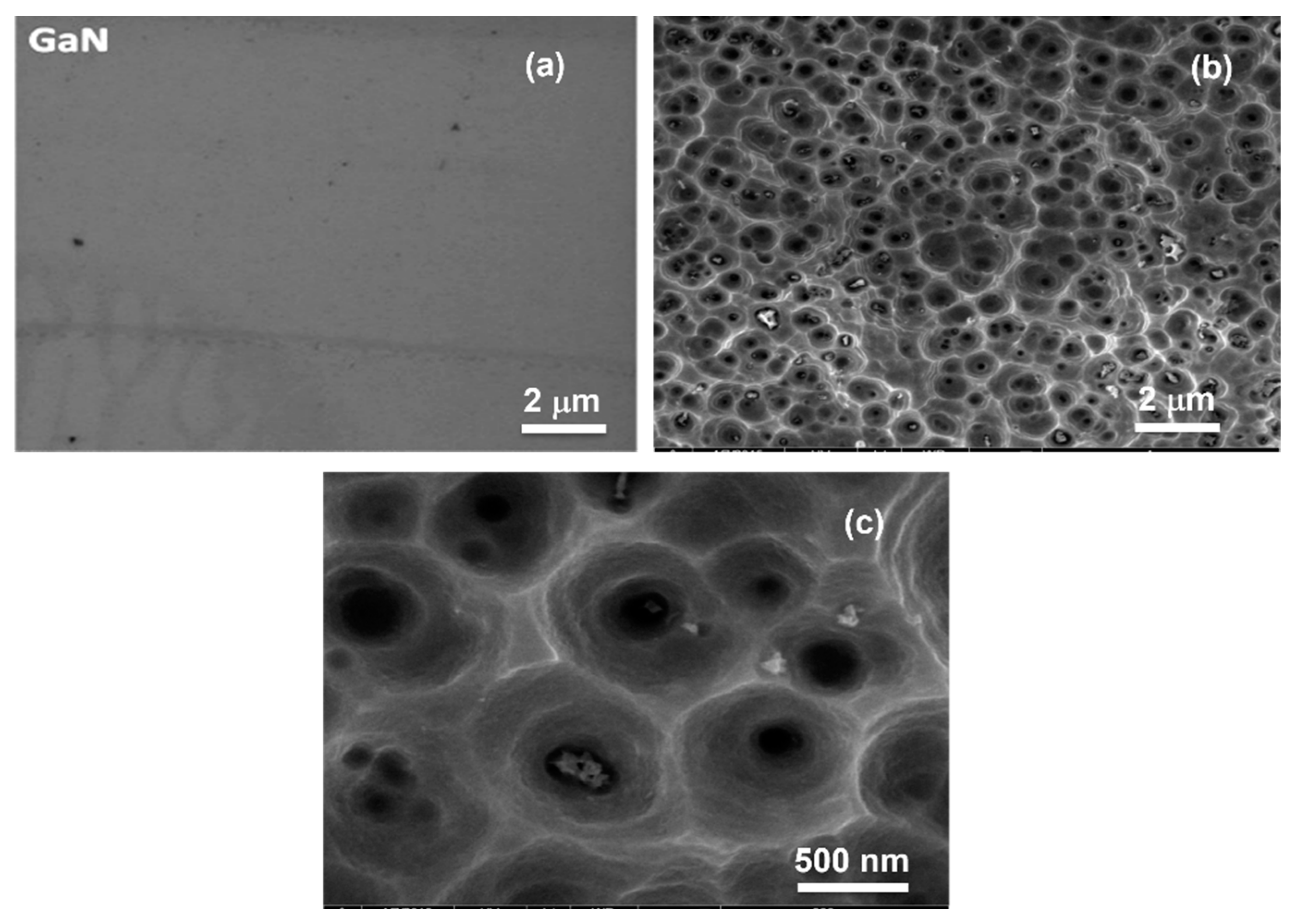
3.1.1. SEM Analysis of Pristine and Porous GaN Substrates

The photoelectrochemical etching process was adapted to modify the surface of the GaN substrate. The porous nanostructure was developed on the flat GaN substrate surface (shown in Figure 1a) due to the energy band bending downward by the application of the bias that depleted electrons from the substrate material [35]. In this course of action, holes were accumulated that oxidized the substrate surface by the injection of electrons. As the etchant subsequently dissolved the produced oxides, the substrate surface transformed into a porous structure, further enhanced by UV light illumination. The etched GaN surfaces are shown in Figure 1b,c with an enlarged image. The SEM image of the porous GaN surface showed that most of the developed pores were spherical in shape [36]. The formation of spherical pores in an etched GaN substrate is predicted to reduce light scattering and enhance light extraction efficiency. The FESEM micrographs revealed a uniform distribution of spherical pores across the etched GaN wafer, with most exhibiting nanopore sizes, except for a few star-, elongated-, triangular-, and square-shaped pores. This observation highlighted the effective etching capability of the electroless etching technique at producing spherical pores on the GaN wafer. The resulting micrographs demonstrated a remarkable porous network, devoid of any ridge-like structures.

3.1.2. Raman Spectral Analysis of Pristine and Porous GaN Substrates

Raman spectral analysis is conducted at room temperature to investigate the phonon modes present, as shown in Figure 2. As can be seen, two such modes, E2 (TO) and A1 (LO), are observed in the Raman spectra for the non-porous and porous gallium nitride substrates [37]. The obtained Raman peaks are located at 532 cm−1 for the A1 (TO) phonon, 568.2 cm−1 for the E2 (high) phonon, and at 740 cm−1 for the A1 (LO) phonon modes, respectively. Here, we observe the A1 (LO) phonon peak at 750.2 cm−1 for the etched porous GaN. The surface nanostructure improves the quality of the porous GaN substrate, enhances Raman scattering efficiency, and facilitates stronger interactions. It also delivers higher Raman intensity compared to an unetched GaN substrate due to the relaxation in the substrate-induced stress and also due to having less mismatch dislocations with a higher surface area. Moreover, all these modes exhibit a red shift to having higher frequencies compared to the unetched pristine GaN substrate. This shift is due to the release of compressive stress in the porous GaN, influenced by the quantum confinement effect of the porous structures [38]. However, the observed Raman shift is slightly lower, indicating minimal stress from defects. This confirms that the etched porous GaN wafer in this study is nearly stress-free and is suitable for ZnO film deposition [39]. The improvement of the substrate quality might be attributed to the disordering of the crystalline structure.

3.2. Structural, Morphological, and Electrical Properties of ZnO Films

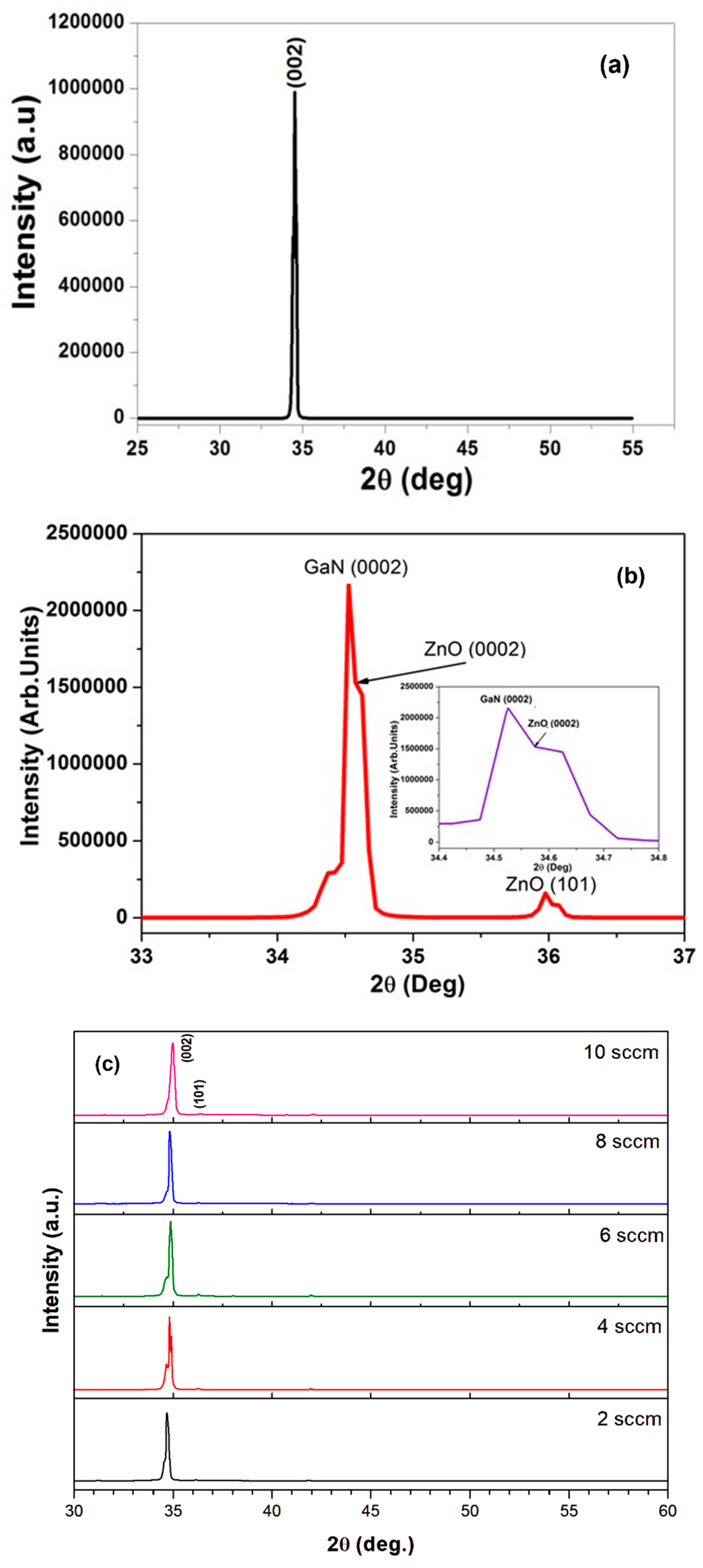
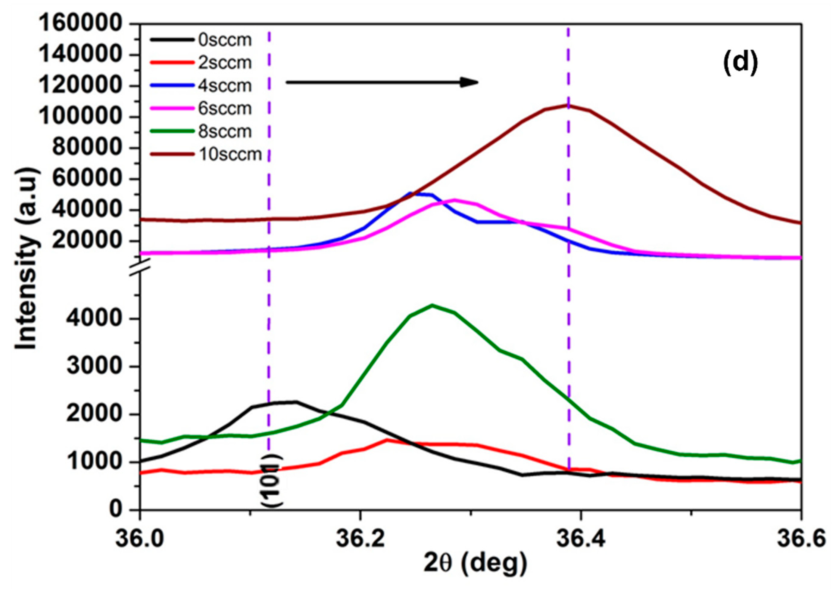
3.2.1. XRD Analysis of Pure and N-ZnO on Porous GaN Substrate

To evaluate the crystalline nature of the grown ZnO films, X-ray diffraction (XRD) analysis was performed, and the resulting diffraction curves are presented in Figure 3a–c. Figure 3a,b illustrate the pure zinc oxide film grown on non-porous and porous GaN substrates, respectively. These diffraction peaks indicate that the deposited films have a hexagonal wurtzite phase, verified with standard data card No. 00-005-0664 [40]. Figure 3c presents the XRD data for the N-ZnO films deposited on the porous GaN substrate. It was confirmed that higher quality ZnO films were grown on the porous GaN substrate than the non-porous substrate by the narrow and high intense diffraction peak of ZnO with the same crystal orientation of GaN. It was observed that the grown epitaxial film on both substrates was oriented along the (002) crystal plane at 2θ = 34°. All the ZnO films were found to be grown preferentially along the c-axis. As shown in Figure 3b, the epitaxial ZnO film grown on a porous substrate exhibits an additional low-intensity peak at 36.36°, corresponding to the ZnO (101) plane. The diffraction peaks of the porous GaN substrate also exhibited a high intensity in the same crystal orientation as ZnO. The presence of high-intensity diffraction peaks ensured that the excellent crystal quality of ZnO films on porous GaN was due to the stress-free and reduced defects compared to a film grown on a non-porous substrate. Nitrogen doping could have also reduced the crystallite size, accompanied by peak broadening in the XRD pattern [41].
It is well known that dopant ions tend to occupy substitutional sites rather than interstitial, due to the lower energy barrier associated with nitrogen incorporation [42]. The diffraction data did not reveal any additional nitrogen-related diffraction peaks, indicating that nitrogen was incorporated solely into the ZnO lattice. This confirmed the absence of any secondary nitrogen compounds or complexes [43]. The ionic radius of O2− was 1.40 Å, just below that of N3− (1.46 Å). This smaller difference in ionic radii could have led to lattice distortion or strain when nitrogen was doped into ZnO, and it was expected that nitrogen would prefer to substitute O atoms in the crystal lattice of ZnO. When N3− replaced O2− in the ZnO lattice during doping, it acted as an acceptor, compensating for oxygen vacancies and reducing both defect density and the concentration of conduction electrons. The low-intensity (101) peak of ZnO films was studied by magnifying the peak for pure and N-ZnO samples, as shown in Figure 3d, to confirm the substitution of nitrogen in the ZnO lattice. It was observed that the (101) diffraction peak shifted toward a higher angle, accompanied by noticeable peak broadening compared to the pure ZnO film. The peak shift observed in all N-doped films compared to undoped ZnO indicated interstitial nitrogen doping, leading to lattice contraction due to internal strain [44,45,46]. Increased peak broadening suggested a smaller crystallite size or lattice defects caused by nitrogen incorporation affecting the electronic and optical properties of ZnO films.

3.2.2. SEM Analysis of Pure and Nitrogen-Doped ZnO on GaN

The SEM micrographs of the grown pure ZnO films on both non-porous and porous substrates are shown in Figure 4a,b, respectively. Additionally, the nitrogen-doped ZnO film deposited on porous GaN substrate is presented in Figure 4c. From the images, it is evidenced that all the grown pure and nitrogen-doped ZnO films were attached well to the GaN substrate. Compared to the ZnO film on a non-porous substrate, the film deposited on the porous substrate exhibited labyrinth patterns due to the release of air during the annealing process. This resulted in a growth pattern where several ZnO nanoparticles clustered together, forming an agglomerated structure [47]. It was attributed to the fact that the spherical pores in the GaN substrate were filled with ZnO particles and due to having a matrix with GaN which effectively modified the substrate’s nature by releasing the stress present in the substrate. This predominately improved the film quality by minimizing the dislocations of the grown films compared to non-porous substrate films. The filling of ZnO nanoparticles into the spherical pores of GaN was simplified, improving the adhesion of the grown ZnO film to the porous GaN substrate. This favored the smooth and compact morphology of grown ZnO films.

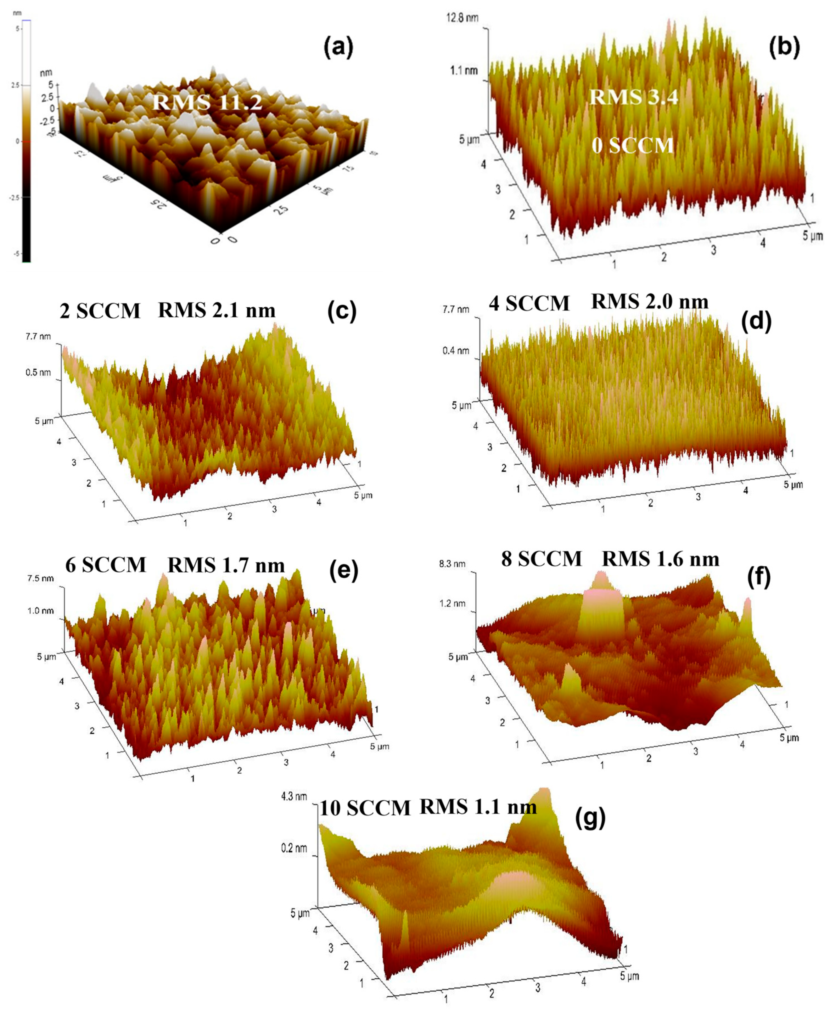
3.2.3. Atomic Force Microscopic Analysis of Pure ZnO and N-ZnO Films

Figure 5 shows the AFM topographical images of the pure ZnO and nitrogen-doped ZnO (N-ZnO) films deposited on gallium nitride (GaN) substrates. The AFM images were captured by scanning a 5 µm × 5 µm area of the sample surface, as shown in Figure 5a,b, respectively, for the pure ZnO film deposited on non-porous and porous GaN substrate. Figure 5c–g represent the N-ZnO film deposited on porous GaN substrate, respectively. The AFM images show that the grown metal oxide films on porous GaN have a smooth and compact morphology which highly favors solar cell device performance [48]. The surface was composed of high-density homogenous grains for each film sample, and we observed that the grain size decreased gradually towards the higher nitrogen content in the ZnO film. As seen in 3D AFM images of the surface, grain growth was found to be dense with highly homogenous distribution with smaller RMS values upon doping [49]. The root mean square (RMS) values of the ZnO films on non-porous and porous GaN substrates were tabulated in Table 2. It was clear that the RMS (roughness) value obtained from the AFM images for the films deposited on porous GaN decreased compared to films grown on an unetched (non-porous) substrate. The obtained RMS value for the pure ZnO film grown on a non-porous GaN was 11.2 nm, while the same value was decreased to 3.4 nm when the film was grown on a porous GaN substrate. This confirmed that the porous structure of GaN favored smoothing the ZnO film surface during the particle deposition over the substrate. This smoothing behavior greatly enhanced the diffusion ability of the atoms, leading to a significant decrease in surface roughness. Consequently, the film quality was improved compared to the ZnO film grown on a non-porous substrate. For the N-ZnO film sample with a gas flow rate of 10 sccm, a low roughness value of 1.1 nm was observed on the porous GaN substrate.

3.2.4. Photoluminescence Analysis of ZnO Films on GaN Substrates

The photoluminescence spectra of the ZnO films grown on both pristine and porous GaN substrates are shown in Figure 6. Two distinct emission peaks were observed in both films, namely near band edge (NBE) emission and the deep-level (DLE) emission in the visible region, respectively. The NBE emission peak at 375 nm and the low-intensity broader DLE emission peak were observed for both samples. However, the obtained peak for the film grown on the porous substrate is significantly narrower with increasing intensity compared to the film grown on the non-porous GaN substrate. The notable enhancement in luminescence efficiency was attributed to the suppression of substrate-induced stress and growth-related dislocations in ZnO films grown on GaN, which illustrated that the film grown on the porous GaN substrate exhibited high optical properties. The electron concentration involved in the photoluminescence process significantly increased due to the higher surface-to-volume ratio of the porous structure. Porosity plays a dominant role in enhancing emission intensity, resulting from the higher concentration of emitted photons in porous GaN. Furthermore, it was noted that the low-intensity, broader DLE peak shifted towards the red region for the ZnO film on porous GaN, compared to the green region for the ZnO film grown on the non-porous GaN substrate. Porous substrates typically exhibit reduced stiffness relative to dense substrates, leading to lower film strain during deposition. The decreased strain mitigates the formation of structural defects, such as dislocations and vacancies, thereby minimizing non-radiative recombination pathways and enhancing photoluminescence (PL) efficiency [50,51].

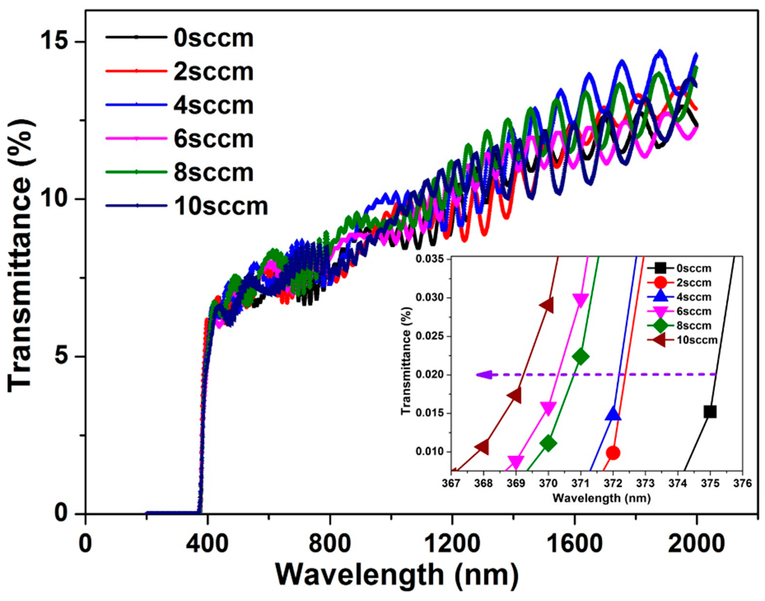
3.2.5. UV-Visible Spectra of ZnO Films on GaN Template

The optical properties of both undoped and N-ZnO films on the GaN template were investigated using UV-visible optical transmittance spectroscopy. The spectra were recorded over a wavelength range of 300 to 2000 nm and are presented in Figure 7. The obtained transmission spectra exhibit interference oscillations, which result from the film thickness and the difference in the refractive index between the film and the substrate. In the nitrogen-doped ZnO films, the cut-off wavelength is blue-shifted by 8 nm (i.e., from 374 nm to 367 nm) for different gas flow rates. It is also considered that the band gap widening in ZnO film is due to the effect of nitrogen doping in the lattice. Doping the ZnO film with nitrogen atoms shifts the Fermi level below the valence band by increasing the hole concentration, which leads to a widening of the band gap in the grown films [52]. The magnified UV-Vis transmittance spectra in the inset of Figure 7 clearly show a blue shift in the N-ZnO film samples with increasing nitrogen doping content, supporting our previous findings [34].

3.2.6. Electrical Properties of ZnO Films on GaN Substrate

The Hall measurements were executed to examine the electrical properties, including the carrier mobility, carrier concentration, and electrical resistivity, for pure ZnO films and nitrogen-doped ZnO films (N-ZnO). We employed the van der Pauw method [53,54] for calculating the values of the pure and doped ZnO films and the obtained results are plotted in Figure 8. From the plot, we found that all the pure ZnO and N-doped ZnO films exhibited p-type conductivity due to the acceptor level incorporation in the ZnO lattice by the inclusion of dopant nitrogen [55]. The nitrogen-doped ZnO sample with 6 sccm nitrogen gas flow rate was found to have slightly higher resistivity than other doped samples. This decrement in conductivity at higher doping levels, causing nitrogen to form complexes such as N2 molecules or creating N-O defects, reduced conductivity or led to semi-insulating behavior in ZnO films [56]. The electrical resistivity for N-ZnO films was significantly reduced to the order of 10−3 Ω·cm, in contrast to the pure ZnO sample, which exhibited a resistivity of 1.095 Ω·cm. This decrement in the resistivity of N-ZnO films increased the hole concentration from 4.71 × 10¹⁷ to 5.29 × 1021 cm−3. The obtained hole concentration values measured from the Hall measurements for the deposited films were 2.12 × 10¹⁸, 8.54 × 10¹⁹, 4.40 × 10²¹, 5.29 × 10²¹, and 7.99 × 1018 cm−3, for the nitrogen flow rates of 2, 4, 6, 8, and 10 sccm, respectively. The N-ZnO sample with an 8 sccm nitrogen gas flow rate was found to have a higher carrier concentration of 5.29 × 1021 cm−3. The pinning of the Fermi level was responsible for the decreased hole concentration observed at higher nitrogen doping levels [57]. In addition to the pinning of the Fermi level, the doped thin films demonstrated the successful incorporation of nitrogen into the ZnO film. This incorporation led to the formation of p-type ZnO, as nitrogen substituted oxygen at specific lattice (interstitial) positions. This nitrogen acted as a p-type acceptor in the fabricated ZnO thin films. The optimal nitrogen incorporation was achieved at an N2 flow rate of 8 sccm, resulting in an increased carrier concentration. However, further increases in the flow rate led to a decline in nitrogen doping concentration, attributed to the ionization of the N2 gas. This process may have generated reactive nitrogen species that promoted the formation of compensating defects, thereby reducing the effectiveness of nitrogen doping [58].
The carrier mobility of the N-doped ZnO films was found to follow a zigzag pattern. The intensified ionized impurity scattering in the ZnO lattice, caused by the increased nitrogen content, effectively reduced the carrier mobility. The sample with optimized nitrogen content was likely to provide sufficient hole concentration, thereby minimizing grain boundary scattering compared to the other doped samples. The N-ZnO film with a 4 sccm nitrogen gas flow rate delivered a higher mobility than other film samples. In contrast to the sample with a nitrogen flow rate of 10 sccm, the carrier mobility was found to be increasing again. The decrease in mobility with the increase in nitrogen doping was consistent with increased scattering from defects and impurities which caused by nitrogen-doping-induced defects created by the presence of N2, or N-O complexes, which acted as scattering centers [59].

4. Conclusions

A porous structure was formed on the pristine GaN surface, followed by the deposition of pure zinc oxide (ZnO) nanoparticles. N-ZnO thin films were also grown on non-porous GaN substrates to study the influence of the substrate and nitrogen doping on the quality of the as-grown ZnO films. The ultraviolet-light-assisted photoelectrochemical etching technique was adapted to develop the porous nanostructure over the surface of the pristine GaN substrate. The physical evaporation coating technique and radio frequency magnetron sputtering method were used to deposit the metal oxide films over both porous and non-porous GaN substrates at room temperature. The FESEM micrographs of the GaN surface that were obtained revealed the development of spherical-shaped pores with an excellent porous network throughout the surface of the substrate, without any elevated patterns. The filling of ZnO nanoparticles in the pores of GaN resulted in the strong adhesion of the grown ZnO film to the porous GaN substrate. This led to the formation of intricate patterns, in contrast to the deposition of particles on the non-porous substrate. The XRD pattern revealed that the grown ZnO film over the porous substrate established better diffraction intensity towards the (002) crystalline orientation. The shift of the (101) diffraction peak toward a higher angle, observed in all N-ZnO films, indicated interstitial nitrogen doping, which induced internal strain in the lattice due to lattice contraction. In the UV-Vis transmittance spectra, the increasing nitrogen doping level in the ZnO films caused the cut-off wavelength to shift towards the blue region by 8 nm, i.e., from 374 to 367 nm, which could be ascribed to the widening of the band gap. A low roughness value of 1.1 nm was observed for the N-ZnO film on the porous GaN substrate at a nitrogen gas flow rate of 10 sccm, as determined from AFM topography. The emission properties of the N-doped films were sufficiently improved through the nanostructuring process, which was further ascertained with the enhancement of luminescence intensity. The red shift observed in the Raman spectral data indicated the relaxation of compressive stress in the porous GaN substrate. Hall measurements confirmed that all the nitrogen-doped ZnO films demonstrated p-type properties with better electrical conductivity. A substantial reduction in the electrical resistivity of the N-ZnO film was achieved, reaching the order of 10−3 Ω·cm. A higher value of carrier concentration was obtained for the optimal nitrogen gas flow rate of 8 sccm, which was 5.29 × 1021 cm−3. The ZnO film doped with nitrogen at a flow rate of 8 sccm was observed to exhibit a higher carrier concentration.

Author Contributions

Investigation, Methodology, and Writing—original draft, R.P.; Manuscript writing—review and editing, L.S.; Funding acquisition, J.-H.L. All authors have read and agreed to the published version of the manuscript.

Funding

This research was funded by Tunghai University and the National Science and Technology Council, Taiwan, R.O.C., grant number NSTC 112-2622-E-029-007.

Data Availability Statement

The data presented in this study are available on request from the corresponding author.

Conflicts of Interest

The authors declare that they have no conflicts of interest.

References

  1. Nagaraj, G.; Mohammed, M.K.; Shekargoftar, M.; Sasikumar, P.; Sakthivel, P.; Ravi, G.; Dehghanipour, M.; Akin, S.; Shalan, A.E. High-performance perovskite solar cells using the graphene quantum dot–modified SnO2/ZnO photoelectrode. Mater. Today Energy 2021, 22, 100853. [Google Scholar] [CrossRef]
  2. Khiari, M.; Gilliot, M.; Lejeune, M.; Lazar, F.; Hadjadj, A. Preparation of Very Thin Zinc Oxide Films by Liquid Deposition Process: Review of Key Processing Parameters. Coatings 2022, 12, 65. [Google Scholar] [CrossRef]
  3. Mo, G.; Cui, Y.; Yin, J.; Gao, P. Influence of ZnO Film Deposition Parameters on Piezoelectric Properties and Film-to-Substrate Adhesion on a GH4169 Superalloy Steel Substrate. Micromachines 2022, 13, 639. [Google Scholar] [CrossRef] [PubMed]
  4. Tian, Z.R.; Voigt, J.A.; Liu, J.; Mckenzie, B.; Mcdermott, M.J.; Rodriguez, M.A.; Konishi, H.; Xu, H. Complex and Oriented ZnO Nanostructures. Nat. Mater. 2003, 2, 821–826. [Google Scholar] [CrossRef] [PubMed]
  5. Rekha, S.M.; Neelamana, H.V.; Bhat, S.V. Recent Advances in Solution-Processed Zinc Oxide Thin Films for Ultraviolet Photodetectors. ACS Appl. Electron. Mater. 2023, 5, 4051–4066. [Google Scholar] [CrossRef]
  6. Shinde, S.S.; Shinde, P.S.; Bhosale, C.H.; Rajpure, K.Y. Optoelectronic properties of sprayed transparent and conducting indium doped zinc oxide thin films. J. Phys. D Appl. Phys. 2008, 41, 105109. [Google Scholar] [CrossRef]
  7. Ponja, S.D.; Sathasivam, S.; Parkin, I.P.; Carmalt, C.J. Highly conductive and transparent gallium doped zinc oxide thin films via chemical vapor deposition. Sci. Rep. 2020, 10, 638. [Google Scholar] [CrossRef]
  8. Franco, M.A.; Conti, P.P.; Andre, R.S.; Correa, D.S. A review on chemiresistive ZnO gas sensors. Sens. Actuators Rep. 2022, 4, 100100. [Google Scholar] [CrossRef]
  9. Chen, Z.; Wang, J.; Wu, H.; Yang, J.; Wang, Y.; Zhang, J.; Bao, Q.; Wang, M.; Ma, Z.; Tress, W.; et al. A Transparent Electrode Based on Solution-Processed ZnO for Organic Optoelectronic Devices. Nat. Commun. 2022, 13, 4387. [Google Scholar] [CrossRef]
  10. Liu, L.; Mei, Z.; Tang, A.; Azarov, A.; Kuznetsov, A.; Xue, Q.-K.; Du, X. Oxygen vacancies: The origin of n-type conductivity in ZnO. Phys. Rev. B 2016, 93, 235305. [Google Scholar] [CrossRef]
  11. Klingshirn, C. ZnO: Material, physics, and applications. ChemPhysChem 2007, 8, 782–803. [Google Scholar] [CrossRef] [PubMed]
  12. Wang, Z.; Wang, F.; Wang, L.; Jia, Y.; Sun, Q. First-principles study of negative thermal expansion in zinc oxide. J. Appl. Phys. 2013, 114, 063508. [Google Scholar] [CrossRef]
  13. Wang, L.; Liu, Y.C.; Xu, C.S.; Qiu, Y.Q.; Zhao, L.; Rong, X.M. Effect of nitrogenized Si (111) substrates on the quality of ZnO films grown by pulsed laser deposition. J. Phys. D Appl. Phys. 2009, 42, 035307. [Google Scholar] [CrossRef]
  14. Fortunato, E.; Barquinha, P.M.C.; Pimentel, A.C.M.B.G.; Gonçalves, A.M.F.; Marques, A.J.S.; Martins, R.F.P.; Pereira, L.M.N. Wide-bandgap high-mobility ZnO thin-film transistors produced at room temperature. Appl. Phys. Lett. 2004, 85, 2541–2543. [Google Scholar] [CrossRef]
  15. Chen, Y.; Ko, H.J.; Hong, S.K.; Yao, T. Layer-by-layer growth of ZnO epilayer on Al2O3(0001) by using a MgO buffer layer. Appl. Phys. Lett. 2000, 76, 559. [Google Scholar] [CrossRef]
  16. Özgür, Ü.; Alivov, Y.I.; Liu, C.; Teke, A.; Reshchikov, M.A.; Doğan, S.; Avrutin, V.; Cho, S.-J.; Morkoç, H. A comprehensive review of ZnO materials and devices. J. Appl. Phys. 2005, 98, 041301. [Google Scholar] [CrossRef]
  17. Vanheusden, K.; Warren, W.L.; Seager, C.H.; Tallant, D.R.; Voigt, J.A.; Gnade, B.E. Mechanisms behind green photoluminescence in ZnO phosphor powders. J. Appl. Phys. 1996, 79, 7983–7990. [Google Scholar] [CrossRef]
  18. Vasanthi, V.; Sivanantham, N.; Saathvika, L.; Gopalakrishnan, N. Metal oxide charge transport materials for light emitting diodes—An overview. Mat. Sci. Semicond. Process. 2023, 165, 107679. [Google Scholar] [CrossRef]
  19. Wang, Z.L. Zinc oxide nanostructures: Growth, properties, and applications. J. Phys. Condens. Matter 2004, 16, R829–R858. [Google Scholar] [CrossRef]
  20. Hanada, T. Basic Properties of ZnO, GaN, and Related Materials. In Oxide and Nitride Semiconductors. Advances in Materials Research; Yao, T., Hong, S.K., Eds.; Springer: Berlin/Heidelberg, Germany, 2009; Volume 12. [Google Scholar]
  21. Chao, C.H.; Wei, D.H. Synthesis and characterization of high c-axis ZnO thin film by plasma enhanced chemical vapor deposition system and its UV photodetector application. J. Vis. Exp. 2015, 3, 53097. [Google Scholar] [CrossRef]
  22. Hamdani, F.; Yeadon, M.; Smith, D.J.; Tang, H.; Kim, W.; Salvador, A.; Botchkarev, A.E.; Gibsor, J.M.; Polyakov, A.Y.; Skowronski, M.; et al. Microstructure and optical properties of epitaxial GaN on ZnO (0001) grown by reactive molecular beam epitaxy. J. Appl. Phys. 1998, 83, 983–990. [Google Scholar] [CrossRef]
  23. Dong, J.J.; Zhang, X.W.; Yin, Z.G.; Wang, J.X.; Zhang, S.G.; Liu, X. Ultraviolet electroluminescence from ordered ZnO nanorod array/p-GaN light emitting diodes. Appl. Phys. Lett. 2012, 100, 171109. [Google Scholar] [CrossRef]
  24. Look, D.C. Recent advances in ZnO materials and devices. Mater. Sci. Eng. B 2001, 80, 383–387. [Google Scholar] [CrossRef]
  25. Inoki, C.K.; Kuan, T.S.; Lee, C.D.; Sagar, A.; Feenstra, R.M.; Koleske, D.D.; Adesida, I. Growth of GaN on porous SiC and GaN substrates. J. Electron. Mater. 2003, 32, 855–860. [Google Scholar] [CrossRef]
  26. Gangopadhyay, A.; Maros, A.; Faleev, N.; Smith, D.J. Strain relaxation in low-mismatched GaAs/GaAs1-xSbx/GaAs heterostructures. Acta Mater. 2019, 162, 103–115. [Google Scholar] [CrossRef]
  27. Norton, D.P.; Heo, Y.W.; Ivill, M.P.; Ip, K.; Pearton, S.J.; Chisholm, M.F.; Steiner, T. ZnO: Growth, doping, and processing. Mater. Today 2004, 7, 34–40. [Google Scholar] [CrossRef]
  28. Wang, Z.L. Nanopiezotronics. Adv. Mater. 2007, 19, 889–892. [Google Scholar] [CrossRef]
  29. Shafiqul, I.M.; Deep, R.; Lin, J.; Yoshida, T.; Fujita, Y. The Role of nitrogen dopants in ZnO nanoparticle-based light emitting diodes. Nanomaterials 2022, 12, 358. [Google Scholar] [CrossRef]
  30. Cerrato, E.; Privitera, A.; Chiesa, M.; Salvadori, E.; Paganini, M.C. Nitrogen-doped Zinc oxide for photo-driven molecular hydrogen production. Int. J. Mol. Sci. 2022, 23, 5222. [Google Scholar] [CrossRef]
  31. Musiliyu, K.A.; Ogunmola, E.D.; Ajayi, A.A.; Abodunrin, O.W. Effect of concentration on the properties of nitrogen-doped zinc oxide thin films grown by electrodeposition. Mater. Renew. Sustain. Energy 2023, 12, 23–29. [Google Scholar] [CrossRef]
  32. Wang, X.; Xin, S.; Tao, B.; Huang, B.; Subramaniam, V.; Ramachandran, K.; Zhang, F.; Shang, S.; Liu, X. Study of the Preparation and Performance of Mg-Doped Si/Al2O3/ZnO Nanowall Heterojunction UV Detector. ACS Appl. Nano Mater. 2024, 7, 21401–21409. [Google Scholar] [CrossRef]
  33. Gopalakrishnan, R.; Ashokkumar, M. Comparative assessment of transition metals doping effects on structural, optical, optical conductivity, and photocatalytic features of ZnO nanoparticles. J. Mater. Sci. Mater. Electron. 2024, 35, 1614. [Google Scholar] [CrossRef]
  34. Perumal, R.; Hassan, Z. Effect of nitrogen doping on structural, morphological, optical and electrical properties of radio frequency magnetron sputtered zinc oxide thin films. Phys. B Condens. Matter 2016, 490, 16–20. [Google Scholar] [CrossRef]
  35. Seo, J.W.; Oh, C.S.; Cheong, H.S.; Yang, J.W.; Youn, C.J.; Lim, K.Y. UV-assisted electrochemical oxidation of GaN. J. Korean Phys. Soc. 2002, 41, 1017–1020. [Google Scholar]
  36. Yam, F.K.; Hassan, Z.; Ng, S.S. Porous GaN prepared by UV assisted electrochemical etching. Thin Solid Film. 2007, 515, 3469–3474. [Google Scholar] [CrossRef]
  37. Davydov, V.Y.; Kitaev, Y.E.; Goncharuk, I.; Smirnov, A.; Graul, J.; Semchinova, O.; Uffmann, D.; Smirnov, M.; Mirgorodsky, A.; Evarestov, R. Phonon dispersion and Raman scattering in hexagonal GaN and AlN. Phys. Rev. B 1998, 58, 12899. [Google Scholar] [CrossRef]
  38. Al-Heuseen, K.; Hashim, M.R.; Ali, N.K. Effect of different electrolytes on porous GaN using photo-electrochemical etching. Appl. Surf. Sci. 2011, 257, 6197–6201. [Google Scholar] [CrossRef]
  39. Zeng, Y.; Ning, J.; Zhang, J.; Jia, Y.; Yan, C.; Wang, B.; Wang, D. Raman analysis of E2 (High) and A1 (LO) phonon to the stress-free GaN grown on sputtered AlN/Graphene buffer layer. Appl. Sci. 2020, 10, 8814. [Google Scholar] [CrossRef]
  40. Abed, C.; Bouzidi, C.; Elhouichet, H.; Gelloz, B.; Ferid, M. Mg doping induced high structural quality of sol–gel ZnO nanocrystals: Application in photocatalysis. Appl. Surf. Sci. 2015, 349, 855–863. [Google Scholar] [CrossRef]
  41. Ibrahim, K.M.; Saleh, W.R.; Al-Sammarraie, A.M.A. Structural and optical properties of ZnO nanostructures synthesized by hydrothermal method at different conditions. Nano Hybrids Compos. 2022, 35, 75–83. [Google Scholar] [CrossRef]
  42. Ahmed, F.; Kumar, S.; Arshi, N.; Anwar, M.S.; Koo, B.H. Morphological evolution between nanorods to nanosheets and room temperature ferromagnetism of Fe-doped ZnO nanostructures. Cryst. Eng. Comm. 2012, 14, 4016–4026. [Google Scholar] [CrossRef]
  43. Tu, M.-L.; Su, Y.-K.; Ma, C.-Y. Nitrogen-doped p-type ZnO films prepared from nitrogen gas radio-frequency magnetron sputtering. J. Appl. Phys. 2006, 100, 053705–053708. [Google Scholar] [CrossRef]
  44. Zhang, X.; Qin, J.; Xue, Y.; Yu, P.; Zhang, B.; Wang, L.; Liu, R. Effect of aspect ratio and surface defects on the photocatalytic activity of ZnO nanorods. Sci. Rep. 2014, 4, 4596. [Google Scholar] [CrossRef] [PubMed]
  45. Siva, N.; Sakthi, D.; Ragupathy, S.; Arun, V.; Kannadasan, N. Synthesis, structural, optical and photocatalytic behavior of Sn doped ZnO nanoparticles. Mater. Sci. Eng. B 2020, 253, 114497. [Google Scholar] [CrossRef]
  46. Hirai, M.; Kumar, A. Infrared Lattice Vibrations of Nitrogen-doped ZnO Thin Films. Mater. Res. Soc. Symp. Proc. 2007, 1035, 707. [Google Scholar] [CrossRef]
  47. Decremps, F.; Datchi, F.; Saitta, A.M.; Polian, A.; Pascarelli, S.; Di Cicco, A.; Baudelet, F. Local structure of condensed zinc oxide. Phys. Rev. B 2003, 68, 104101. [Google Scholar] [CrossRef]
  48. Kang, J.H.; Song, A.; Park, Y.J.; Seo, J.H.; Walker, B.; Chung, K.-B. Tungsten-doped zinc oxide and indium–zinc oxide films as high-performance electron-transport layers in N–I–P perovskite solar cells. Polymers 2020, 12, 737. [Google Scholar] [CrossRef]
  49. Dimitrov, D.; Tsai, C.-L.; Petrov, S.; Marinova, V.; Petrova, D.; Napoleonov, B.; Blagoev, B.; Strijkova, V.; Hsu, K.Y.; Lin, S.H. Atomic layer-deposited Al-doped ZnO thin films for display applications. Coatings 2020, 10, 539. [Google Scholar] [CrossRef]
  50. Saddique, M.; Khan, A.; Liao, H.; Yu, G.; Iqbal, I.; Lei, M.; Lang, R.; Mi, Z.; Chen, H.; Zong, H.; et al. Reduction of threading dislocations in GaN grown on patterned sapphire substrate masked with serpentine channel. Mater. Sci. Semicond. Process. 2021, 134, 106013. [Google Scholar] [CrossRef]
  51. Sivakumar, V.; Sivaganesh, D.; Gopal, J.N.; Muthuvinayagam, M.; Kim, J.M.; Kannan, P.K.; Saravanakumar, S. Enhancement of intrinsic green emission in phase pure ZnO. Phys. B Condens. Matter 2022, 644, 414155. [Google Scholar] [CrossRef]
  52. King, P.D.C.; Veal, T.D.; Fuchs, F.; Wang, C.Y.; Payne, D.J.; Bourlange, A.; Zhang, H.; Bell, G.R.; Cimalla, V.; Ambacher, O.; et al. Band gap, electronic structure, and surface electron accumulation of cubic and rhombohedral In2O3. Phys. Rev. B 2009, 79, 205211. [Google Scholar] [CrossRef]
  53. van der Pauw, L.J. A method of measuring specific resistivity and Hall effect of discs of arbitrary shape. Philips Res. Rep. 1958, 13, 1–9. [Google Scholar]
  54. Imasato, K.; Kang, S.D.; Ohno, S.; Snyder, G.J. Band engineering in Mg3Sb2 by alloying with Mg3Bi2 for enhanced thermoelectric performance. Mater. Horiz. 2018, 5, 59–64. [Google Scholar] [CrossRef]
  55. Keavney, D.J.; Buchholz, D.B.; Ma, Q.; Chang, R.P.H. Where does the spin reside in ferromagnetic Cu-doped ZnO? Appl. Phys. Lett. 2007, 91, 012501. [Google Scholar] [CrossRef]
  56. Erhart, P.; Albe, K.; Klein, A. First-principles study of intrinsic point defects in ZnO: Role of band structure, volume relaxation, and finite-size effects. Phys. Rev. B 2006, 73, 205203. [Google Scholar] [CrossRef]
  57. Zhang, S.B.; Wei, S.H.; Zunger, A. Microscopic Origin of the Phenomenological Equilibrium “Doping Limit Rule” in n-Type III-V Semiconductors. Phys. Rev. Lett. 2000, 84, 1232–1235. [Google Scholar] [CrossRef]
  58. Hopoğlu, H.; Aydınoğlu, H.S.; Özer, A.; Tüzemen, E.S. Investigation of nitrogen doped ZnO thin films: Effects on their structural and optical properties. Opt. Mater. 2021, 122, 111685. [Google Scholar] [CrossRef]
  59. Wang, L.Y.; Mal′shukov, A.G.; Chu, C.S. Nonuniversality of the intrinsic inverse spin-Hall effect in diffusive systems. Phys. Rev. B 2012, 85, 165201. [Google Scholar] [CrossRef]
Figure 1. FESEM images of GaN substrates: (a) non-etched GaN, (b) porous GaN, and (c) enlarged image of porous GaN.
Processes 13 01257 g001
Figure 2. Raman spectra of pristine GaN and porous GaN (PGaN) substrates.
Processes 13 01257 g002
Figure 3. Thin-film XRD pattern of (a) pure ZnO film deposited on pristine non-etched GaN and (b) pure ZnO film deposited on porous GaN substrate. XRD for (c) nitrogen-doped ZnO films and (d) magnified (101) ZnO peaks for nitrogen-doped ZnO film samples.
Processes 13 01257 g003aProcesses 13 01257 g003b
Figure 4. FESEM images of pure ZnO thin films deposited on (a) pristine and (b) porous GaN substrates. (c) FESEM image of N-ZnO film on porous GaN.
Processes 13 01257 g004
Figure 5. AFM topography of the ZnO thin films. (a) Pure ZnO deposited on pristine and (b) on porous GaN substrate. (cg) Nitrogen-doped ZnO films on porous GaN substate with different nitrogen doping. Sccm—standard for denoting cubic centimeters per minute which refers to the nitrogen gas flow rate. RMS denotes the root mean square value of surface roughness.
Processes 13 01257 g005
Figure 6. Photoluminescence spectrum of pure ZnO thin films deposited on pristine and porous GaN substrates.
Processes 13 01257 g006
Figure 7. UV-visible transmittance spectra of pure ZnO and N-ZnO films on GaN template.
Processes 13 01257 g007
Figure 8. Electrical properties of pure ZnO and N-ZnO films on GaN substrate. Electrical resistivity, carrier concentration, and carrier mobility are plotted together in a single graph for comparison.
Processes 13 01257 g008
Table 1. Optimized growth parameters for the deposition of ZnO films on GaN substrates.
Growth ParametersExperimental Values
SubstrateUnintentionally doped GaN (n-type)
Metal oxide targetZnO ceramic (99.999%)
Base pressure3.0 × 10−5 milli bar
Working pressure2.0 × 10−2 milli bar
Deposition temperature300 K
Argon gas (atmosphere)10 sccm
Nitrogen gas (doping)Gas flow rate, 2 sccm, 4 sccm, 6 sccm, 8 sccm, and 10 sccm, respectively.
Radio frequency (RF) sputtering power150 W
Table 2. Root mean square (RMS) values from the AFM images of ZnO films on GaN substrate, and carrier concentration and mobility obtained from the Hall measurements of pure and N-ZnO film samples.
Film SampleNitogen Gas Flow (sccm)RMS Values on Non-Porous GaN (nm)RMS Values on Etched Porous GaN (nm)Carrier Concentraion (cm−3)Carrier Mobility (cm2 V−1 s−1)
Pure ZnO0 sccm11.23.44.71 × 101713.15
N-doped ZnO2 sccm-2.12.12 × 10182.5
N-doped ZnO4 sccm-2.08.54 × 101937.5
N-doped ZnO6 sccm-1.74.40 × 10211.0
N-doped ZnO8 sccm-1.65.29 × 10211.7
N-doped ZnO10 sccm-1.17.99 × 101829.8
Disclaimer/Publisher’s Note: The statements, opinions and data contained in all publications are solely those of the individual author(s) and contributor(s) and not of MDPI and/or the editor(s). MDPI and/or the editor(s) disclaim responsibility for any injury to people or property resulting from any ideas, methods, instructions or products referred to in the content.

