Article

Performing an Indirect Coupled Numerical Simulation for Capacitor Discharge Welding of Aluminium Components

Institute of Manufacturing Science and Engineering, Chair of Joining Technology and Assembly Technische Universität Dresden, 01069 Dresden, Germany
*
Author to whom correspondence should be addressed.
Processes 2020, 8(11), 1330; https://doi.org/10.3390/pr8111330
Submission received: 23 September 2020 / Revised: 16 October 2020 / Accepted: 18 October 2020 / Published: 22 October 2020

Abstract

:
Capacitor discharge welding (CDW) for projection welding provides very high current pulses in extremely short welding times. This requires a quick follow up behaviour of the electrodes during the softening of the projection. The possibilities of experimental process investigations are strongly limited because of the covered contact zone and short process times. The Finite Element Method (FEM) allows highly resoluted analyses in time and space and is therefore a suitable tool for process characterization and optimization. To utilize this mean of optimization, an indirect multiphysical numerical model has been developed in Ansys Mechanical APDL. This model couples the physical environments of thermal–electric with structural analysis. It can master the complexity of large deformations, short current rise times and high temperature gradients. A typical ring projection has been chosen as the joining task. The selected aluminium alloys are EN-AW-6082 (ring projection) and EN-AW-5083 (sheet metal). This paper presents the investigated material data, the model design and the methodology for an indirect coupling of the thermal–electric with the structural physic. The electrical contact resistance is adapted to the measured voltage in the experiment. The limits of the model in Ansys Mechanical APDL are due to large mesh deformation and decreasing element stiffness. Further modelling possibilities, which can handle the limits, are described.

1. Introduction

Resistance projection welding is a versatile welding process. It is characterized by various geometries (e.g., ring projection, segment projection and long projection), machine characteristics (electrical source and machine construction) and materials (steel, aluminium, mixed joints). Resistance projection welding for aluminium components is hardly used. The reason is very high welding currents are needed to generate enough heat within materials with high thermal and electrical conductivities. That can be realized by capacitor discharge welding (CDW). The investigation of the process with experimental methods is strongly limited. In most cases, it is only possible to measure process parameters at discrete locations. Furthermore, methods of destructive test, such as strength tests or structural analysis of the joints are used to investigate their quality. As a result, many of the current investigations analyze the influence of welding parameters on the joined components [1,2,3]. Besides these correlations between the process parameters and the characteristics of the joint a more detailed understanding of the process is not possible with the mentioned methods. There is no way to investigate the temperature distribution, voltage drops at the interfaces of the components or even the deformation of the projections. To overcome these barriers for a more detailed understanding of the process, the FEM provides a suitable tool to investigate inner processes as well as the hardly measurable quantities such as deformation, stresses, temperatures in the joining zone and current densities. It allows the local and temporal resolution of the whole welding process. In the scientific publications [4,5,6,7,8], projection welding by capacitor discharge welding is investigated. In [4,5] a mathematical model for determining the shear stress and temperature distribution is presented. However, no temperature-dependent deformations are considered. In [6,7,8] an iterative model is developed to determine the weld parameters of a wave profile. The width of the connection is also investigated. Therefore, the FEM might be used for process optimization as well. Scalable parameters of the model such as geometrical conditions, input parameters like welding current and electrode forces, and boundary conditions provide an easy and fast way to investigate the influences of the named parameters on the process without expensive and time-consuming experiments. Projection welding by capacitor discharge produces a high and temperature-dependent deformation, which causes convergence problems in direct coupled numerical models. For these reasons, an indirect coupled FEM Simulation regarding structural, thermal and electrical phenomena is established in this paper. Ansys Mechanical APDL was used as the software environment. Practical, as well as theoretical, aspects in modelling the complex phenomena are described. Methods of modelling a process are shown, firstly examined by experiments only by adapting the calculation of contact resistance. Thereby common models of contact resistance are used and we take advantage of the already included numerical parameters.

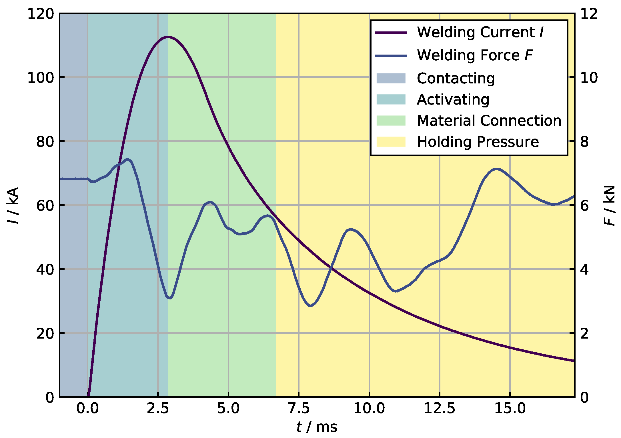
2. Capacitor Discharge Welding (CDW)

CDW belongs to the resistance welding processes and is mainly used for projection applications. Figure 1 shows, as an example, the welding current I and electrode force F as a function of time t for one of the conducted experiments. With the starting time t 0 ( t = 0   m s ) the current flow starts. At t p ( t = 3.6   m s ) the maximum current I of 113   k A is reached. At t h ( t = 7.1   m s ) the current decreased to 50% of its maximum, which is defined as the welding time [9].
Additionally Figure 1 shows four characteristic process phases, which are typical for steel alloys and were elaborated in [10,11]:
  • Contacting
    • Movement of electrodes onto the components
    • Increase of electrode force up to the predefined welding force
    • Plastic deformation in the contact area
  • Activating
    • Start of the current flow with high current density gradients
    • Very high power densities in contact area
    • Elimination of foreign and oxide layers
    • Activation of the contact surfaces
  • Material Connection
    • Follow-up of electrodes
    • Pressing together the activated surfaces
    • Development of material connection
    • Decreasing current and current density
    • Conductive heating of projection
    • Softening and plastic deformation of projection
  • Holding Pressure
    • Further follow-up of electrodes
    • Further decrease in current density
    • Further plastic deformation of projection
    • Enlargement of the connection area
    • Ending of follow-up of electrodes
    • Thermal conduction and cooling of joining zone
In comparison to spot welding with the medium-frequency inverter technique, projection welding with capacitor discharge has some complexities concerning the characteristic process phases:
  • Very high temperature gradients
  • High deformations of the projection
  • Activation of the contact surface by metal vapor

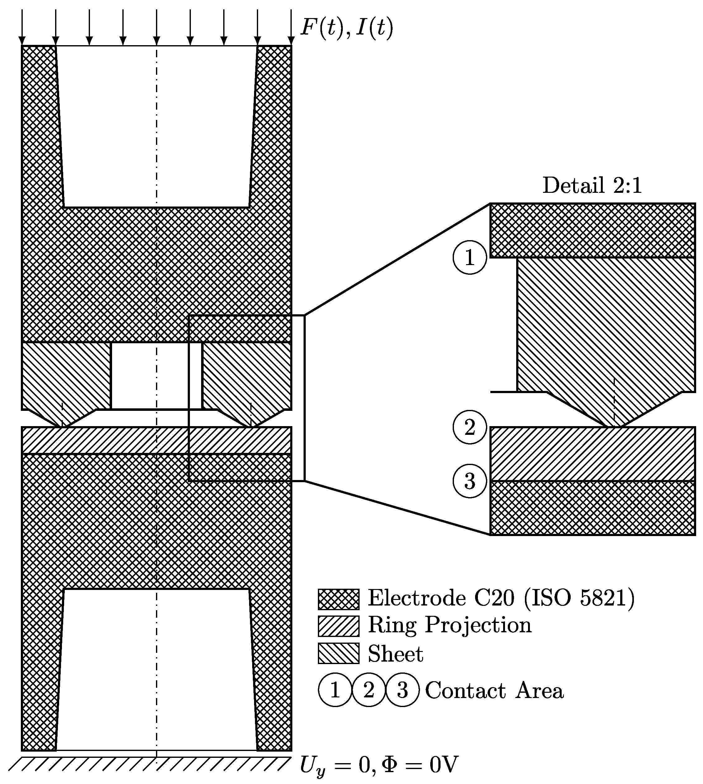
3. Finite Element Model

3.1. Geometry and Material Data

The technical drawing of the projection component is shown in Figure 2. The projection component is made of aluminium alloy EN-AW-6082. The thermophysical properties of the aluminium alloys were determined by a material simulation using the software JMatPro. The thermophysical properties of EN-AW-6082 are shown in Table A1 and the flow stress in Table A4. The geometric dimensions of the projection were optimized within a research project conducted also by the authors at Technische Universität Dresden [12]. The experimental data result in a recommendation of the width of the contact area of 0.5 m m and a projection angle of 120 . For the sheet component, the aluminium alloy EN-AW-5083 is used. The thermophysical properties of EN-AW-6082 are shown in Table A2 and the flow stress in Table A5. A common resistance welding electrode type C20 according to [13] is used. This electrode is made of CuCr1Zr. The thermophysical properties of CuCr1Zr are represented in Table A3 and the flow stress in [14].

3.2. Application Specific Modelling

The investigated 2D axisymmetric finite element model is shown in Figure 3. The quality of the mesh affects the solution of the simulation. Therefore, a geometry specific mesh is generated by analysing the convergence of the displacement. As a critical area, where the results have a big effect on the whole simulation, the penetration of the projection into the sheet is evaluated. The size of the elements was reduced until the penetration results did not change with further refinement of the mesh. This analysis was done at room temperature. The optimized element size in the contact area for this joining task is 0.0178 m m . With further distance from the contact area, the element size is growing.
From the numerical point of view, the edges of the projections contacting surface are singularities. The settings of the contact elements have to be chosen carefully to keep the difficulties under control coming with singularities. Therefore, the contact pressure of the joining zone was investigated at room temperature. The elaborated settings (key options) is shown in Table 1.
Adapting the model to the conditions at the beginning of the process enables a stable simulation until temperatures of about 600   K . However, with rising temperatures, and resulting from this the lowering of element stiffnesses as well as thermal expansion, the simulation terminates due to unconverged loadsteps of the structural physic. At the upper electrode the force F ( t ) and the current I ( t ) is applied as load from the measured data (Figure 1). As a boundary condition the displacement u y is blocked at the lower electrode and the electrical potential is 0 V . The uniform temperature T u n i is 298 K . There are three contact areas, which are made of contact and target elements:
  • Projection (Contact) - Electrode (Target)
  • Projection (Contact) - Sheet (Target)
  • Sheet (Contact) - Electrode (Target)
The behaviour of all contact surfaces is standard (not bonded, no roughness, no separation).

3.3. Implementation of Electrical Contact Resistance

There are many theories for calculating the ECR in resistance welding [15]. There is no validated theory for projection welding by capacitor discharge for aluminium components. The contact theory in [14,16] describes the ECR according to Equation (1). This theory has been validated for aluminium spot welding by the medium frequency inverter technique [17,18].
E C R ( T , σ c o n t ) = 3 d σ s ( T ) σ c o n t κ · ρ 1 ( T ) · ρ 2 ( T ) 2
The contact theory in [19] describes the ECR according to Equation (2). This theory has been validated for welding of steel and brass projections on steel sheets with a direct current.
E C R ( T , σ c o n t ) = 3 ξ σ s ( T ) σ c o n t κ · ρ 1 ( T ) · ρ 2 ( T ) 2 + ρ f i l m
The discussion of the contact theory in [19] is done by means of calculations with κ set to 0.5 . SONG inserts a parameter for the film resistance ρ f i l m . A good agreement with experiments is achieved. The pressure and temperature dependency of the ECR can also be described by the polynomial in Equation (3) with a varying exponent z. The author states the need of the variation in order to describe the temperature dependency of the pressure influence on the ECR. Transferring this insight to the application of Equation (2) in a coupled FE-model the variation of the exponent κ seems to be appropriate for modelling all phenomena taking place at the interfaces.
E C R = y σ c o n t z
Despite the different theoretical principles behind the theories, the effects of the exponent κ are similar. It balances the pressure against the temperature dependency of the ECR. It relates to the surface condition of the interfaces [14]. With progress in the simulation time, changes in the surfaces conditions are expectable from experimental investigations [10]. Therefore, a time-varying exponent corresponds to the phenomena in the real process. Namely, the disruption of surface film and flattening of asperities. For using the E C R as element parameter in the Ansys Mechanical simulation, the parameters E C C and T C C are necessary. E C C is calculated by Equation (4). T C C is calculated by Equation (5) with the Lorenz Number L of Equation (6) and the current temperature T of the element [14,16].
E C C = 1 E C R
T C C = L · T · E C C
L = 2.44 · 10 8 W Ω K 2

3.4. Indirect Coupling of a Numerical Simulation

There are two methods of coupling possible to model the interactions between structural, thermal and electrical phenomena. First, a direct coupling condenses the governing equations in one equation system. This is realized by the coupled field elements. By neglecting of the magnetic effects, the degrees of freedom are: the displacement u, the electric potential Φ and the temperature field T [20].
M ̲ ̲ 0 ̲ ̲ 0 ̲ ̲ 0 ̲ ̲ 0 ̲ ̲ 0 ̲ ̲ 0 ̲ ̲ 0 ̲ ̲ 0 ̲ ̲ u ¨ ̲ T ¨ ̲ Φ ¨ ̲ + C ̲ ̲ 0 ̲ ̲ 0 ̲ ̲ C t u ̲ ̲ C t ̲ ̲ 0 ̲ ̲ 0 ̲ ̲ 0 ̲ ̲ C v ̲ ̲ u ˙ ̲ T ˙ ̲ Φ ˙ ̲ + K ̲ ̲ K u t ̲ ̲ 0 ̲ ̲ 0 ̲ ̲ K t ̲ ̲ 0 ̲ ̲ 0 ̲ ̲ K v t ̲ ̲ K v ̲ ̲ u ̲ T ̲ Φ ̲ = F ̲ Q ̲ J ̲
Secondly, an indirect coupling uses more than one equation system while the coupling is executed by transferring results of one equation system to the other and vice versa. Two systems of equations are established with Equations (8) and (9) which will be solved individually. In this case, thermal–electrical effects are coupled direct while the coupling with structural phenomena is established indirect. This results in a separated modelling of the two different physics, thermal–electrical and structural. Investigations of welded joints show big deformations of the projection near the joining zone [20].
M ̲ ̲ u ¨ ̲ + C ̲ ̲ u ˙ ̲ + K ̲ ̲ u ̲ = F ̲
C t ̲ ̲ 0 ̲ ̲ 0 ̲ ̲ C v ̲ ̲ T ˙ ̲ V ˙ ̲ + K t ̲ ̲ 0 ̲ ̲ K v t ̲ ̲ K v ̲ ̲ T ̲ Φ ̲ = Q ̲ J ̲
Modelling big deformations with finite elements leads to disorted meshes, where bad qualities of the results or even unconverged loadsteps might result from [21]. Ansys Mechanical provides the methods of nonlinear adaptive meshing and rezoning to overcome those difficulties. For two-dimensional simulations, both methods are restricted to the solid structure elements PLANE182 and PLANE183 as well as the contact elements TARGE169, TARGE170, CONTA172 and CONTA174. However, to model thermal–electrical as well as structural effects other kinds of elements are needed (e.g., PLANE223). The separation of the physics provides the possibility to apply the rezoning method provided by the software at least for the structural physic. With the requirement of equally meshed physics used in an indirect coupled simulation, a way to transfer results of the thermal–electrical physic onto the new mesh still has to be found. The indirect coupling offers the following advantages:
  • Minimization of the computing effort
  • Adaptation of the solver to the requirements of each system of equations
  • Dynamic calculation of the contact resistance depending on the physic conditions without tabular precalculations (material data, temperature distribution and contact pressure)
  • Rezoning in structural physic (No rezoning for Coupled Field Elements)
Figure 4 shows the schematic process of the developed indirect simulation model. This is realized by a do loop. With the start of the simulation, the input data ( F ( t ) , I ( t ) ) were imported. The input data were provided by the measurements of the experiments as shown in Figure 1. After this, the two physical environments (structure and thermal–electric), short physics, were defined. At the beginning of the first iteration loop, the structure physic was read and solved. As a result, the contact pressure σ c o n t (normal stress in contact plane) of all contact zones was exported. This enables the first calculation of the electrical contact resistance (ECR) at room temperature (see Section 3.3). After calculating the ECR, the solution of the structure physic was saved and the thermal–electrical one was loaded. This was followed by an update of the geometry due to the temperature-dependent deformation and the solution. As a result, the temperatures of the nodes are exported and the solution of the thermal–electrical physic is saved. The next loop iteration follows by applying the temperature field from the thermal–electrical physic as a boundary condition to the structure physic. The rapid rise of the temperature leads to thermal expansion, softening of the elements and therefore to bigger deformations compared to room temperature. This results in a new contact situation, so that the ECR was updated with the new temperature field and the new contact pressures. These iteration steps Δ t were repeated until the current simulation time t n reached the end time t e n d of the simulation. Afterwards, the post-processing started. The physical environments were established by declaring the geometry of the model, meshing of this geometry, application of boundary conditions and solver settings. As mentioned above, the meshes of both physics have to be identical regarding the coordinates of the nodes and elements. Therefore, meshing has to be executed in the structural physic only. Afterwards, the established thermal–electrical physic built up onto the existing mesh by declaring different attributes to the elements. Both physics can be saved and loaded during the simulation as described in Figure 4. Within an indirect coupled simulation, special care has to be taken to the transfer of results between the physics:
  • To simulate the thermal–electrical phenomena with the current state of deformation, the calculated displacement in the structural physic is transferred by the UPGEOM command as a change of geometry.
  • Coupling in the contrary direction is implemented by applying the calculated temperatures as body loads by the LDREAD command. The temperatures are transferred to each node. Therefore the current state of thermal strain can be involved in the structural solution.
  • The coupling of effects within the contact zones was established by using the electrical contact conductivity E C C and the thermal contact conductivity T C C . Their values were calculated elementwise by Equations (4) or (5) and were therefore location-dependent. Before solving the thermal–electric physic starts, ECC and TCC were handed over to the contact elements by the RMODIF,,19 and RMODIF,,14 command respectively. Both parameters were declared as table arrays using the primary variable x-coordinate (2D) to guarantee every element gets their corresponding value.
The alternating calculation of the physics allows updating of the solver setting depending of the other physics than the one being solved. e.g., assuming large thermal strain with steeply rising temperatures the loadsteps and substeps of the structural solution might be chosen smaller when large changes of the temperature were detected in the thermal–electric solution.

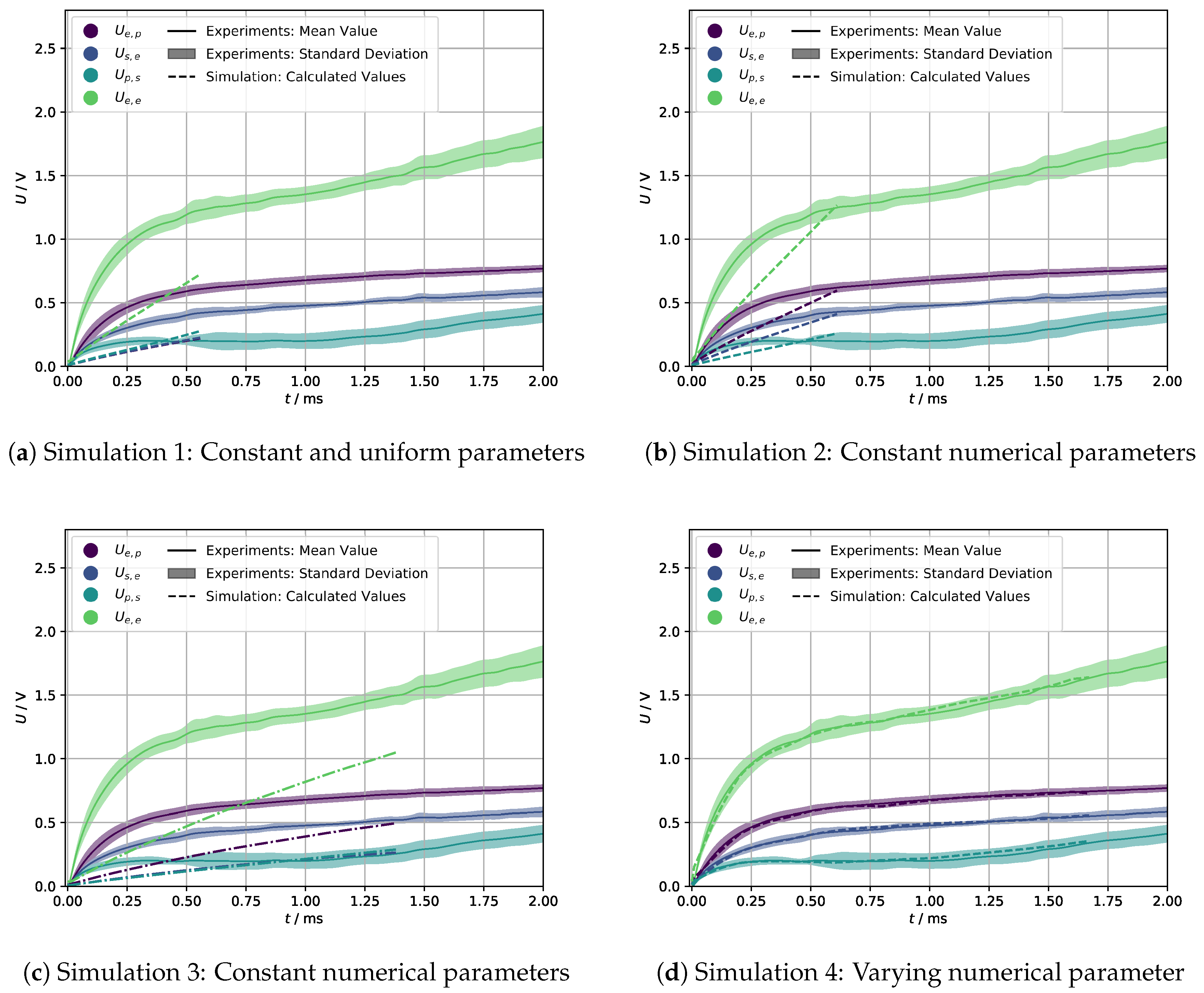
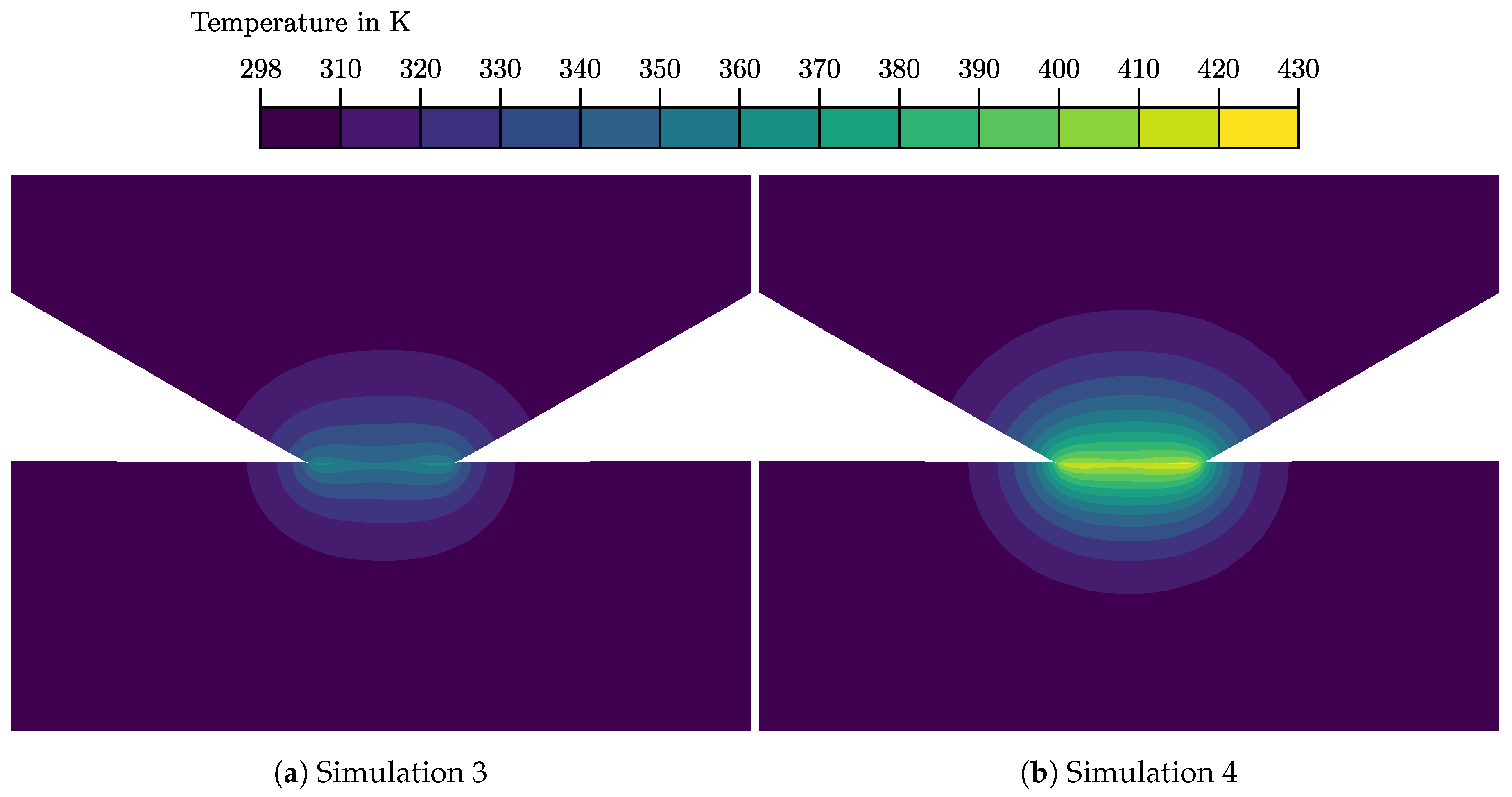
4. Results of the Indirect Process Simulation

4.1. Experimental Determination of the Electrical Voltage

In order to adapt the numerical factors of the contact theory, the electrical voltage drop was measured during the welding of the projection component (Figure 5a). Similar method for resistance spot welding of steel alloys was investigated by [22]. The voltage was measured at three positions (electrode-electrode U e , e ; projection-sheet U p , s ; sheet-electrode U s , e ). From these, the voltage drop at the electrode-projection U e , p interface was calculated.
The electrical voltage was measured with 1 M Hz and a resolution of 16 bit (measuring range from 0 V to 10 V ). Figure 5b shows the standard deviation of all (7) measured electrical voltages and the mean value. The sum of all individual voltages gives the total voltage between the electrodes U e , e . The measured voltage curves include inductivities. These were corrected according to [23]. The electrical voltage U p , s is lower than the others because the contact area is the smallest. Therefore, the contact pressure increases and the contact resistance decreases compared to the other contact zones (see Equation (2)). A strong increase of the individual voltage can be seen in the first 0.5 m s . Afterwards, the increase becomes flatter. The characteristic curve of U p , s is different to U e , p and U s , e .

4.2. Comparison of Experimental and Simulative Results

All simulations were executed until their termination due to convergence problems arising from large distortion of the mesh, low stiffnesses of elements with high temperatures and high contact pressure. The range of values for the numerical parameters d and κ used in the Equation (1) as well as ξ and κ in Equation (2) are declared by the authors SONG and WANG. It was not possible to calculate the measured voltages across the interfaces of the experiments within this range. The simulation results shown here were determined according to SONG (Equation (2) with ρ f i l m = 0 ). SONG recommends the numerical parameters ξ from 0.1 to 10 and κ from 0.5 to 1. In this range, the simulated electrical voltages were strongly outside the measurement. For this reason, the parameters were adapted to the measured voltages to reproduce the experiment. The new parameters are shown in Table A6 and Table A7. In simulation 1, 2 and 3 the value of κ was set to 1.
Uniformly defined values lead to a distribution of voltage drops, which is not consistent with the experiments. This is shown in Figure 6a. The three contact zones differ from each other regarding materials as well as the surface treatment and roughness. This implies that the numerical parameters should also be treated separately. This can be seen in Figure 6b–d. This results in a distribution of the simulated voltage drops at each contact as measured in the experiments. Figure 5b shows the characteristic voltage curves of the contacts U p , s , U e , p and U s , e are different from each other. The contacts are modelled with smooth surfaces. Therefore, it is not possible to include specific effects in the contact zone. One of these effects is the different behaviour of the asperities at the different contact surfaces, that is due to their different material characteristics. Furthermore, the behaviour of the surface films cannot be modelled, due to neglecting the specific film resistance ρ f i l m . To model the change of these effects, a time variable exponent κ is introduced. The simulation results in Figure 6b,c show that a constant set of numerical parameters does not lead to the measured voltages over process time. Either the simulated voltage, or their gradient does not match the experimental results. For bigger values of the factor ξ in Equation (2), the strong increase of voltage drops at the beginning of the process can be modelled. It results in a moment of time where the calculated voltages exceed the measured values while maintaining their high gradient. After this point of time, the values of the simulation were constantly to big. Choosing low values results in not reaching the measured voltages at all. With κ = 1 , the voltages are smaller then the experimental values. If κ < 1 , the voltages become bigger. Therefore, the values of the exponent are changed as shown in the Table A6. Figure 6d shows the effect of the final configuration of κ . With the simulation, four values were found which can model the experimental measured voltages in a satisfying manner. The simulation terminated at a time of 1.67   m s and a maximum temperature of 671   K located in the joining zone. The convergence problems were due to thermal expansion and low element stiffnesses resulting from high temperature. This is accompanied by large deformations.

5. Discussion

With the elaboration of the FEM model in this work the most suitable settings where found regarding the mesh quality, calculation methods, boundary conditions and contact settings. Additionally assuming correct material data one can make the assumption that the numerical errors in the results are neglectable for this type of investigation. Because of this, the only way to reproduce the measured voltages is to adapt the contact resistance. For the reason of adaption the authors of contact the resistance models discussed in this work already included parameters to be changed in their equations. Taking advantage of this, it is possible to reach very good agreement of the FEM simulation with the real process regarding the electrical phenomena. By calculating the thermal conductance from the electrical conductance by the commonly used Wiedemann-Franz-Law the quality of the electrical results applies for the thermal phenomena too.
The results show big influence of the numerical parameters on the whole simulation. Thus they are critical for the quality of the simulation results and further investigations. Figure 7a,b show the temperature distribution within the joining zone at a process time of 0.75   m s . From Figure 6c,d it can be seen, that the current values of the voltage are nearly the same (Simulation 3: U = 0.17   V ; Simulation 4: U = 0.20   V ). Contrarily their time history is very different. This results in a huge change of the temperature distribution. This shows the relevance of adapting the contact resistance over the whole process time.
It was already stated that the adaption of the numerical parameters has to be done according to the characteristics of the contacting surfaces. With change of this characteristics e.g. by using different materials, surface roughness or different surface treatments it is necessary to adapt the numerical parameters recursively. Thus the quality of the simulation results is not only dependent from the numerical modelling methods but also highly influenced by the calibration of the contact resistance parameters.
All in all, a separated treatment of the contact resistance calculation at each contact, as well as the implementation of time dependent, numerical parameters allows the reproduction of the experiments concerning the thermal-electric and structural aspects. By interpreting the adaption of the numerical parameters, future investigations might show further insights into contact resistance effects not implemented by physical parameters in Equation (2).

6. Conclusions

Despite the discontinuous geometry of the projection an indirect coupled model, allowing stable and efficient simulation of the CDW-process up to 671   K was built. With a reasonable adaption of the numerical parameters to the experimental measured voltages the simulation time was extended from 0.57 m s to 1.67 m s . Furthermore, the indirect coupling allows the dynamic calculation of the contact resistance and therefore a suitable way of determining the numerical parameters. A set of parameters was found, which yields to voltage drops at the contacts as measured in experiments. Therefore, it is possible to consider effects which can’t be seen using constant factors, such as the evolution of surface conditions during the process. For the first time, this provides the possibility to adapt the simulation model to the complexity (large deformations, short current rise times and high temperature gradients) of the CDW. The presented model cannot describe the CDW process completely due to convergence problems. The convergence problems appear because of the high deformation at high temperatures. The finite elements deform heavily on the edge of the projection area. Additionally, the contact settings have been determined at room temperature, and therefore might be inadequate for high temperatures. Furthermore, rezoning was evaluated as a method to possibly overcome convergence issues within the structural physic [24].

Author Contributions

Conceptualization, J.K., M.B. and S.H.; methodology, J.K. and M.B.; software, J.K. and M.B.; validation, J.K. and M.B.; formal analysis, M.B.; investigation, J.K. and M.B.; resources, J.K.; data curation, M.B.; writing—original draft preparation, J.K.; writing—review and editing, J.K., S.H., M.B. and J.Z.; visualization, J.K. and M.B.; supervision, U.F.; project administration, J.Z.; funding acquisition, J.Z. All authors have read and agreed to the published version of the manuscript.

Funding

This research was funded by the Deutsche Forschungsgemeinschaft (DFG, German Research Foundation) within the project “Basic investigations for the in-situ simulation of resistance spot welding processes” under the grant numbers FU 307/15-1 resp. IH 124/17-1, Project-no.: 389519796.

Conflicts of Interest

The authors declare no conflict of interest.

Abbreviations

The following abbreviations are used in this manuscript:
CDWCapacitor Discharge Welding
ECCElectrical Contact conductivity
ECRElectrical Contact Resistance
TCCThermal Contact Conductivity

Appendix A. Thermophysical Properties for Numerical Simulation

Table A1. Thermophysical properties of EN-AW-6082.
T/K ρ /kg m 3 E/GPa ν /1 α /K 1 10 5 λ /W m 1 K 1 c p /J kg 1 K 1 h/MJ m 3 ρ el / μ Ω m
2982697.7068.2720.338Reference192.626-260.036
3032696.8268.1150.3382.240193.097901300.037
3232693.1667.4590.3392.261194.812913380.039
3432689.4566.7860.3392.282196.209924880.041
3732683.7765.7420.3412.313197.8139401620.044
4032677.9664.6580.3422.344198.9389542380.047
4332672.0363.5350.3432.375199.6779673140.050
4732663.9361.9750.3452.417200.1779854170.055
5032657.7160.7590.3472.449200.2529974950.058
5332651.3759.5030.3492.480200.11410105740.062
5732642.7357.7660.3512.523199.64410276800.067
6032636.1156.4170.3532.555199.10710397590.070
6332629.3755.0280.3552.587198.43310528400.074
6732620.2153.1130.3572.630197.34410699480.079
7032613.2151.6300.3592.662196.401108210300.083
7332603.6949.5910.3622.706194.991110311400.089
7732596.4248.0140.3642.738193.832112112230.093
8032589.0546.3980.3672.771192.592114013070.097
8332577.9637.1020.3752.895184.616159814470.107
8732556.8625.7370.3883.194171.884218516290.122
9032520.7410.5270.4123.869146.974726618610.144
9332393.110.0000.5006.68388.391117325340.232
9732380.010.0000.5006.59389.735117326320.239
11732311.830.0000.5006.36096.456117330990.268
13732239.980.0000.5006.337103.177117335280.293
15732165.500.0000.5006.426109.897117339190.315
17732089.330.0000.5006.581116.618117342720.334
20731973.730.0000.5006.889126.699117347310.360
22731896.830.0000.5007.127133.420117349930.375
27731709.330.0000.5007.788150.222117355030.406
32731533.480.0000.5008.507167.023117358370.431
Table A2. Thermophysical properties of EN-AW-5083.
T/K ρ /kg m 3 E/GPa ν /1 α /K 1 10 5 λ /W m 1 K 1 c p /J kg 1 K 1 h/MJ m 3 ρ el / μ Ω m
2982632.5769.2180.332Reference140.998-310.048
3032631.7069.0580.3322.258141.745911430.049
3232628.1068.3870.3322.279144.618923910.051
3432624.4567.6980.3332.300147.2019341390.053
3732618.8666.6310.3352.331150.6239502130.057
4032613.1665.5220.3362.362153.5949642870.060
4332607.3364.3730.3372.393156.1939773620.063
4732599.3762.7770.3392.435159.1769954640.068
5032593.2661.5310.3412.467161.10510075400.071
5332587.0360.2450.3422.498162.80310206180.075
5732578.5558.4660.3452.541164.74810377220.080
6032572.0657.0840.3462.573165.99210508000.083
6332565.4555.6610.3482.605167.06610628790.087
6732556.4653.6990.3512.647168.25310809860.092
7032549.5952.1800.3532.680168.973109310660.096
7332537.2939.3710.3702.878167.104119211760.105
7732525.2635.0410.3752.983166.138128312940.112
8032514.9531.0110.3803.088164.219141613890.117
8332502.3125.6320.3863.244160.279170714960.124
8732474.0913.7550.4043.714146.047333516950.141
9032404.570.7500.4545.225108.6601619420860.187
9332335.980.0000.5006.66687.261118724630.235
9732323.110.0000.5006.58088.670118725590.241
11732256.010.0000.5006.36095.713118730210.270
13732185.180.0000.5006.349102.757118734450.294
15732111.680.0000.5006.450109.801118738310.315
17732036.440.0000.5006.616116.845118741780.334
20731922.240.0000.5006.940127.411118746280.358
22731846.280.0000.5007.188134.455118748840.372
27731661.180.0000.5007.876152.064118753800.401
32731487.850.0000.5008.621169.674118757020.424
Table A3. Thermophysical properties of CuCr1Zr.
T/K ρ /kg m 3 E/GPa ν /1 α /K 1 10 5 λ /W m 1 K 1 c p /J kg 1 K 1 h/MJ m 3 ρ el / μ Ω m
298888287.80.326Reference32639000.021
473880381.00.2981.6503053936230.033
5738755--1.7202913959680.039
673-77.00.279-----
7738656--1.80028140016600.054
87369.60.230-----
9738549--1.89027548228200.070
107365.10.238-----
1173842560.60.2122.02026849436800.098

Appendix B. Flow Stress Data for Numerical Simulation

Table A4. Flow Stress of EN-AW-6082.
ϵ /1 σ T /MPa
σ 298 K σ 333 K σ 373 K σ 433 K σ 473 K σ 533 K σ 573 K σ 673 K σ 773 K σ 873 K
0165.6162.4159.0152.9148.2140.3134.687.4106.663.6
0.02215.0214.0217.6232.0227.5194.2175.1136.0106.672.7
0.04232.3232.2239.0255.7227.4194.2175.1136.0106.672.7
0.06243.5244.0252.9254.8227.2194.2175.1136.0106.672.7
0.08251.9252.9263.5253.5226.7194.2175.0136.0106.672.7
0.1258.6260.0272.0252.1226.0194.1175.0136.0106.672.7
0.15271.4273.6288.4248.9224.0193.8174.9136.0106.672.7
0.2280.9283.8300.7246.4222.1193.3174.7136.0106.672.7
0.25288.5291.9303.5244.3220.5192.6174.4136.0106.572.7
0.3294.9298.8301.2242.6219.2191.8174.0135.9106.572.6
0.35300.5304.7299.2241.2218.0191.1173.6135.8106.472.6
0.4305.4310.0297.4239.9216.9190.4173.1135.7106.372.5
0.45309.7314.7295.9238.8216.0189.8172.6135.5106.172.5
0.5313.7318.9294.5237.8215.2189.2172.2135.3106.072.4
0.6320.7326.4292.1236.0213.7188.2171.4135.0105.672.2
0.7326.8332.9290.1234.5212.5187.2170.7134.6105.371.6
0.8332.1338.7288.3233.3211.4186.4170.0134.3105.070.9
0.9336.9343.8286.8232.1210.5185.7169.4134.0104.670.3
1341.2344.5285.4231.1209.6185.1168.9133.6104.469.7
2371.1333.0276.6224.7204.1180.7165.3131.4102.365.4
Table A5. Flow Stress of EN-AW-5083.
ϵ /1 σ T  /  M Pa
σ 298 K σ 333 K σ 373 K σ 433 K σ 473 K σ 533 K σ 573 K σ 673 K σ 773 K σ 873 K
0.00179.1176.0172.6166.7162.1154.4148.893.7103.112.6
0.02227.4226.3229.9243.8259.3217.3192.0142.0103.129.5
0.04244.5244.3250.9274.2261.8217.3192.0142.0103.129.5
0.06255.5256.0264.6294.5261.5217.3192.0142.0103.129.5
0.08263.8264.7275.0297.1260.8217.3192.0142.0103.129.5
0.10270.4271.7283.4295.1259.8217.2192.0142.0103.129.5
0.15283.0285.1299.4290.6256.9216.8191.8142.0103.129.5
0.20292.3295.1311.4287.0254.3216.0191.6142.0103.129.5
0.25299.8303.1321.0284.1252.0215.0191.1141.9103.129.5
0.30306.0309.8329.2281.7250.1213.9190.5141.8103.029.5
0.35311.5315.5336.2279.6248.4212.9189.9141.6102.829.4
0.40316.2320.6342.4277.8246.9212.0189.2141.5102.729.4
0.45320.5325.2348.0276.2245.6211.1188.6141.2102.529.4
0.50324.4329.4353.0274.8244.4210.2188.0141.0102.229.3
0.60331.2336.7349.5272.3242.3208.7186.8140.5101.829.2
0.70337.1343.0346.7270.2240.6207.4185.8140.0101.329.1
0.80342.2348.6344.2268.4239.1206.3184.9139.5100.929.1
0.90346.9353.6342.0266.8237.7205.2184.0139.0100.529.0
1.00351.1358.1340.1265.4236.5204.3183.3138.6100.128.9
2.00380.0389.4327.5256.3228.7198.2178.1134.397.328.4

Appendix C. Simulation Values for Numerical Parameters

Table A6. Values of numerical parameter ξ in Simulation 1 to 4.
# Simulation ξ e , p ξ s , e ξ p , s
10.00250.00250.0025
20.00800.00500.0020
30.00300.00100.0005
40.00300.00200.0005
Table A7. Values of numerical parameter κ in Simulation 4.
t/ms κ e , p κ p , s κ s , e
0.00.9000.850.900
0.20.9050.880.910
0.40.9250.920.930
0.60.9400.960.942
0.80.9550.980.955
1.00.9621.000.965
1.20.9701.000.975
1.40.9771.000.982
1.60.9851.000.990
1.81.0001.001.000
>1.81.0001.001.000

References

  1. Florea, R.; Bammann, D.; Yeldell, A.; Solanki, K.; Hammi, Y. Welding parameters influence on fatigue life and microstructure in resistance spot welding of 6061-T6 aluminum alloy. Mater. Des. 2013. [Google Scholar] [CrossRef]
  2. Qiu, R.; Iwamoto, C.; Satonaka, S. Interfacial microstructure and strength of steel/aluminum alloy joints welded by resistance spot welding with cover plate. J. Mater. Process. Technol. 2009. [Google Scholar] [CrossRef]
  3. Zhang, W.; Qiu, X.; Sun, D.; Han, L. Effects of resistance spot welding parameters on microstructures and mechanical properties of dissimilar material joints of galvanised high strength steel and aluminium alloy. Sci. Technol. Weld. Join. 2011. [Google Scholar] [CrossRef]
  4. Duderstadt, F.; Hömberg, D.; Khludnev, A.M. A mathematical model for impulse resistance welding. Math. Methods Appl. Sci. 2003, 26, 717–737. [Google Scholar] [CrossRef]
  5. Hömberg, D.; Duderstadt, F.; Dreyer, W. Modelling and Simulation of Capacitor Impulse Welding. Math. Key Technol. Future 2003. [Google Scholar] [CrossRef]
  6. Casalino, G.; Panella, F. Numerical Simulation of Multi-Point Capacitor Discharge Welding of AISI 304 Bars. Proc. Inst. Mech. Eng. Part B J. Eng. Manuf. 2006, 220, 647–655. [Google Scholar] [CrossRef]
  7. Casalino, G.; Ludovico, A. Finite element simulation of high speed pulse welding of high specific strength metal alloys. J. Mater. Process. Technol. 2008, 197, 301–305. [Google Scholar] [CrossRef]
  8. Cavaliere, P.; Dattoma, V.; Panella, F. Numerical analysis of multipoint CDW Welding Process on stainless AISI304 steel bars. Comput. Mater. Sci. 2009, 46, 1109–1118. [Google Scholar] [CrossRef]
  9. Deutscher Verband für Schweißen und Verwandte Verfahren e.V.: Kondensatorentladungsschweißen—Grundlagen, Verfahren und Technik (DVS 2911); Deutscher Verband für Schweißen und Verwandte Verfahren e.V.: Düsseldorf, Germany, 2016.
  10. Ketzel, M.M.; Hertel, M.; Zschetzsche, J.; Füssel, U. Heat development of the contact area during capacitor discharge welding. Weld. World 2019, 63, 1195–1203. [Google Scholar] [CrossRef]
  11. Zschetzsche, J.; Ketzel, M.M.; Füssel, U.; Rusch, H.J.; Stocks, N. Process Monitoring at Capacitor Discharge Welding. ASNT Res. Symp. 2019. [Google Scholar] [CrossRef]
  12. Ketzel, M.M.; Koal, J.; Zschetzsche, J.; Füssel, U. Buckelschweißen von Aluminiumlegierungen Mittels Kondensatorentladungsschweißen mit Veränderlicher Kraft und Kraftgesteuertem Auslösen der Entladung (IGF-Nr.: 19.889 B); Schlussbericht; Forschungsvereinigung Schweißen und verwandte Verfahren e.V. des DVS: Düsseldorf, Germany, 2020. [Google Scholar]
  13. DIN EN ISO 5821:2009-04. Resistance Welding—Spot Welding Electrode Caps (ISO 5821:2009). 2009. Available online: https://www.beuth.de/en/help/citing-din-standards (accessed on 23 September 2020).
  14. Wang, J.; Wang, H.P.; Lu, F.; Carlson, B.E.; Sigler, D.R. Analysis of Al-steel resistance spot welding process by developing a fully coupled multi-physics simulation model. Int. J. Heat Mass Transf. 2015, 89, 1061–1072. [Google Scholar] [CrossRef]
  15. Hamedi, M.; Atashparva, M. A review of electrical contact resistance modeling in resistance spot welding. Weld. World 2017, 61, 269–290. [Google Scholar] [CrossRef]
  16. Wan, Z.; Wang, H.P.; Wang, M.; Carlson, B.E.; Sigler, D.R. Numerical simulation of resistance spot welding of Al to zinc-coated steel with improved representation of contact interactions. Int. J. Heat Mass Transf. 2016, 101, 749–763. [Google Scholar] [CrossRef]
  17. Tuchtfeld, M.; Heilmann, S.; Füssel, U.; Jüttner, S. Comparing the effect of electrode geometry on resistance spot welding of aluminum alloys between experimental results and numerical simulation. Weld. World 2019, 63, 527–540. [Google Scholar] [CrossRef]
  18. Deng, L.; Li, Y.; Cai, W.; Haselhuhn, A.S.; Carlson, B.E. Simulating thermoelectric effect and its impact on weld nugget asymmetric growth in aluminum resistance spot welding. J. Manuf. Sci. Eng. 2020, 142, 091001. [Google Scholar] [CrossRef]
  19. Song, Q. Testing and Modeling of Contact Problems in Resistance Welding. Ph.D Thesis, Technical University of Denmark, Kongens Lyngby, Denmark, 2003. [Google Scholar]
  20. ANSYS Inc. Electro-Thermo-Structural Analysis; MAPDL 2020 R1 Theory References, 10.1.2.7.; Ansys Inc.: Canonsburg, PA, USA, 2020. [Google Scholar]
  21. Wehle, M. Basics of Process Physics and Joint Formation in Resistance Projection Welding Processes Welding. Ph.D Thesis, Institute for Materials Science, Universität Stuttgart, Stuttgart, Germany, 2020. [Google Scholar]
  22. Kaars, J.; Mayr, P.; Koppe, K. Generalized dynamic transition resistance in spot welding of aluminized 22MnB5. Mater. Des. 2016, 106, 139–145. [Google Scholar] [CrossRef]
  23. Ketzel, M.M.; Zschetzsche, J.; Füssel, U. Elimination of voltage measuring errors as a consequence of high variable currents in resistance welding. Weld. Cut. 2017, 16, 164–168. [Google Scholar]
  24. Long, F.X. Development of a Remeshing Method for the Finite-Element Simulation of a Capacitor Discharge Press Fit Welding Process. Master’s Thesis, Karlsruher Institut für Technologie, Karlsruhe, Germany, 2018. [Google Scholar]
Figure 1. Characterization of a capacitor discharge welding process and input data for simulation.
Processes 08 01330 g001
Figure 2. Technical drawing of the investigated ring projection.
Processes 08 01330 g002
Figure 3. The investigated 2D axisymmetric finite element (FE) model with the applied loads and boundary conditions. Detailed view of the contact areas and the investigated ring projection.
Processes 08 01330 g003
Figure 4. Schematic sequence of an indirect coupled numerical simulation in Ansys Mechanical APDL.
Processes 08 01330 g004
Figure 5. Schematic representation of the experimental setup (a) and the mean value with standard deviation of the measured voltage of all contact areas (b).
Processes 08 01330 g005
Figure 6. Effect of the numerical parameters ξ and κ (Table A6 and Table A7) on the simulated electric voltage curve and comparison with the experimental data.
Processes 08 01330 g006
Figure 7. Temperature T distribution at t = 0.75 ms.
Processes 08 01330 g007
Table 1. Settings of the contact elements TARGE169 and CONTA172.
#DescriptionChosen Setting (Related Value)
1Degree of freedomDisplacement in x- and y-direction (0)
2Contact algorithmAugmented Lagrange (0)
4Location of contact detectionProjection method (3)
5Automated adjustmentNo adjustment (0)
6Contact stiffness variationNominal refinement (1)
7Time incrementation controlReasonable time increments (2)
10Contact stiffness updateEach iteration (0)
12Behaviour of contact surfaceStandard (0)
18Sliding behaviourFinite sliding (0)
Publisher’s Note: MDPI stays neutral with regard to jurisdictional claims in published maps and institutional affiliations.

