Abstract
A novel bridgeless isolated AC LED driver is developed, which improves LED utilization and application flexibility due to a coupled inductor inserted between the bidirectional switch and the LED module without any output electrolytic capacitor. By reducing the turns ratio of the coupled inductor, the voltage across the secondary side will be decreased so as to lessen the voltage across the LED strings and hence reduce the number of LEDs, thereby making the load design of the AC LED driver more flexible. It is noted that the coupled inductor plays a role of not only galvanic isolation but also inductor behavior as well as transformer behavior. Therefore, during the turn-on period of the bidirectional switch, the coupled inductor can transfer the energy to one LED string and store the energy simultaneously, whereas during the turn-off period of the bidirectional switch, the coupled inductor can release the stored energy to the other LED string. That is, two LED strings are conducted over a pulse-width-modulated (PWM) period for any half-cycle, implying that LED utilization is upgraded. As for LED dimming, it is realized by directly tuning the control signal for the bidirectional switch without any dimming circuit. Eventually, the basic operating principles and theoretical deductions are given along with some experimental results provided to verify the effectiveness of the proposed AC LED driver topology.
1. Introduction
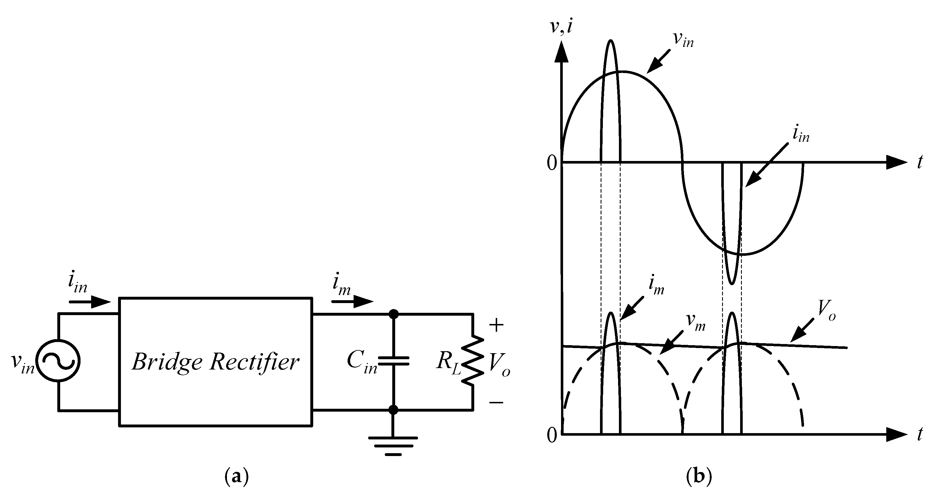
Conventionally, the basic characteristic of LEDs is a unidirectional direct current (DC) operation. In order for the LED to operate normally under alternating current (AC), it must be driven by converting the AC input voltage into the DC output voltage through conversion devices such as transformers, rectifiers, etc. [1]. The conventional method is to connect the AC input source to a bridge rectifier. As shown in Figure 1a, without a stabilized filter capacitor Cin, the AC voltage with a sine wave will get a waveform of vm after bridge rectification, as shown in Figure 1b. Therefore, a large capacitor is connected in parallel to obtain a DC voltage Vo with relatively small ripple. However, this approach can only briefly turn on the diodes of the bridge rectifier when the input AC voltage is higher than the voltage across this large capacitor. At this time, the input current becomes a pulse-shaped non-ideal sine wave, causing harmonic distortion, and there is a phase difference between the voltage and current, resulting in a low power factor (PF). Therefore, the harmonic interference of the mains bus and the unnecessary power loss are increased, thereby reducing the utilization rate of the power supply and increasing the operating cost of the mains.
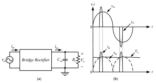
Figure 1.
Conventional bridge rectifier: (a) structure; (b) waveforms.
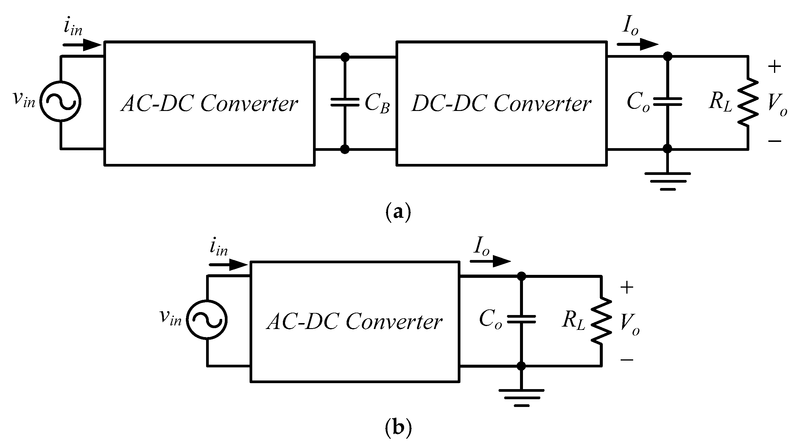
Although the conventional AC LED driving circuit has low cost and simple structure, the problem of harmonic distortion of its input current still exists. Therefore, many power-factor-corrected (PFC) circuits have been developed to reduce the current harmonic and to improve the power factor. The PFC circuit can be mainly classified into two types: passive and active. The latter can be divided into two-stage [1,2,3,4,5,6] and single-stage [1], as shown in Figure 2. Although the two-stage PFC circuit has advantages of high PF and stable output voltage, it has one more energy conversion and one more control circuit than the single-stage PFC one. This will increase the loss of energy conversion, more components, and more circuits. Accordingly, the single-stage PFC circuits are generally used in low-to-medium power products.

Figure 2.
Conventional AC-DC converter: (a) two-stage; (b) single-stage.
However, all the above-mentioned AC-DC converters drive LEDs in the DC form. In addition, if the LEDs are properly arranged, combined and controlled, the AC power supply can directly drive LEDs [1]. There are two types of AC LED drivers. One is that the AC voltage is bridge-rectified and then feeds the series LEDs that are connected in series with a resistor to limit the current, as shown in Figure 3. The other is that two LED strings with the same number of LEDs are connected in parallel with opposite polarities, arranged in a structure similar to bridge rectification, and then connected in series with a current-limiting resistor, as shown in Figure 4.
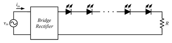
Figure 3.
AC LED with bridge rectifier.
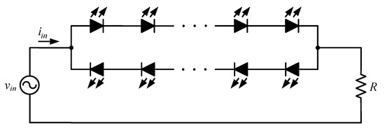
Figure 4.
AC LED without bridge rectifier.
The advantage of the methods shown in Figure 3 and Figure 4 is that the LED can be directly driven by an AC power source, so there is no need to use a converter for energy conversion, reducing the size and cost of the LED driver. However, due to the influence of the characteristics of the LED itself, the more the LEDs on the string, the greater is the forward conduction voltage and the more serious is the input current distortion. Consequently, the segmental AC LED drivers [7,8,9,10,11,12] are presented to improve PF and THD. As shown in Figure 5, this segmental AC LED driver [9] performs a good result in THD and PF. As far as the LED driver is concerned, in addition to providing a stable power supply to make the LED light up steadily, it also needs to have a dimming function that can adjust the brightness.
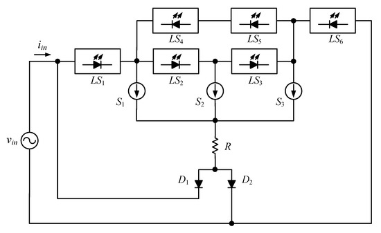
Figure 5.
Segmental AC LED driver.
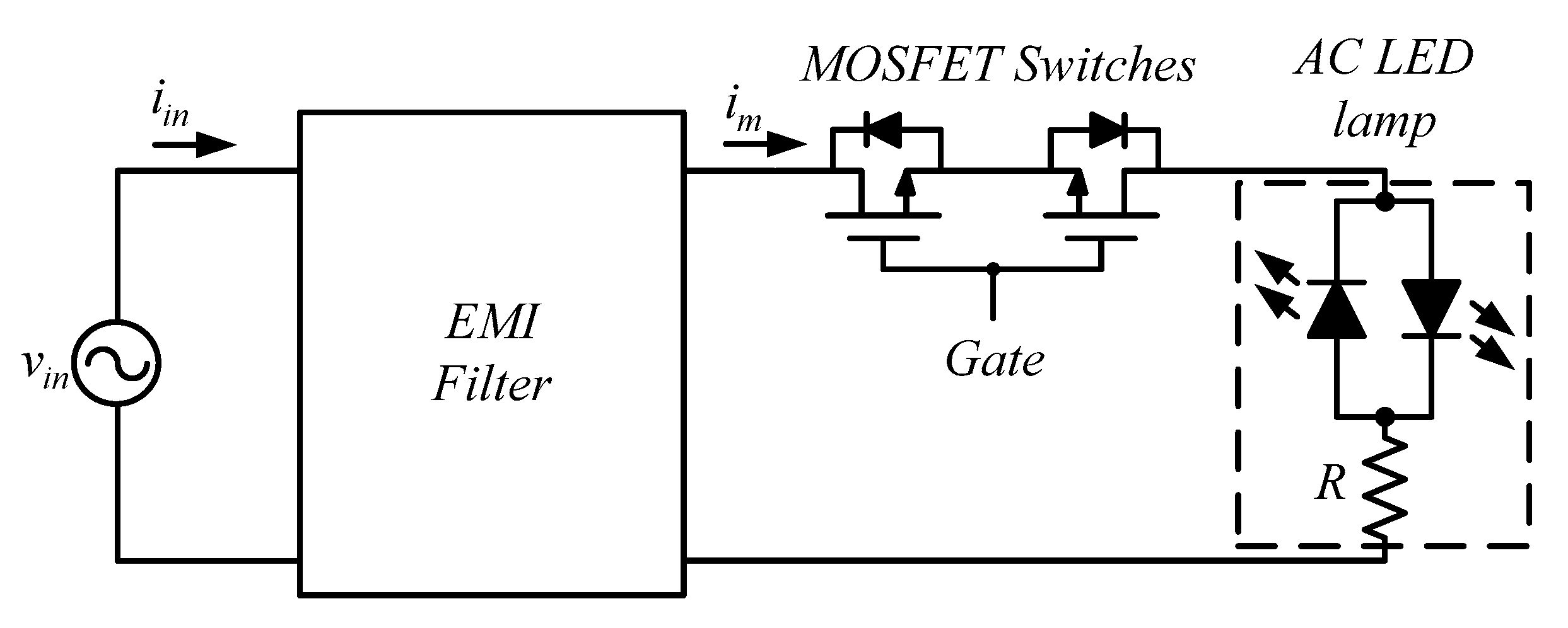
The literature [13] presents an AC LED driving circuit that uses two active switches for LED dimming, as shown in Figure 6. This structure consists of two active switches, called a bidirectional switch, and an electromagnetic interference (EMI) filter used to eliminate high-frequency noise. Since the gates and sources of the two switches are respectively connected to each other, it is possible to simply use one gate driving signal to drive the two switches at the same time. As shown in Figure 7, by adjusting the on-time of the switches, the average value of the output voltage is changed, and therefore the LED dimming can be achieved. However, when the switches are turned on, because the input voltage is directly connected to the LED string, the LED string must increase the number of LEDs to increase LED string withstand voltage so as to avoid being burned out in the vicinity of the input voltage peak. Consequently, the number of LEDs is limited by the withstand voltage, causing difficulties in the design of a small number of LEDs. In addition, this driving method of the LED string is that one string is driven when the input voltage is positive and the other string is driven when the input voltage is negative, that is, only a single string is driven in one half-cycle. This will reduce the utilization rate of LEDs.
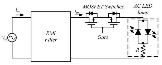
Figure 6.
PWM dimming circuit for AC LED lamp.
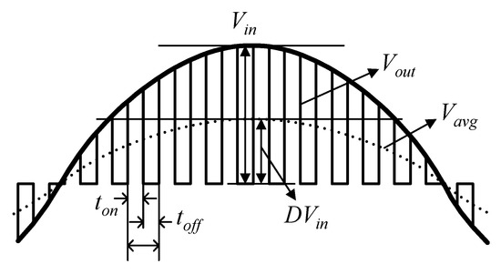
Figure 7.
Input voltage, output voltage and average output voltage.
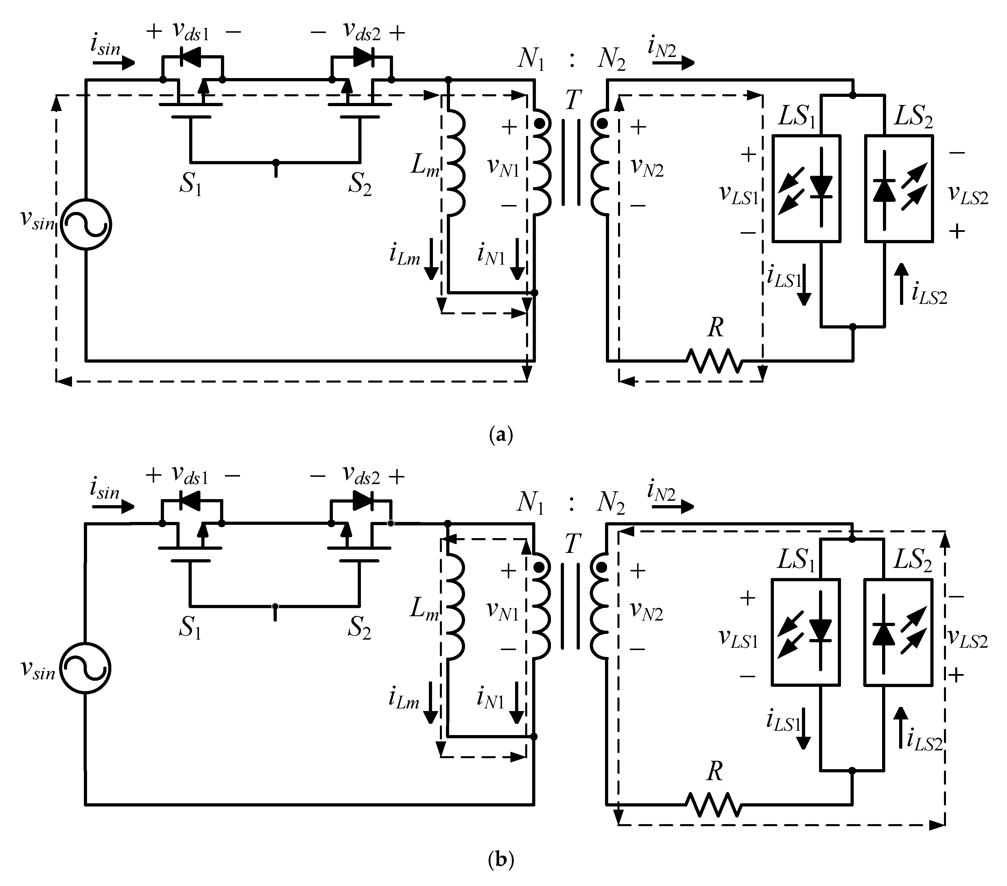
In view of the abovementioned, the proposed AC LED driver is based on the literature [13] to improve the flexibility and utilization of the number of LED strings, so a coupled inductor is added between the bidirectional switch and the AC LED module as shown in Figure 8. By changing the turns ratio of the coupled inductor, the voltage on the secondary side of the coupled inductor is reduced so that the voltage across the AC LED module can be reduced, and hence the number of LEDs on the string can also be reduced. This also increases the design flexibility. Unlike the flyback coupled inductor, the coupled inductor has transformer behavior and transfers energy to make one LED string turn on when the switch is turned on. Moreover, since the coupled inductor also has inductor behavior, the coupled inductor demagnetizes and turns on the other LED string when the switch is turned off. Therefore, both the forward and reverse LED strings will be turned on once over one PWM period for any half-cycle, so as to improve the utilization rate of LEDs.
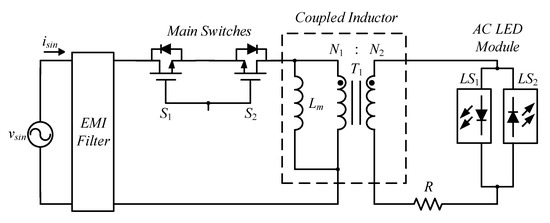
Figure 8.
Proposed AC LED driver.
2. System Configuration of the Proposed AC LED Driver
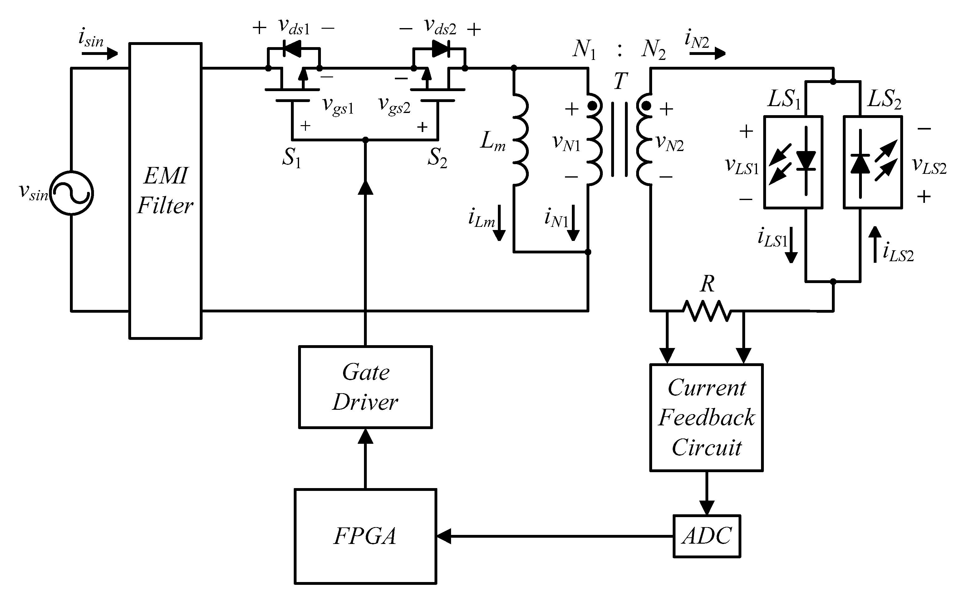
Figure 9 shows the proposed AC LED driver, which is constructed by a bidirectional switch built up by two main switches S1 and S2, one coupled inductor T, which is established by one magnetizing inductance Lm and one ideal transformer, two LED strings LS1 and LS2, and one current-limiting feedback resistor, R. Furthermore, the bidirectional switch is directly controlled to achieve LED dimming; hence, this can remove the unnecessary dimming circuit. As for the feedback control loop, it contains the current feedback circuit, the analog-to-digital converter (ADC), and the field programmable gate arrays (FPGA). As for the EMI filter, it is used to eliminate high-frequency noise.
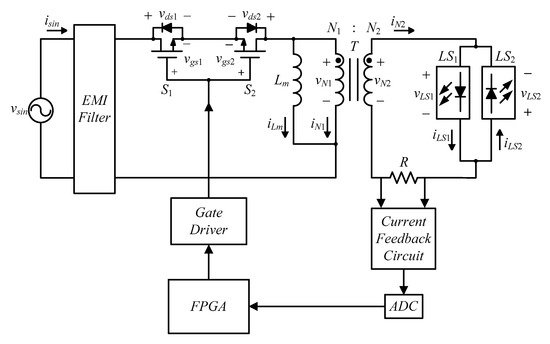
Figure 9.
System configuration of the proposed AC LED driver.
3. Operating Principles
In order to facilitate analysis, some assumptions and symbols are first given:
- (1)
- The bidirectional switch is regarded as an ideal component;
- (2)
- Each LED is an ideal component, and its forward conduction voltage is a constant value. Hence, under the same number of LEDs, the voltages across the LED strings LS1 and LS2 are the same;
- (3)
- The leakage inductance effect of the coupled inductor T is ignored;
- (4)
- If the input voltage is at the peak of the input voltage, then this driver operates in the boundary conduction mode (BCM); otherwise, in the discontinuous mode (DCM);
- (5)
- The turns ratio n between the primary winding N1 and the secondary winding N2 is n = N1/N2;
- (6)
- vsin, vgs1, vgs2, vds1, vds2, vLS1, and vLS2 are used to represent the AC input voltage, the gate driving signal for S1, the gate driving signal for S2, the voltage on S1, the voltage on S2, the voltage across LS1, and the voltage across LS2, respectively;
- (7)
- isin, iLm, iN1, iN2, iLS1, and iLS2 are used to denote the AC input current, the magnetizing current, the primary transferring current, the secondary transferring current, the current in LS1, and the current in LS2, respectively; and
- (8)
- D is the duty cycle, DTs is the turn-on time, (1−D)Ts is the magnetization turn-off time for BCM, and Δ1Ts is the magnetization turn-off time for DCM.
Figure 10 shows the relationship between the magnetizing inductor current iLm and the LED string currents iLS1 and iLS2. Due to the different conduction times of the LED strings and the operating mode (BCM or CCM) determined by iLm, the operating region can be divided into five intervals from ta~tf, where ta~tb is interval 1, tb~tc is interval 2, tc~td is interval 3, td~te is interval 4, and te~tf is interval 5. Morever, the operating principle of the ta~tc interval for the positive half-cycle is the same as that of the td~tf interval for the negative half-cycle, except that the roles of LS1 and LS2 are swapped. Therefore, the operating principle is only discussed for the three intervals from ta~td, and the operation of the AC LED driver is expressed in different states for each interval.
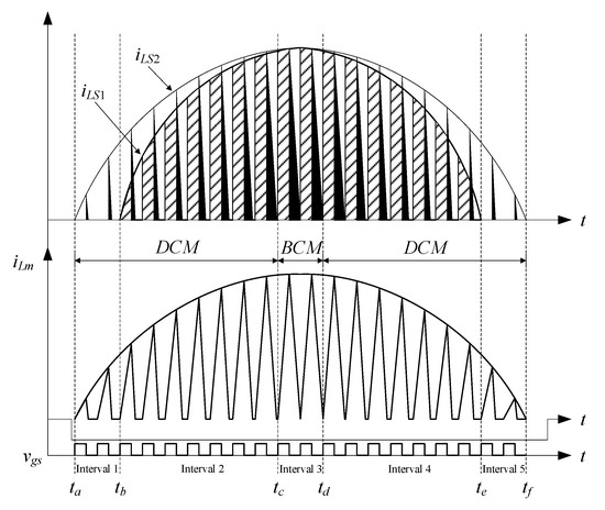
Figure 10.
Relationship between the magnetizing inductance current iLm and the LED string currents iLS1 and iLS2.
It can be seen from Figure 10 that both intervals 1 and 2 belong to DCM, but in interval 1 the LED string LS1 has not yet been turned on, and interval 3 belongs to BCM. The operating principles for the three intervals will be described as follows.
3.1. Operating Principle under Interval 1 in DCM
3.1.1. State 1: []
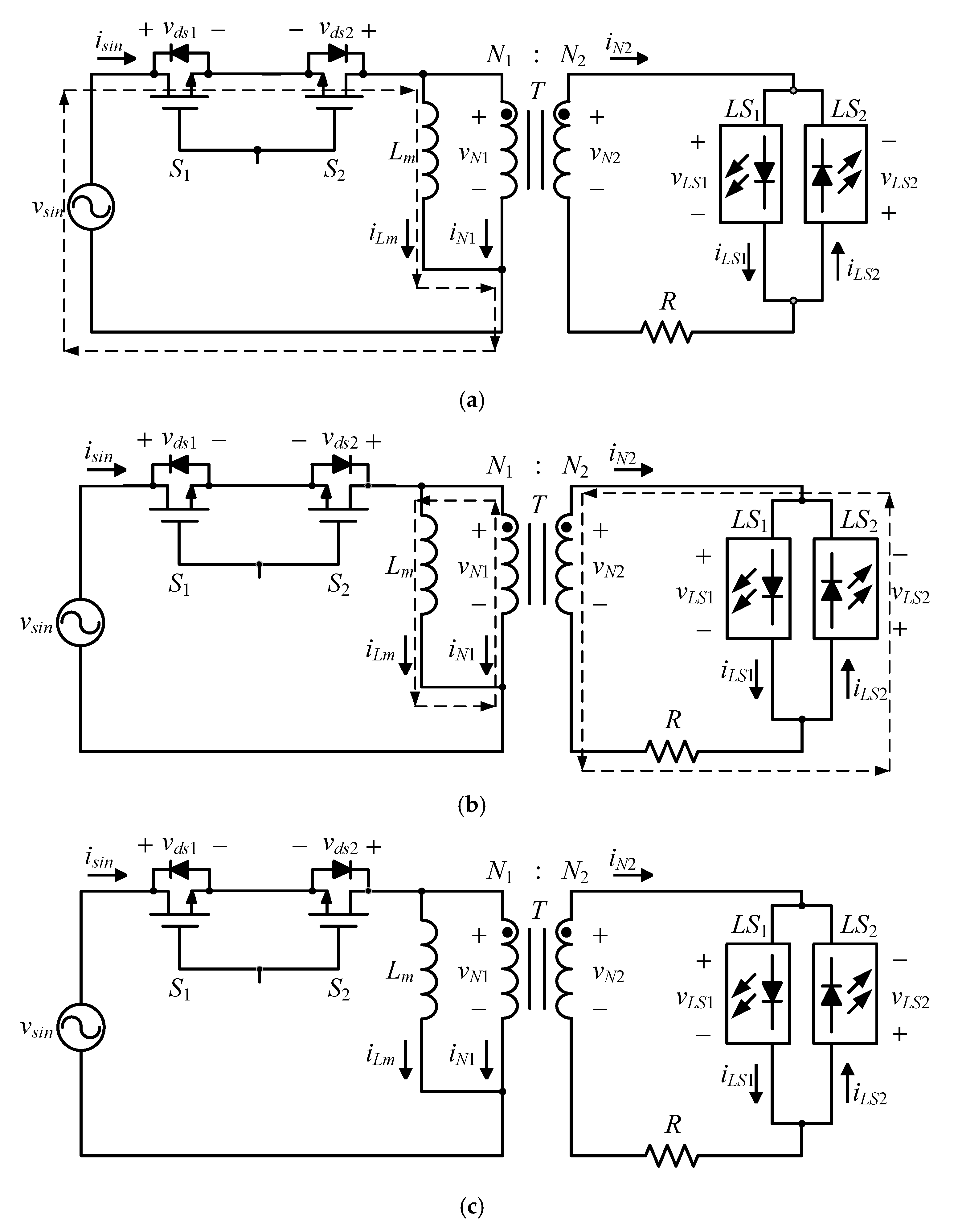
As shown in Figure 11a, when the main switches S1 and S2 are turned on, the secondary voltage vN2 is less than the forward conduction voltage VLS1 after the input voltage vsin is converted by the turns ratio of the coupled inductor T. Therefore, the LED string LS1 is not turned on, causing the coupled inductor T to store energy and hence not to perform energy transmission.

Figure 11.
Current flow under interval 1 for: (a) state 1; (b) state 2; (c) state 3.
3.1.2. State 2: []
As shown in Figure 11b, when the main switches S1 and S2 are turned off, the magnetizing inductor current iLm must continue to flow such that the LED string LS2 is conducted forward. During this state, the voltage across the magnetizing inducor Lm is negative, causing Lm to perform demagnetization.
3.1.3. State 3: []
As shown in Figure 11c, the magnetizing inductor current iLm is zero. Since the main switches S1 and S2 are still in the off-state, the circuit is opened until the main switches S1 and S2 are turned on and return to state 1. As the input voltage vsin is sufficient to turn on the LED string LS1, the operation enters interval 2.
3.2. Operating Principle under Interval 2 in DCM
3.2.1. State 1: []
As shown in Figure 12a, when the main switches S1 and S2 are turned on, the secondary voltage vN2 is greater than the forward conduction voltage VLS1 after the input voltage vsin is converted by the turns ratio of the coupled inductor T. Therefore, the LED string LS1 is turned on, and hence the coupled inductor T not only stores energy but also transfers energy to LS1. As the main switches S1 and S2 are turned off, the operation enters the next state.
Figure 12.
Current flow under interval 2 for: (a) state 1; (b) state 2; (c) state 3.
3.2.2. State 2: []
As shown in Figure 12b, the current flow of the circuit is the same as that in state 2 under interval 1.
3.2.3. State 3: []
As shown in Figure 12c, the current flow of the circuit is the same as that in state 2 under interval 1. As the input voltage vsin reaches the peak value, the operation enters interval 3.
3.3. Operating Principle under Interval 3 in BCM
3.3.1. State 1: []
As shown in Figure 13a, the input voltage vsin in this interval is the peak voltage vsin,max, so the circuit behavior changes from DCM to BCM. When the input voltage vsin reaches the peak voltage vsin,max, the main switches S1 and S2 are turned on to enter state 1. The current flow of the circuit is the same as that in state 1 under interval 2. Once the main switches S1 and S2 are turned off, the operation enters the next state.
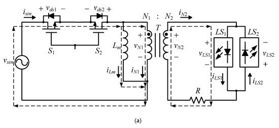

Figure 13.
Current flow under interval 3 for: (a) state 1; (b) state 2.
3.3.2. State 2: []
As shown in Figure 13b, the current flow of the circuit is the same as that in state 2 of interval 2. When the input voltage drops from the peak voltage vsin,max, the circuit behavior changes from BCM to DCM, and then the operation enters interval 4. The operation principle of interval 4 is the same as that of interval 2, so it will not be re-described herein again.
4. Design Considerations
Table 1 shows the system specifications. As for the used high-brightness white LED, it is manufactured by LENOO Electronics Co., New Taipei, Taiwan, with the product name of THEM-CLCX, and Table 2 displays its specifications. The number of LEDs is 20 and divided into 2 strings, which are connected in reverse parallel as the load of the AC LED driver.

Table 1.
System specifications.
Table 2.
Specifications for high-brightness white LED.
Before the key parameters of the circuit are determined, some symbols are defined as shown in Table 3.
Table 3.
Symbol definition.
4.1. Design of R
Since the circuit operating in BCM is at the voltage vsin,max, based on the following equations, the currents iLS1,pk and iL2,pk can be expressed to be
Since the two LED strings LS1 and LS2 are constructed by individual numbers of ten LEDs, the voltage VLS1 (=VSL2) is set to 35 V according to Table 2. The turns ratio n is chosen to be 4 to reduce the additional power dissipation on R. Therefore, based on (1), the value of R can be obtained to be 8 Ω.
4.2. Design of Lm
Based on (2), the value of D at the voltage vsin,max is 0.4868. In addition, based on (2), the value of Lm can be obtained to be 6.1 mH.
5. Experimental Results
In the following, some measurements contain waveforms, harmonic distribution, total harmonic distortion (THD), power factor (PF) and efficiency. It is noted that the scale on the x-axis for the last three figures is from high to low. In addition, as shown in Figure 14, the traditional AC LED driver, based on the circuit [13], has a line-frequency transformer inserted between the EMI filter and MOSFET switches, and is used as a comparison.
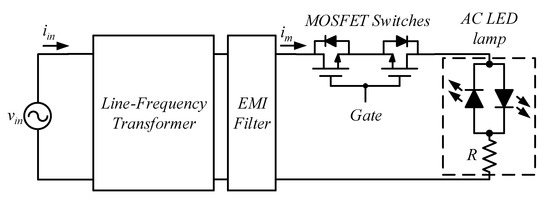
Figure 14.
Traditional AC LED driver based on a line-frequency transformer.
5.1. Measured Waveforms
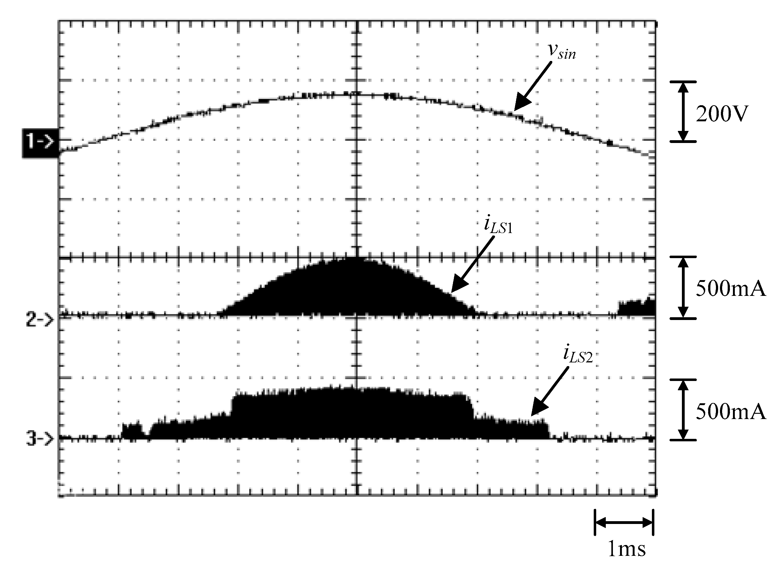
Figure 15, Figure 16, Figure 17, Figure 18 and Figure 19 show the measurement waveforms under 100% dimming command. Figure 15 shows the waveforms for the input voltage vsin and the input current isin. Figure 16 shows the waveforms over a positive half-cycle, including the AC input voltage vsin, the first LED string current iLS1 and the second LED string current iLS2. Figure 17 shows the waveforms at the peak voltage of vsin for a positive half-cycle, including the gate driving signals vgs1 and vgs2 for the main switches S1 and S2, respectively, and the first LED string current iLS1 and the second LED string current iLS2. Figure 18 shows the waveforms over a negative half-cycle, including the AC input voltage vsin, the first LED string current iLS1 and the second LED string current iLS2. Figure 19 shows the waveforms at the peak voltage of vsin for a negative half-cycle, including the gate driving signals vgs1 and vgs2 for the main switches S1 and S2, respectively, and the first LED string current iLS1 and the second LED string current iLS2.
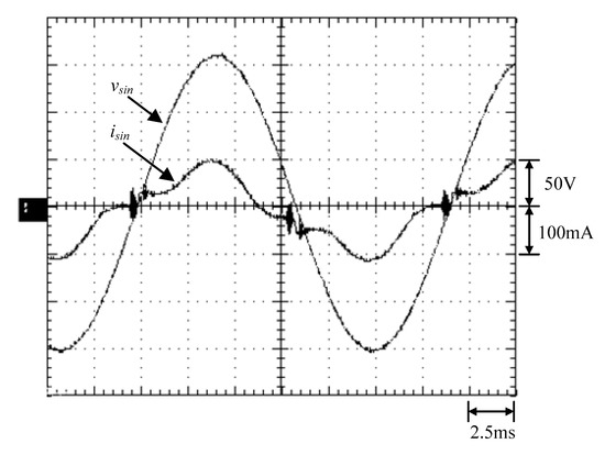
Figure 15.
Waveforms relevant to the input: (1) vsin; (2) isin.

Figure 16.
Waveforms at rated dimming command over a positive half-cycle: (1) vsin; (2) iLS1; (3) iLS2.
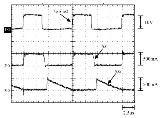
Figure 17.
Zoom-in Waveforms at the peak voltage of vsin: (1) vgs1, vgs2; (2) iLS1; (3) iLS2.
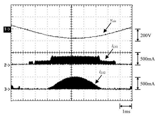
Figure 18.
Waveforms at rated dimming command over a negative half-cycle: (1) vsin; (2) iLS1; (3) iLS2.
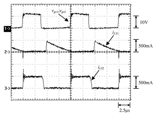
Figure 19.
Zoon-in waveforms at the peak value of vsin: (1) vgs1, vgs2; (2) iLS1; (3) iLS2.
From Figure 15, it can be seen that the values of THD and PF can be obtained to be 13.6% and 0.88, respectively. Figure 17 and Figure 19 show the currents iLS1 and iLS2, which have high-frequency oscillating currents at the moment when the main switches S1 and S2 are turned on. This is due to the resonance between the leakage inductance of the coupled inductor and the parasitic equivalent capacitance of the LED strings.
5.2. Harmonic Distribution
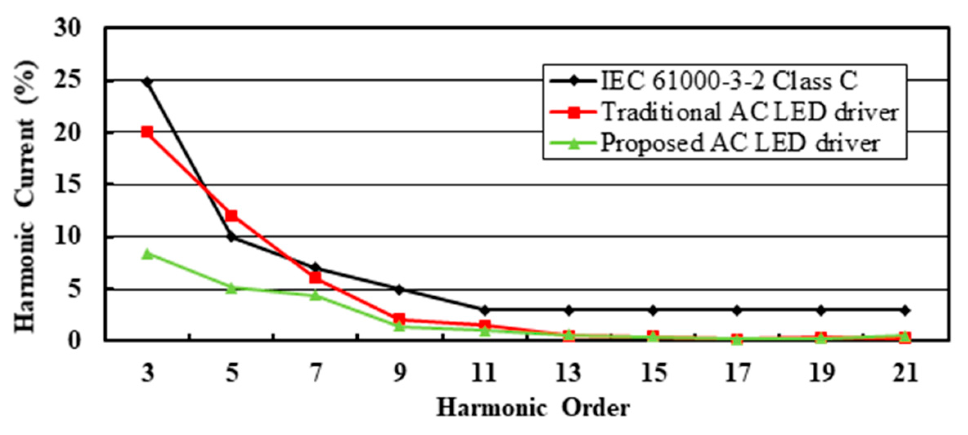
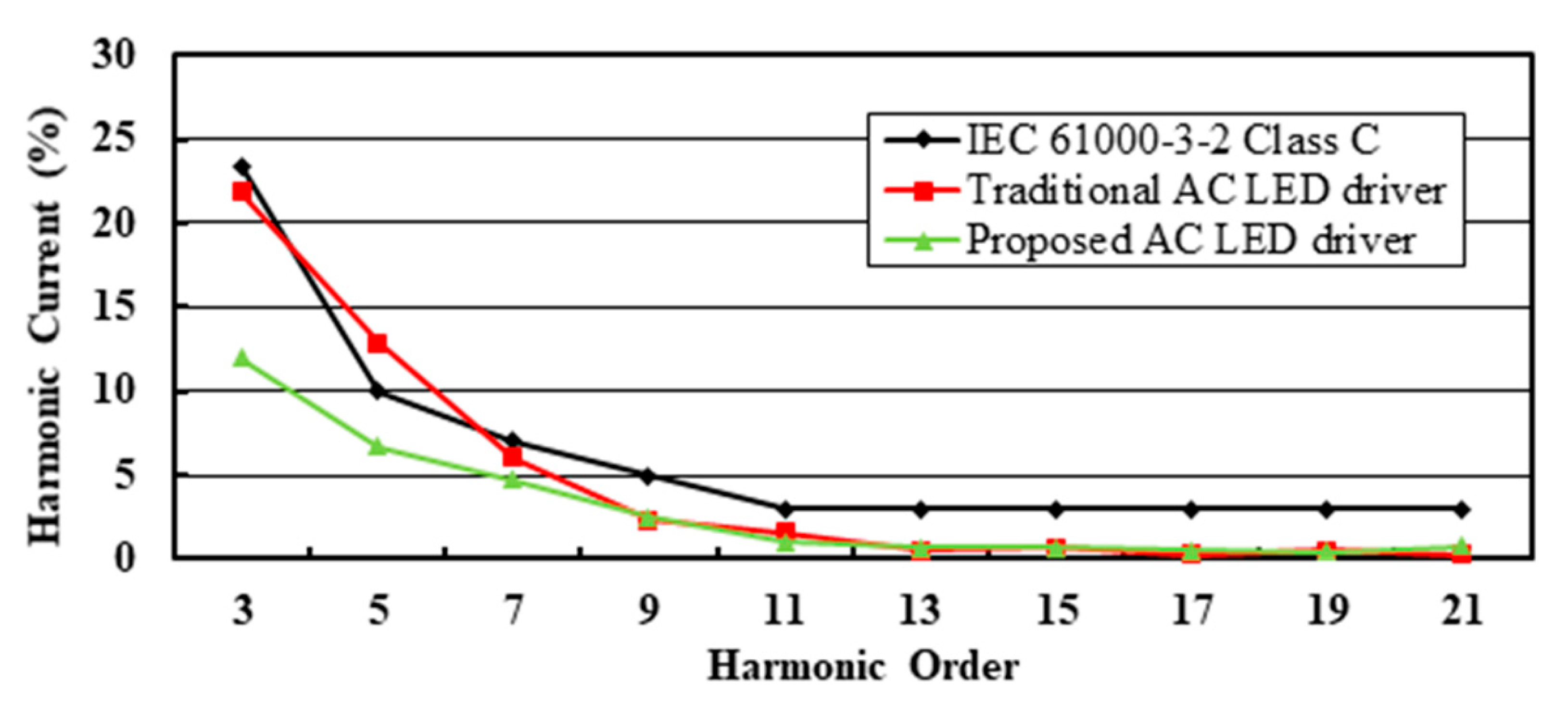
Figure 20, Figure 21 and Figure 22 show the harmonic distributions of the input currents under 100%, 50% and 20% of the rated dimming command, respectively. From these figures, it can be seen that for the proposed circuit, the harmonic distributions for any dimming command correspond to IEC 61000-3-2 Class C standard requirements, but the traditional circuit does not. In addition, the more the dimming command is, the lower is the value of the third harmonic.
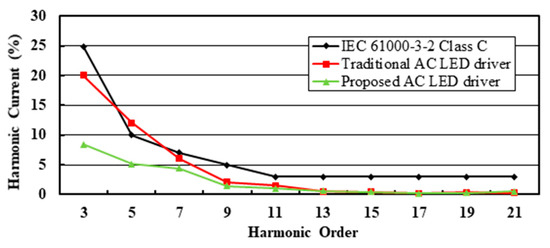
Figure 20.
Harmonic distribution under 100% dimming command.

Figure 21.
Harmonic distribution under 50% dimming command.
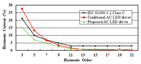
Figure 22.
Harmonic distribution under 20% dimming command.
Figure 20, Figure 21 and Figure 22 show the harmonic distributions of the input currents under 100%, 50% and 20% of the rated dimming command, respectively. From these figures, it can be seen that for the proposed circuit, the harmonic distributions for any dimming command correspond to IEC 61000-3-2 Class C standard requirements, but the traditional circuit does not. In addition, the more the dimming command is, the lower is the value of the third harmonic.
5.3. Total Harmonic Distortion (THD)
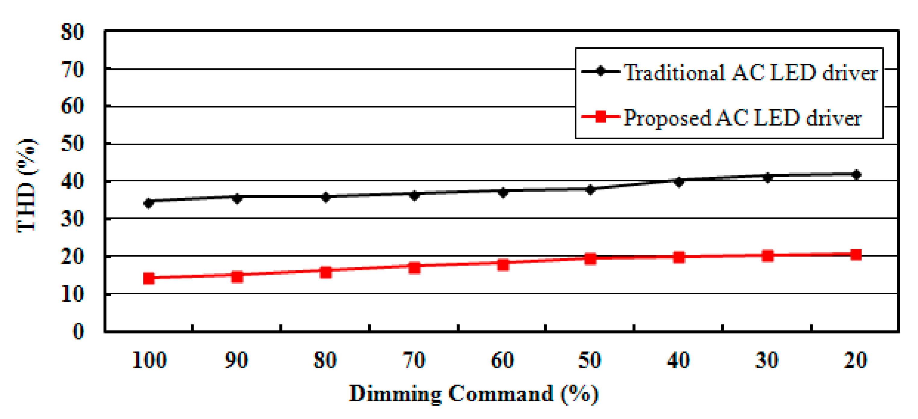
Figure 23 shows the curves of THD versus dimming command for the traditional and the proposed. From Figure 23, it can be seen that the THD of the proposed is significantly lower than that of the traditional, and the corresponding difference in THD between the two is up to about 20%.
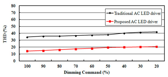
Figure 23.
Comparison in THD between the traditional and the proposed.
5.4. Power Factor (PF)
Figure 24 shows the curves of PF versus dimming command for the traditional and the proposed. From Figure 24, it can be seen that above 70% dimming command, the PF of the proposed is higher than that of the traditional and the corresponding difference in PF between the two is up to about 0.05, whereas below 70% dimming command, the PF of the proposed is lower than that of the traditional and the corresponding difference in PF between the two is up to about 0.14.
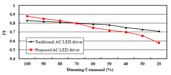
Figure 24.
Comparison in PF between the traditional and the proposed.
5.5. Efficiency
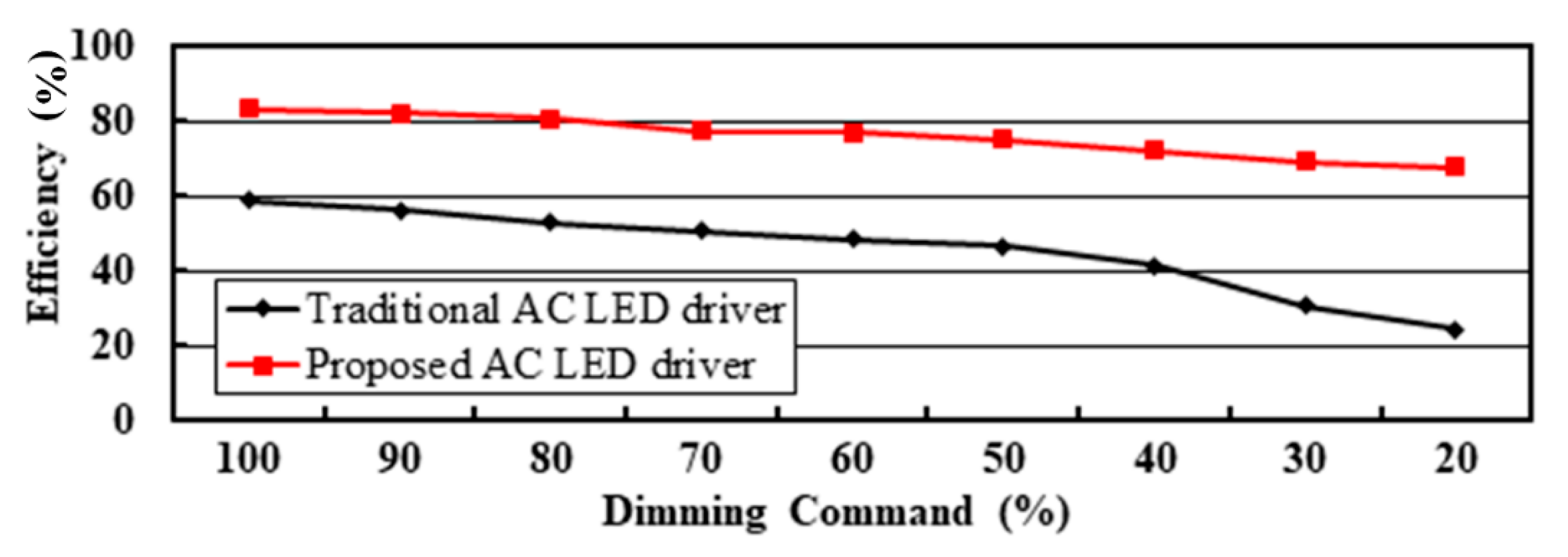
Figure 25 shows the curves of efficiency versus dimming command for the traditional and the proposed. From Figure 20, it can be seen that the efficiency of the proposed is significantly higher than that of the traditional and the corresponding difference in efficiency between the two is up to about 40%.
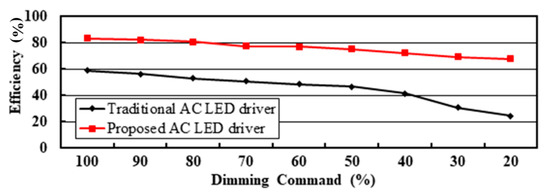
Figure 25.
Comparison in THD between the traditional and the proposed.
5.6. Experimenmtal Setup Photo
Figure 26 shows a photo of the experimental setup, including EMI filter, MOSFET, coupled inductor, current feedback circuit, FPGA, AC LED module.
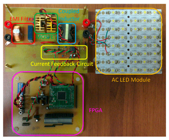
Figure 26.
Photo of the experimental setup.
6. Conclusions
The proposed AC LED driver has several advantages described as follows:
- (1)
- This AC LED driver belongs to a single-stage bridgeless rectifier;
- (2)
- There is no output electrolytic capacitor;
- (3)
- Since a coupled inductor is inserted between the bidirectional switch and the LED module, galvanic isolation can be achieved;
- (4)
- Since the turns ratio of the coupled inductor can be adjusted, the number of LEDs per LED string can be flexibly designed;
- (5)
- Since the coupled inductor has transformer behavior, during the turn-on period of the bidirectional switch the coupled inductor can transfer the energy to one LED string and store the energy in the magnetizing inductor simultaneously;
- (6)
- Since the coupled inductor has also inductor behavior, during the turn-off period of the bidirectional switch, the magnetizing inductor can release the energy to the other LED string; and
- (7)
- As for LED dimming, it can be realized by directly tuning the control signal for the bidirectional switch, without any dimming circuit.
Author Contributions
Conceptualization, Y.-T.Y. and K.-I.H.; methodology, Y.-T.Y.; software, C.-W.W.; validation, Y.-T.Y., K.-I.H., and C.-W.W.; formal analysis, Y.-T.Y.; investigation, C.-W.W.; resources, Y.-T.Y.; data curation, C.-W.W.; writing—original draft preparation, K.-I.H.; writing—review and editing, K.-I.H.; visualization, C.-W.W.; supervision, K.-I.H.; project administration, K.-I.H.; funding acquisition, Y.-T.Y. All authors have read and agreed to the published version of the manuscript.
Funding
This research was funded by the Ministry of Science and Technology, Taiwan, under the Grant Number: MOST 109-2222-E-167-003-MY3.
Data Availability Statement
No new data were created or analyzed in this study. Data sharing is not applicable to this article.
Conflicts of Interest
The authors declare no conflict of interest.
References
- Castro, I.; Vazquez, A.; Arias, M.; Diego, G.; Lamar, H.; Marta, M.; Sebastian, J. A review on flicker-free AC–DC LED drivers for single-phase and three-phase AC power grids. IEEE Trans. Power Electron. 2019, 34, 10035–10057. [Google Scholar] [CrossRef]
- Liu, S.; Wu, X.; Yuan, F.; Zhao, M. An adaptive on-time controlled boost LED driver with high dimming ratio. In Proceedings of the 38th Annual Conference on IEEE Industrial Electronics Society (IECON), Montreal, OC, Canada, 25–28 October 2012; pp. 210–214. [Google Scholar]
- Huang, C.-H.; Wu, H.-H.; Wei, C.-L. Compensator-free mixed-ripple adaptive on-time controlled boost converter. IEEE J. Solid-State Circuits 2018, 53, 596–604. [Google Scholar] [CrossRef]
- Hong, W.; Jeong, H.; Lee, M. A 10-MHz current-mode constant on-time boost converter with a translinear loop-based current sensor. In Proceedings of the 9th International Conference on Modern Circuits and Systems Technologies (MOCAST), Bremen, Germany, 7–9 September 2020; pp. 1–4. [Google Scholar]
- Wu, H.; Zhang, Y.; Zhao, M.; Shen, H.; Wu, X. A constant-on-time based buck controller with active PFC for universal input LED system. In Proceedings of the IEEE 11th International Conference on Power Electronics and Drive Systems, Sydney, NSW, Australia, 9–12 June 2015; pp. 551–556. [Google Scholar]
- Yun, D.; Kim, H.; Baek, D.; Cho, S.; Yoon, J.; Lee, J. A fixed-frequency synchronous boost converter based on adaptive on-time control with a new reverse phase ripple injection compensation. In Proceedings of the IEEE Energy Conversion Congress and Exposition (ECCE), Detroit, MI, USA, 11–15 October 2020; pp. 2244–2250. [Google Scholar]
- Hwu, K.I.; Tu, W.C.; Hong, M.J. A dimmable LED driver based on current balancing transformer with magnetizing energy recycling considered. IEEE/OSA J. Disp. Technol. 2014, 10, 388–395. [Google Scholar] [CrossRef]
- Hwu, K.I.; Tu, W.C.; Fang, Y.T. Dimmable AC LED driver with efficiency improved based on switched LED module. IEEE/OSA J. Disp. Technol. 2014, 10, 171–181. [Google Scholar] [CrossRef]
- Hwu, K.I.; Tu, W.C. Controllable and dimmable AC LED driver based on FPGA to achieve high PF and low THD. IEEE Trans. Ind. Inform. 2013, 9, 1330–1342. [Google Scholar] [CrossRef]
- Hwu, K.I.; Shieh, J.-J. Dimmable AC LED driver based on series drive. IEEE/OSA J. Disp. Technol. 2016, 12, 1097–1105. [Google Scholar] [CrossRef]
- Ren, N.; Lyu, X.; Cao, D.; Zuo, Z.; Li, R. High-efficiency multiple-string linear LED driver with genetic algorithm for low power application. In Proceedings of the IEEE Energy Conversion Congress and Exposition (ECCE), Portland, OR, USA, 23–27 September 2018; pp. 4717–4720. [Google Scholar]
- Chen, Y.; Zhong, D.; Nan, Y. An input-adaptive multi-segmented LED driver for wide AC input applications. In Proceedings of the IEEE Energy Conversion Congress and Exposition (ECCE), Portland, OR, USA, 23–27 September 2018; pp. 4728–4732. [Google Scholar]
- Jung, H.; Kim, J.; Lee, B.; Yoo, D. A new PWM dimmer using two active switches for AC LED lamp. In Proceedings of the 2010 International Power Electronics Conference-ECCE ASIA, Sapporo, Japan, 21–24 June 2010; pp. 1547–1551. [Google Scholar]


Publisher’s Note: MDPI stays neutral with regard to jurisdictional claims in published maps and institutional affiliations. |
© 2021 by the authors. Licensee MDPI, Basel, Switzerland. This article is an open access article distributed under the terms and conditions of the Creative Commons Attribution (CC BY) license (https://creativecommons.org/licenses/by/4.0/).