Abstract
With the advent of 5G, artificial intelligence (AI), Internet of Things (IoT), cloud computing, Internet plus, and so on, data traffic is exploding and higher requirements are put forward for information transmission and switching. Traditional switching requires optical/electrical/optical conversions, which brings additional power consumption and requires the deployment of large amounts of cooling equipment. This increases the cost and complexity of the system. Moreover, limited by the electronic bottleneck, electrical switching will suffer from many problems such as bandwidth, delay, crosstalk, and so on, with the continuous reduction in device footprint. Optical switching does not require optical/electrical/optical conversions and has lower power consumption, larger capacity, and lower cost. Silicon photonic switches received much attention because of their compatibility with the complementary metal-oxide-semiconductor (CMOS) process and are anticipated to be potential candidates to replace electrical switches in many applications such as data center and telecommunication networks. 2 × 2 silicon photonic switches are the basic components to build the large-scale optical switching matrices. Thus, this review article mainly focuses on the principle and state of the art of 2 × 2 silicon photonic switches, including electro-optic switches, thermo-optic switches, and nonvolatile silicon photonic switches assisted by phase-change materials.
1. Introduction
Today, the Internet of everything brought about an explosion of traffic. Traditional integrated circuits are required to have larger bandwidth and higher rate to transmit, process, and store huge amounts of data. However, with the continuous reduction in transistor size, traditional electrical interconnection technology encountered a series of bottlenecks in terms of speed, bandwidth, and power consumption, etc., which seriously restricts the development of integrated circuits [1]. Additionally, the shrinking size of transistors also makes manufacturing more difficult and costly. Compared with electrons, photons have natural advantages as information carriers. Optical communication, with its advantages of low signal loss, large transmission capacity, and anti-electromagnetic interference [1], not only exhibits great advantages in long-haul communication fields such as metropolitan area networks (MAN) and long-distance backbone networks, but also gradually infiltrates into short-haul communication fields such as servers and computer racks in recent years. Optical communication technology is undergoing the development process from long-distance communication to short-distance communication and progressively to on-chip optical communication. Photonic integrated circuits (PICs) made tremendous progress over the last few decades and exhibited advantages over electronics in information transmission with its small footprints, high-speed operation, low power consumption, and low-cost packaging. With the development of fabrication process, large-scale PICs were reported [2,3,4]. In contrast with application-specific PICs (ASPICs), which are designed to implement specific functions, recent advances in silicon photonics desire urgently programmable and generic PICs [5,6,7,8] to satisfy a wide range of applications, including light detection and ranging [9], microwave photonics [5,6], optical neural networks [4], and quantum information [3,10,11]. Like the field-programmable gate arrays (FPGAs) in electronics, programmable PICs have far higher flexibility and adaptability, which can effectively reduce the cost and complexity of the system. 2 × 2 optical switches are the fundamental and critical building blocks to constitute programmable PICs, which can be used to implement optical signal routing and switching. High-performance optical switches are desired to reach the system demands.
For the last few decades, various types of optical switches were deeply researched; including microelectromechanical systems (MEMS)-based optical switches [12], semiconductor optical amplifier (SOA) switches [13], liquid crystal optical switches [14], photonic crystal all-optical switches [15]. Compared with these, silicon photonic switches attracted extensive attention for its unique characteristics such as high-density integration, good compatibility with the mature complementary metal-oxide-semiconductor (CMOS) process, and strong plasma dispersion and thermo-optic effects. Furthermore, phase-change materials (PCMs) were introduced in silicon photonic switches to realize nonvolatile optical switches. Some review articles were reported on the silicon photonic switches [16,17,18,19,20]. Nevertheless, 2 × 2 silicon photonic switches as the basic block to build programmable PICs were not systematically reviewed yet. In this paper, we will discuss the 2 × 2 silicon photonic switches from the view of operating principle and state of the art, including not only the traditional silicon electro-optic and thermo-optic switches, but also the new nonvolatile silicon photonic switches assisted by PCMs sprung up in the last few years.
2. 2 × 2 Silicon Electro-Optic Switches
2.1. Principle
The electro-optic effects in silicon mainly include plasma dispersion effect, Kerr effect, Franz–Keldysh (F-K) effect, and quantum confined Stark effect (QCSE) [1]. Because the Kerr effect and F-K effect in bulk silicon are very weak, high-speed silicon electro-optic switches mainly utilize the plasma dispersion effect. Plasma dispersion effect is an indirect electro-optic effect. Under the applied electric field, the refractive index and absorption coefficient will change due to the change of free carrier concentration in the active region. This will change the phase and amplitude of light, so as to realize electro-optic modulation. The change of refractive index and absorption coefficient caused by the change of free carrier concentration in silicon at the wavelength of 1550 nm has the following empirical formula [1,21]:
In the formula, ΔNe and ΔNh are the varying concentration of electrons and holes, Δne and Δnh are the changes of refractive index induced by the changes of free electron and hole concentration, Δαe and Δαh are the changes of absorption coefficients, respectively. Correspondingly, at the wavelength of 1310 nm [1,21]:
The change of refractive index caused by the change of free carrier concentration can be estimated conveniently using the above formula. However, the change of refractive index is always accompanied by the absorption of light by free carriers.
There are commonly three modulation mechanisms to manipulate electrically the free carrier concentration in plasma-dispersion-based silicon electro-optic devices: carrier injection, carrier accumulation, and carrier depletion, as shown in Figure 1 [22]. The electrical structure of a carrier-accumulation electro-optic device is a capacitor which is formed by a thin silica (SiO2) insulating layer embedded in silicon ridge waveguide. The two surfaces of the capacitor accumulate positive and negative charges, respectively, with an applied electric field. The change of the free carrier concentration leads to the change of the effective refractive index of the mode in the waveguide. The speed of the carrier-accumulation electro-optic device is usually limited by the resistance and capacitance. The electrical structure of a carrier-injection electro-optic device is a pin junction. Highly doped p-region and n-region are separated by an intrinsic region. The free carrier concentration of the intrinsic region changes with forward bias voltage, which makes the effective refractive index change. The carrier-injection electro-optic device has a simple and compact structure and high modulation efficiency, but its speed is limited by the diffusion time of carriers. The electrical structure of pin junction was used in switch design for a long time [23]. The electrical structure of a carrier-depletion electro-optic device is a pn junction working in reverse bias voltage. The depletion area of the pn junction becomes larger as the reverse bias voltage increases, which will change the free carrier concentration and then modulate the refractive index. The carrier-depletion electro-optic device is usually fast, which is the main way to realize the high-speed MZI electro-optic device, but its loss is also high. For silicon electro-optic switch applications, the electrical structure of the phase shifter mostly adopts a pin junction operated in carrier-injection mode.
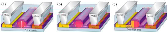
Figure 1.
Typical structures of the phase shift arm that implement the three modulation mechanisms in silicon electro-optic switches based on plasma dispersion effect [22]. (a) Carrier accumulation, (b) carrier injection, (c) carrier depletion.
2.2. State of the Art
The research on silicon electro-optic switches was first started in the mid-1980s. R. A. Soref and J. P. Lorenzo proposed 2 × 2 silicon electro-optic switches working at 1.3 μm and 1.6 μm wavelengths [23,24]. The two basic structures of 2 × 2 silicon photonic switches are Mach–Zehnder interferometer (MZI) and microring resonator (MRR). MRR optical switches have wavelength selectivity, and because the resonant characteristic can enhance the phase, MRR optical switches generally have smaller size and lower power consumption than MZI switches [25]. However, MRR optical switches are not widely used for the following two reasons. Firstly, the optical bandwidth of MRR switches is limited. Secondly, they are sensitive to fabrication errors, temperature, and laser wavelength drift, which makes wavelength alignment and stabilization challenged. The 2 × 2 MZI silicon electro-optic switch is an early researched electro-optic switch. It is favored by many researchers for its good anti-interference ability, large working bandwidth, and nanosecond scale switching speed. Many universities and research institutions internationally reported on it. As previously mentioned, the modulation of refractive index is always accompanied by the absorption of light by free carriers, which will result in the unbalanced power distribution of the two phase shift arms. Thus, the MZI-based silicon electro-optic switches usually have large crosstalk (CT).
To address this problem, Wang et al. reduced the CT to −24.5 dB and −40 dB by using integrated attenuator and two cascaded Mach–Zehnder (MZ) structures, respectively [26]. Xing et al. reported a low crosstalk 2 × 2 silicon electro-optic switch with a double-gate configuration [27], reducing the CT to −31 dB. However, this approach increases the footprint and power consumption of the switch, and the insertion loss (IL) is also as high as 9 dB. To reduce the power consumption, Dong et al. reduced the π-phase switching power consumption to 0.6 mW by extending the phase shift arm [28]. The switching time is 6 ns and the CT is lower than −17 dB for a bandwidth of 60 nm. Lu et al. experimentally demonstrated a 2 × 2 silicon electro-optic switch based on a dual-ring assisted Mach–Zehnder interferometer (DR-MZI) [29]. The thermo-optic power consumption for correcting phase error is 2.31 mW and the electro-optic switching power is 0.69 mW. The IL and CT of the switch are within 1.8 dB to 3.4 dB and better than −20 dB, respectively. The rise and fall times are about 0.41 ns. To further optimize the IL, CT, and power consumption, Dupuis et al. demonstrated a low-loss and low-crosstalk 2 × 2 MZI silicon photonic switch in the O-band by adopting a push-pull drive mode [30]. The measured IL and CT are 1.2 dB and −27 dB, respectively. The average power consumption is 1 mW with a transition time of ~4 ns. By introducing a new modulation scheme of push-pull modulation with a pre-biased π/2 phase shift, Xing et al. reported an MZI-based electro-optic switch with both a low CT and a compact footprint [31]. With 200 μm-long phase shift arms, the CT is less than −20 dB in the 20 nm wavelength range around 1530 nm and the measured IL is about 3 dB for both states. The rise and fall times are 5.32 ns and 5.41 ns, respectively. Subsequently, Dupuis et al. proposed an optical switch with an MZI phase shifter embedded in one arm and an adjustable attenuator integrated in the other arm to remain the power balance of the two arms [32], thus reducing the CT to −34.5 dB. While the IL of the switch is about 2 dB at the wavelength of 1310 nm, the power consumption and switching time are 2 mW and 4 ns, respectively. Dehghani et al. proposed a 2 × 2 high-performance dual-shaped MRR-based optical switch [33]. The main advantage of the switch is the removal of waveguide crossing resulting in lower crosstalk. The CT is −15 dB for the through port and lower than −20 dB for the drop port. The ILs for through and drop states are 0.8 dB and 1.3 dB at λ = 1462.2 nm and λ = 1501 nm, respectively. Sun et al. demonstrated two typical silicon electro-optic switches based on coupled microring resonator (CMRR) and MZI structures, as illustrated in Figure 2 [34]. The measured ILs of the CMRR-based switch are less than 1 dB at the drop port and less than 2.5 dB at the through port. The CTs are about −19.5 dB and −10.8 dB at the through and drop ports, respectively. The OFF-ON switchover power is 10.9 mW. The rise time and fall time are 11.9 ns and 12.3 ns. The MZI-based switch worked at a push-pull configuration by introducing a π/2 phase bias (Figure 2c). This needs less phase shift, which leads to lower power consumption. Then, less loss and crosstalk can be attained. The measured ILs are less than 1 dB at the bar port and less than 2 dB at the cross port. The CTs are about −22.8 dB and −15.6 dB at the cross port and bar port, respectively. The OFF-ON switchover power is 15.0 mW. The rise time and fall time are 11.7 ns and 12.6 ns, respectively. A broadband silicon photonic switch is desired for wavelength-division multiplexing (WDM) applications on photonic networks on chip. Campenhout et al. demonstrated a 2 × 2 silicon electro-optic switch with large-bandwidth [35]. Because the 3 dB couplers were improved by cascaded two wavelength insensitive directional couplers, it broke through the limited bandwidth of traditional optical switches. A 110 nm bandwidth is achieved. The CT and switching time are −17 dB and 4 ns, respectively. The power consumption of the switch is 3.1 mW and the VπL is as low as 0.06 V·mm. Calò et al. expanded the bandwidth of an MZI switch to 115 nm by adopting three-waveguide (3W) interference structure [36].
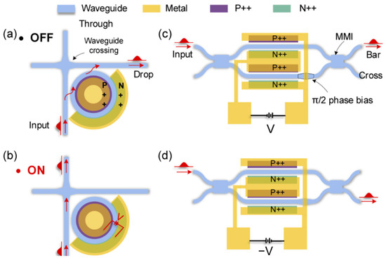
Figure 2.
Operating mechanism of (a,b) coupled microring resonator (CMRR)-based and (c,d) Mach–Zehnder interferometer (MZI)-based silicon electro-optic switches at the (a,c) OFF state and (b,d) ON state. Reprinted with permission from ref. [34] © The Optical Society.
3. 2 × 2 Silicon Thermo-Optic Switches
3.1. Principle
Silicon thermo-optic switches are based on the thermo-optic effect of silicon material. The thermo-optic effect is a physical effect that the optical properties of materials change with temperature, thus inducing the change of the phase when the light propagates in the materials. The change of refractive index with temperature can be expressed as
In the formula, n0 is the refractive index of the material, ΔT is the change in temperature, α is the thermo-optic coefficient that is related to material. At the temperature of 300 K~550 K and wavelength of 1523 nm, the empirical formula of the thermo-optic coefficient of silicon with temperature is as follows [37]:
According to the formula, the thermo-optic coefficient of silicon is about 1.85 × 10⁻⁴ K−1 at the temperature of 300 K, which is one order of magnitude larger than that of SiO2. Hence, the silicon thermo-optic switch has higher efficiency than that based on the thermo-optic effect of SiO2. Moreover, silicon has a high thermal conductivity of 1.49 W/(cm·K), which makes the silicon thermo-optic switch have fast switching speed. The switching time of the silicon thermo-optic switch is generally in the order of microseconds. In addition, the thermal conductivity of SiO2 buried layer in silicon-on-insulator (SOI) is very small, only 1/100 of that of silicon, which can play a good insulation role and reduce heat dissipation, thus reducing the switching power consumption.
The structures of 2 × 2 silicon thermo-optic switches are mostly MZI, which consists of two 3 dB couplers and two phase shift arms, as shown in Figure 3. The commonly used 3 dB couplers in 2 × 2 MZI silicon photonic switches are directional couplers (DCs) and multimode interferometers (MMIs). DCs usually have low loss, and their power distribution ratio can be controlled easily. MMIs usually have high loss and a large footprint, but they are insensitive to polarization and fabrication errors, and they support large bandwidth. Without heating, the temperature of the two phase shifters is the same. The two beams through 3 dB couplers destructive interference at the bar port and constructive interference at the cross port, the signal outputs through the cross port. If one of the phase shifters is heated so that the optical signal passing through it has a phase shift of π, the input signal will constructive interference at the bar port and destructive interference at the cross port, and it will output from the bar port. Therefore, the ON/OFF state of a silicon thermo-optic switch can be switched by heating the silicon.
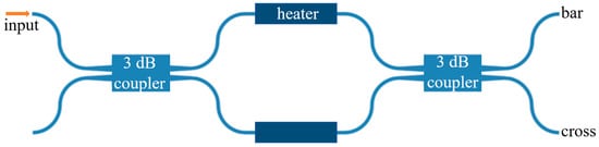
Figure 3.
Schematic illustration of the 2 × 2 MZI silicon thermo-optic switches.
3.2. State of the Art
There are various types of heaters in silicon thermo-optic devices. Metallic heaters are the commonly used one. To avoid the metal absorption, a thick SiO2 upper cladding usually more than 1 μm is needed, which will lead to low heating efficiency and low switching speed [38]. To reduce the power consumption of a silicon thermo-optic switch, an integrated silicon heater formed by highly doped silicon waveguides was proposed to achieve high-speed and low-power thermal tuning [39,40]. Nevertheless, the process to fabricate the heater with different doping levels are usually complicated and hard to control. Graphene heaters are another type of heaters used in silicon thermo-optic devices to improve heating efficiency and response speed. In 2014, a graphene heater on SOI nanowires was reported for the first time [41], and then, it was used to realize a silicon thermo-optic switch [42]. Adopting undercut structures is also an effective way to reduce the power consumption of the silicon thermo-optic devices [43,44]. In 2019, Chen et al. proposed a MZI silicon thermo-optic switch, and a laterally supported suspended phase arm and two metallization steps are used to lower the switching power [45]. The measured results show that the power consumption of the switch is 1.1 mW, the rise and fall times are 76 μs and 48 μs, respectively. A broadband DC with 100 nm bandwidth in the wavelength range of 1500 nm~1600 nm was used as a 3 dB power splitter. The overall footprint of the device is 240 μm × 24 μm, the IL and extinction ratio (ER) are about 0.5 dB and 11.5 dB, respectively. The proposed structure offers a good trade-off between switching power and temporal response.
To further improve the figure of merit (FOM) defined as the product of power consumption and thermal time constant of the thermo-optic switch, Duan et al. proposed a 2 × 2 thermo-optic MZI switch with laterally supported suspended ridge waveguides as the phase shift arms and a metallic heater set on the slab of the ridge waveguide [46]. The power consumption of the switch is 1.07 mW. The IL and ER are about 0.5 dB and 30 dB at the wavelength of 1555 nm and IL is smaller than 0.5 dB in the wavelength range of 1540 nm~1565 nm. The rise time (tup) and fall time (tdown) are 10.4 μs and 5.2 μs, respectively. The thermal time constant, which is defined as tup/2.2, is about 4.7 μs. The FOM is one order magnitude smaller than that proposed in reference [47]. The switch has an overall footprint of 450 μm × 30 μm. The proposed 2 × 2 silicon thermo-optic switch may have a potential application for on-chip optical information processing and reconfigurable network. In 2021, Kita et al. reported a 2 × 2 ultrafast MZI silicon thermo-optic switch with periodic electrodes which worked in the C band [48]. The periodic electrodes can be used to decrease the electric resistance of the heater. By adopting an integrated heat sink and an asymmetric doped MZI structure, an ultrahigh-speed silicon thermo-optic switch was achieved. The rise time and fall time are 0.36 μs and 0.5 μs, respectively. The power consumption is 22.6 mW. The FOM is further decreased compared with that in reference [46]. The IL and ER of the device are about 1 dB and 41.7 dB, respectively. The footprint is 60 μm × 30 μm, which was significantly improved compared with the silicon thermo-optic switches mentioned above [45,46].
Due to the imperfection of the fabrication process, the actual sizes of the fabricated devices are usually deviated from that of the theoretically designed devices, which will introduce random phase errors in the MZI silicon photonic switches [49]. The random phase errors of each MZI silicon photonic switch have to be compensated in large-scale optical matrix switches, which will introduce extra power consumption and increase the complexity of the system [35,49,50]. Song et al. proposed a MZI silicon thermo-optic switch with low random phase errors by adopting widened and shortened phase shifters for the first time [51]. The random phase errors can be reduced to a third of those of the MZI optical switches with 450 nm single-mode phase shifters. The IL and ER of the device are about 1 dB and more than 30 dB in the wavelength range from 1530 nm to 1590 nm. The power consumption is 2.7 mW for the off-state and 30.6 mW for the switching from the off-state to the on-state. Several typical 2 × 2 silicon photonic switch units including electro-optic and thermo-optic switches are summarized and compared in Table 1.

Table 1.
Comparison of several typical 2 × 2 silicon photonic switches.
3.3. Multiplexing Schemes
With the ever-increasing data traffic, the demands on the communication capacity increased explosively [52]. To reach this requirement, several multiplexing schemes were exploited to expand the transmission capacity, including WDM, mode-division multiplexing (MDM), and polarization-division multiplexing (PDM). By utilizing multiple physical dimensions, an optical switch can be realized to achieve scaled capacity. In 2017, Jia et al. demonstrated a 2 × 2 multimode silicon thermo-optic switch compatible with WDM and MDM for photonic networks-on-chip [53]. The architecture of the switch is shown in Figure 4. The multimode optical switch can support four spatial modes and has a broad optical bandwidth. The inter-mode crosstalk for the same optical link is smaller than −22.1 dB and the link-crosstalk for all four modes is less than −18.8 dB. The total power consumptions are 117.9 mW and 116.2 mW in the cross and bar states, respectively. The power consumptions of each mode optical switch are listed in Table 2. The switching time is approximately 21 μs. Subsequently, Zhang et al. presented a 2 × 2 mode-polarization-wavelength selective switch (MPWSS) based on the MRRs and demonstrated a proof-of-concept experiment with eight channels consisting of two modes, two polarizations, one wavelength, and two input/output ports [54]. The demonstration paves the way for future multi-dimensional, large capacity, scalable, and low power optical switches. In 2021, Hang et al. proposed a 2 × 2 simultaneous three-mode thermo-optic switch, which consists of four ψ-junctions and three kinds of 2 × 2 MMI couplers [55]. The proposed multimode switch could operate in 40 nm optical bandwidth from 1520 nm to 1560 nm with IL and CT lower than 3 dB and −22 dB, respectively. The power consumption and switching time are under 40 mW and 4.4 μs, respectively. The footprint of the device is very compact with a small size of 12 μm × 1300 μm, providing great potentials for applications in WDM-MDM switching systems and large-scale integrated photonic circuits. MDM multimode optical switches offer important operational functions as they add flexibility and reconfigurability to MDM-based systems. Zhang et al. demonstrated an MZI-based energy efficient mode insensitive silicon thermo-optic switch [56]. To eliminate the mode dependence of the phase shifter tuning efficiency, an inverse-designed mode exchanger was introduced to maintain the exact same phase shift for the first two TE modes. The schematic of the mode insensitive silicon photonic switch and the corresponding mode multiplexer, demultiplexer, and the mode insensitive phase shifter is illustrated in Figure 5. The proposed device realized an exact mode insensitive switching. The power consumption is 25.6 mW with 7.9 mW for the cross state and 33.5 mW for the bar state. The average ILs, worst modal CTs, and ERs are 2.7 dB (2.1 dB), −16 dB (−15.5 dB), and 19.5 dB (23.7 dB) for the cross (bar) state for TE0 mode over a 40 nm optical bandwidth (1530 nm~1570 nm), respectively. Additionally, they are correspondingly 3.1 dB (2.8 dB), −14.1 dB (−14.5 dB), and 18.3 dB (23.4 dB) for the cross (bar) state for TE1 mode. Furthermore, the switch design can be scalable to higher order modes.
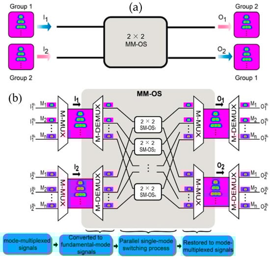
Figure 4.
(a) General scheme and (b) detailed architecture of the proposed 2 × 2 multimode silicon thermo-optic switch. MM-OS: multimode optical switch; SM-OS: single mode optical switch; M-MUX: mode multiplexer; M-DEMUX: mode demultiplexer. Reprinted with permission from ref. [53] © The Optical Society.
Table 2.
Power consumptions and driving voltages of the single mode silicon photonic switches. Reprinted with permission from ref. [53] © The Optical Society.
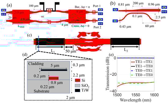
Figure 5.
Schematic illustration of (a) the mode insensitive silicon photonic switch and (b) the mode multiplexer and demultiplexer. (c) Schematic illustration and (d) cross-section of the mode insensitive phase shifter. (e) Simulated transmission spectrum of the mode exchanger (ME). Reprinted with permission from ref. [56] © The Optical Society.
4. 2 × 2 Nonvolatile Silicon Photonic Switches Assisted by PCMs
4.1. PCMs
Silicon electro-optic and thermo-optic switches have their own advantages in speed and crosstalk. However, the optical modulation based on the plasma dispersion effect and thermo-optic effect of silicon is weak (usually Δn < 0.01). This will result in a large footprint (usually hundreds of micrometers) and high-power consumption (several milliwatts). Furthermore, silicon electro-optic and thermo-optic switches require continuous external power to maintain their ON/OFF state, which leads to high static power consumption. PCMs can undergo rapid and reversible phase transitions triggered by external stimuli such as optical [57,58], electrical [59], or thermal [60,61] approaches. The optical properties of PCMs exhibit great differences between crystalline and amorphous states due to the difference of the atomic arrangement. The relationships between complex refractive index and wavelength of several PCMs are shown in Figure 6 [62,63]. The introduction of PCMs into the design of silicon photonic switches has many advantages. Firstly, there is a great difference in optical constants (Δn > 1) between crystalline and amorphous states of PCMs over a broad spectral region [64], which can realize strong optical modulation. Secondly, the crystalline and amorphous phases of PCMs can be stable for many years at temperature from 0 to 70 °C [65]. Therefore, no additional power is required to maintain the ON/OFF state of the switch. Thirdly, the phase transition speed can be on the order of nanosecond/sub-nanosecond [62,66]. Finally, the PCMs have good durability and scalability [67,68].
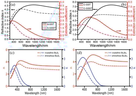
Figure 6.
The relationships between complex refractive index and wavelength of several PCMs. (a) Amorphous Ge2Sb2Te5 (a-GST) and amorphous Ge2Sb2Se4Te1 (a-GSST) [62], (b) crystalline Ge2Sb2Te5 (c-GST) and crystalline Ge2Sb2Se4Te1 (c-GSST) [62], (c) Sb2S3 (SbS) [63], (d) Sb2Se3 (SbSe) [63]. (a,b) reprinted with permission from ref. [62] © The Optical Society.
4.2. State of the Art
As a common PCM, Ge2Sb2Te5 (GST) was widely used in the design of silicon photonic switches. In 2018, Xu et al. demonstrated a low-loss and broadband nonvolatile silicon photonic switch using GST [61]. Based on the 3W DC structure (Figure 7a) and the GST-on-silicon platform, the high absorption of the crystalline state was successfully bypassed (Figure 7b,c). With a compact coupling length of 35 μm, the measured IL and CT of the 2 × 2 switch are about 1 dB and less than −15 dB for cross state and 1~2 dB and less than −10 dB for bar state at the wavelength range of 1510 nm~1540 nm. In 2020, Zhang et al. proposed a wavelength-selective 2 × 2 nonvolatile MRR-based silicon photonic switch assisted by GST-PCM [69]. A simulation showed that the ER of the optical switch is about 20 dB at resonant wavelength, and the ILs at through and drop ports are 0.9 dB and 2 dB, respectively. Particularly, when the switch is switched OFF or ON, the resonant wavelength varies little, making it suitable for the dense WDM systems. In 2022, Chen et al. reported a nonvolatile electrically controlled 2 × 2 silicon photonic switch still based on GST [70]. The 3W DC structure exhibits a compact coupling length of 64 μm. A small IL of about 2 dB and minimal CT of less than −8 dB across the entire C-band are achieved. Driven by an on-chip PIN heater, the device can be switched reliably and reversibly for more than 2800 cycles without significant performance degradation. The proposed nonvolatile silicon photonic switch plays a key role in future programmable silicon photonic systems.
Figure 7.
(a) Schematic of the nonvolatile 2 × 2 silicon photonic switch based on the 3W directional coupler (DC) structure Inset: The cross section of the device. Normalized electric field intensity distribution of the device for (b) a-GST and (c) c-GST at the wavelength of 1550 nm. Reprinted with permission from ref. [61]. Copyright 2019 American Chemical Society.
Due to the large imaginary part of the complex refractive index in both crystalline phase and amorphous phase of GST at the telecommunication band, the devices based on GST usually have high absorption loss, thus limiting its applicability. To address this issue, a new low-loss PCM should be used to replace GST in the design of nonvolatile silicon photonic switches. As shown in Figure 6, the new PCMs, Ge2Sb2Se4Te1 (GSST), Sb2S3 (SbS), and Sb2Se3 (SbSe) all exhibit low attenuation in both states compared with GST. In 2018, Zhang et al. proposed a broadband nonvolatile silicon photonic switch in the C-band with record low IL and CT by using a new PCM GSST and a nonperturbative design [62]. For 2 × 2 switch, the ILs for the cross state and through state are 0.013 dB and 0.32 dB at 1550 nm, and the CTs for the two states are −37 dB and −32 dB, respectively. Furthermore, the device exhibits broadband switching capability across the C-band. The design represented the best performance for nonvolatile optical switches at that time. Jiang demonstrated a three-dimensional (3D) reconfigurable mode (De)multiplexer/switch based on the 3W DC with GSST-PCM [71]. For the TE mode, the IL and ER are 0.38 dB/1.14 dB and 18.25 dB /14.0 dB for the OFF/ON state with a coupling length of 12 μm, respectively. A more compact device can be achieved for the TM mode with a coupling length of 8.28 μm, IL of 0.12 dB/1.98 dB, and CT of −16.37 dB/−13.23 dB for the OFF/ON state, respectively. The proposed device has a potential application in the 3D MDM networks for flexible mode switching and routing. De Leonardis et al. proposed a broadband nonvolatile electro-optic switch based on GSST on SOI [72]. A 2 × 2 nonvolatile electro-optic switch operating in the C-band was realized based on the 3W DC structure with a doped indium-tin oxide (ITO) microstrip heater deposited on the PCM strip. For the coupling length of 15.4 μm, the simulation results show that the IL, CT, and 0.3-dB-IL bandwidth are 0.018 dB, less than −31.3 dB, and 58 nm. While for the coupling length of 17.4 μm, they are 0.046 dB, less than −38.1 dB, and 70 nm, respectively. In 2021, Carlos Ríos et al. realized an electrically driven 2 × 2 MZI nonvolatile silicon photonic switch based on the new PCM, SbSe [73]. While Yang et al. proposed a 2 × 2 nonvolatile MZI silicon photonic switch based on low-loss SbS, which works in the C-band [74]. When working in a single-drive mode (Figure 8a), the Si-SbS hybrid waveguide length is 9 μm to provide a π phase shift. The IL of all switch paths is below 3 dB, and the CT is less than −10 dB in a 10 nm wavelength range for all paths. Then, a push-pull dual-drive structure (Figure 8b) was used to improve the switch performance. Two SbS patches are 3.88 μm in length to offer a π/2 phase shift and an extra amorphous SbS (a-SbS) patch integrated on the lower arm is 1.62 μm long to introduce a fixed phase shift of π/2. In this case, the IL is reduced to 0.6 dB and the CT is below −20 dB for both switching states. The performance metrics of several typical 2 × 2 nonvolatile silicon photonic switches proposed in recent years are summarized in Table 3.
Figure 8.
Schematics of (a) the single-drive hybrid Si-SbS integrated 2 × 2 unbalanced MZI optical switch and (b) a push-pull drive 2 × 2 SbS MZI switch. The inset in (a) shows the cross section of the Si-SbS hybrid waveguide. Reprinted with permission from ref. [74] © The Optical Society.
Table 3.
Comparison of several typical 2 × 2 nonvolatile silicon photonic switches *.
5. Conclusions
The 2 × 2 silicon photonic switches are the key elements in constructing large-scale optical switching matrices and optical routers. The continuous progress of silicon photonic switches, modulators, detectors, and other critical and basic elements promotes the development of silicon photonics. This review article mainly introduces and summarizes the principle and state of the art of several types of 2 × 2 silicon photonic switches, including silicon-based electro-optic switches, silicon-based thermo-optic switches, and nonvolatile silicon photonic switches assisted by PCMs. The research on 2 × 2 silicon photonic switches progressed increasingly. Taking the representative MZI silicon-based electro-optic switch as an example, with the intervention of Intel, IBM, Kotura, etc. and the help of mature CMOS process platform and rich technology accumulation, the performance metrics of 2 × 2 silicon photonic switches such as bandwidth, speed, and power consumption, etc., were significantly improved. It can be predicted that the continuous evolution and development of semiconductor process technology will bring continuous innovation and breakthrough for silicon photonic switches.
Author Contributions
Conceptualization, W.Y.; methodology, W.Y.; software, W.Y.; validation, W.Y. and Y.C.; formal analysis, W.Y. and Y.C.; investigation, W.Y.; resources, W.Y.; data curation, W.Y.; writing—original draft preparation, W.Y.; writing—review and editing, Y.C. and M.Y.; visualization, W.Y.; supervision, W.Y.; project administration, W.Y. and M.Y.; funding acquisition, W.Y. and M.Y. All authors have read and agreed to the published version of the manuscript.
Funding
This research was funded by National Natural Science Foundation of China (NSFC) (62204250); Strategic Pioneer Research Projects of Defense Science and Technology (XDB43020500); Shanghai Sailing Program (20YF1456900).
Institutional Review Board Statement
Not applicable.
Informed Consent Statement
Not applicable.
Data Availability Statement
Data sharing not applicable.
Conflicts of Interest
The authors declare no conflict of interest.
References
- Zhou, Z. Silicon Photonics, 1st ed.; Peking University: Beijing, China, 2012. [Google Scholar]
- Sun, C.; Wade, M.T.; Lee, Y.; Orcutt, J.S.; Alloatti, L.; Georgas, M.S.; Waterman, A.S.; Shainline, J.M.; Avizienis, R.R.; Lin, S. Single-chip microprocessor that communicates directly using light. Nature 2015, 528, 534–538. [Google Scholar] [CrossRef] [PubMed]
- Wang, J.; Paesani, S.; Ding, Y.; Santagati, R.; Skrzypczyk, P.; Salavrakos, A.; Tura, J.; Augusiak, R.; Mancinska, L.; Bacco, D.; et al. Multidimensional quantum entanglement with large-scale integrated optics. Science 2018, 360, 285–291. [Google Scholar] [CrossRef] [PubMed]
- Shen, Y.; Harris, N.C.; Skirlo, S.; Prabhu, M.; Baehr-Jones, T.; Hochberg, M.; Sun, X.; Zhao, S.; Larochelle, H.; Englund, D. Deep learning with coherent nanophotonic circuits. Nat. Photonics 2017, 11, 441–446. [Google Scholar] [CrossRef]
- Zhuang, L.; Roeloffzen, C.G.; Hoekman, M.; Boller, K.-J.; Lowery, A.J. Programmable photonic signal processor chip for radiofrequency applications. Optica 2015, 2, 854–859. [Google Scholar] [CrossRef]
- Liu, W.; Li, M.; Guzzon, R.S.; Norberg, E.J.; Parker, J.S.; Lu, M.; Coldren, L.A.; Yao, J. A fully reconfigurable photonic integrated signal processor. Nat. Photonics 2016, 10, 190–195. [Google Scholar] [CrossRef]
- Graydon, O. Birth of the programmable optical chip. Nat. Photonics 2016, 10, 1. [Google Scholar]
- Perez, D.; Gasulla, I.; Crudgington, L.; Thomson, D.J.; Khokhar, A.Z.; Li, K.; Cao, W.; Mashanovich, G.Z.; Capmany, J. Multipurpose silicon photonics signal processor core. Nat. Commun. 2017, 8, 636. [Google Scholar] [CrossRef]
- Rogers, C.; Piggott, A.Y.; Thomson, D.J.; Wiser, R.F.; Opris, I.E.; Fortune, S.A.; Compston, A.J.; Gondarenko, A.; Meng, F.; Chen, X.; et al. A universal 3D imaging sensor on a silicon photonics platform. Nature 2021, 590, 256–261. [Google Scholar] [CrossRef]
- Harris, N.C.; Steinbrecher, G.R.; Prabhu, M.; Lahini, Y.; Mower, J.; Bunandar, D.; Chen, C.; Wong, F.N.C.; Baehr-Jones, T.; Hochberg, M.; et al. Quantum transport simulations in a programmable nanophotonic processor. Nat. Photonics 2017, 11, 447–452. [Google Scholar] [CrossRef]
- Arrazola, J.M.; Bergholm, V.; Brádler, K.; Bromley, T.R.; Collins, M.J.; Dhand, I.; Fumagalli, A.; Gerrits, T.; Goussev, A.; Helt, L.G.; et al. Quantum circuits with many photons on a programmable nanophotonic chip. Nature 2021, 591, 54–60. [Google Scholar] [CrossRef]
- Wu, M.C.; Solgaard, O.; Ford, J.E. Optical MEMS for lightwave communication. J. Lightwave Technol. 2006, 24, 4433–4454. [Google Scholar] [CrossRef]
- Tanaka, S.; Jeong, S.; Yamazaki, S.; Uetake, A.; Tomabechi, S.; Ekawa, M.; Morito, K. Monolithically integrated 8:1 SOA gate switch with large extinction ratio and wide input power dynamic range. IEEE J. Sel. Top. Quantum Electron. 2009, 45, 1155–1162. [Google Scholar] [CrossRef]
- Frisken, S.; Baxter, G.; Abakoumov, D.; Hao, Z.; Clarke, I.; Poole, S. Flexible and grid-less wavelength selective switch using LCOS technology. In Proceedings of the Optical Fiber Communication Conference and Exposition, Los Angeles, CA, USA, 6–10 March 2011; pp. 1–3. [Google Scholar] [CrossRef]
- Asakawa, K.; Sugimoto, Y.; Ikeda, N.; Watanabe, Y.; Ozaki, N.; Takata, Y.; Kitagawa, Y.; Ohkouchi, S.; Nakamura, S.; Watanabe, A.; et al. Photonic crystal all-optical switches. In Optical Switches; Li, B., Chua, S.J., Eds.; Woodhead Publishing: Cambridge, UK, 2010; pp. 241–275. [Google Scholar] [CrossRef]
- Lee, B.G.; Dupuis, N.; Pepeljugoski, P.; Schares, L.; Budd, R.; Bickford, J.R.; Schow, C.L. Silicon photonic switch fabrics in computer communications systems. J. Lightwave Technol. 2015, 33, 768–777. [Google Scholar] [CrossRef]
- Li, Y.; Zhang, Y.; Zhang, L.; Poon, A.W. Silicon and hybrid silicon photonic devices for intra-datacenter applications: State of the art and perspectives. Photonics Res. 2015, 3, B10–B27. [Google Scholar] [CrossRef]
- Cheng, Q.; Rumley, S.; Bahadori, M.; Bergman, K. Photonic switching in high performance datacenters. Opt. Express 2018, 26, 16022–16043. [Google Scholar] [CrossRef]
- Yao, Z.; Wu, K.; Tan, B.X.; Wang, J.; Li, Y.; Zhang, Y.; Poon, A.W. Integrated silicon photonic microresonators: Emerging technologies. IEEE J. Sel. Top. Quantum Electron. 2018, 24, 5900324. [Google Scholar] [CrossRef]
- Tu, X.; Song, C.; Huang, T.; Chen, Z.; Fu, H. State of the art and perspectives on silicon photonic switches. Micromachines 2019, 10, 51. [Google Scholar] [CrossRef]
- Soref, R.A.; Bennett, B.R. Electrooptical effects in silicon. IEEE J. Quant. Electron. 1987, 23, 123–129. [Google Scholar] [CrossRef]
- Reed, G.T.; Mashanovich, G.; Gardes, F.Y.; Thomson, D.J. Silicon optical modulators. Nat. Photonics 2010, 4, 518–526. [Google Scholar] [CrossRef]
- Lorenzo, J.P.; Soref, R.A. 1.3 μm electro-optic silicon switch. Appl. Phys. Lett. 1987, 51, 6–8. [Google Scholar] [CrossRef]
- Soref, R.A.; Lorenzo, J.P. All-silicon active and passive guided-wave components for λ = 1.3 and λ = 1.6 μm. IEEE J. Quantum Electron. 1986, 22, 873–879. [Google Scholar] [CrossRef]
- Lee, B.G.; Green, W.; Campenhout, J.V.; Schow, C.L. Comparison of ring resonator and Mach-Zehnder photonic switches integrated with digital CMOS drivers. In Proceedings of the 23rd Annual Meeting of the IEEE Photonics Society, Denver, CO, USA, 7–11 November 2010; pp. 327–328. [Google Scholar]
- Wang, W.; Zhao, Y.; Zhou, H.; Hu, T.; Yang, J.; Wang, M.; Jiang, X. Mach-Zehnder based 2 × 2 electro-optical switches on silicon-on-insulator with low crosstalk. In Proceedings of the 9th International Conference on Group IV Photonics, San Diego, CA, USA, 29–31 August 2012; pp. 300–302. [Google Scholar] [CrossRef]
- Xing, J.; Li, Z.; Yu, Y.; Yu, J. Low cross-talk 2 × 2 silicon electro-optic switch matrix with a double-gate configuration. Opt. Lett. 2013, 38, 4774–4776. [Google Scholar] [CrossRef] [PubMed]
- Dong, P.; Liao, S.; Liang, H.; Shafiiha, R.; Feng, D.Z.; Li, G.L.; Zheng, X.Z.; Krishnamoorthy, A.V.; Asghari, M. Submilliwatt, ultrafast and broadband electro-optic silicon switches. Opt. Express 2010, 18, 252251–252257. [Google Scholar] [CrossRef] [PubMed]
- Lu, L.; Zhou, L.; Li, X.; Chen, J. Low-power 2 × 2 silicon electro-optic switches based on double-ring assisted Mach–Zehnder interferometers. Opt. Lett. 2014, 39, 1633–1636. [Google Scholar] [CrossRef]
- Dupuis, N.; Lee, B.G.; Rylyakov, A.V.; Kuchta, D.M.; Baks, C.W.; Orcutt, J.S.; Gill, D.M.; Green, W.M.J.; Schow, C.L. Design and fabrication of low-insertion-loss and low-crosstalk broadband 2 × 2 Mach-Zehnder silicon photonic switches. J. Lightwave Technol. 2015, 33, 3597–3606. [Google Scholar] [CrossRef]
- Xing, J.; Li, Z.; Zhou, P.; Gong, Y.; Yu, Y.; Tan, M.; Yu, J. Compact silicon-on-insulator-based 2 × 2 Mach–Zehnder interferometer electro-optic switch with low crosstalk. Chin. Opt. Lett. 2015, 13, 061301. [Google Scholar] [CrossRef]
- Dupuis, N.; Rylyakov, A.V.; Schow, C.L.; Kuchta, D.M.; Baks, C.W.; Orcutt, J.S.; Gill, D.M.; Green, W.M.J.; Lee, B.G. Ultralow crosstalk nanosecond-scale nested 2 × 2 Mach-Zehnder silicon photonic switch. Opt. Lett. 2016, 41, 3002–3005. [Google Scholar] [CrossRef]
- Dehghani, F.; Abdollahi, M.; Mohammadi, S.; Barekatain, B. HDMS: High-performance dual-shaped microring-resonator-based optical switch. Opt. Eng. 2022, 61, 035105. [Google Scholar] [CrossRef]
- Sun, C.; Wei, M.; Tang, B.; Ma, H.; Zhang, P.; Luo, Y.; Jian, J.; Li, L.; Lin, H. High-performance silicon pin diode switches in the 2-μm wave band. Opt. Lett. 2022, 47, 2758–2761. [Google Scholar] [CrossRef]
- Campenhout, J.V.; Green, W.M.J.; Assefa, S.; Vlasov, Y.A. Low-power, 2 × 2 silicon electro-optic switch with 110-nm bandwidth for broadband reconfigurable optical networks. Opt. Express 2009, 17, 24020–24029. [Google Scholar] [CrossRef]
- Calò, G.; D’Orazio, A.; Petruzzelli, V. Broadband Mach-Zehnder switch for photonic networks on chip. J. Lightwave Technol. 2012, 30, 944–952. [Google Scholar] [CrossRef]
- Cocorullo, G.; Della Corte, F.G.; Rendina, I. Temperature dependence of the thermo-optic coefficient in crystalline silicon between room temperature and 550 K at the wavelength of 1523 nm. Appl. Phys. Lett. 1999, 74, 3338–3340. [Google Scholar] [CrossRef]
- Dai, D.; Shan, H.; Song, L.; Wang, S. Reconfigurable silicon photonics: Devices and circuits. In Proceedings of the SPIE Optics + Optoelectronics Conference, Integrated Optics: Physics and Simulations III, Prague, Czech Republic, 17 May 2017. [Google Scholar] [CrossRef]
- Li, X.; Xu, H.; Xiao, X.; Li, Z.; Yu, Y.; Yu, J. Fast and efficient silicon thermo-optic switching based on reverse breakdown of pn junction. Opt. Lett. 2014, 39, 751–753. [Google Scholar] [CrossRef] [PubMed]
- Watts, M.R.; Sun, J.; DeRose, C.; Trotter, D.C.; Young, R.W.; Nielson, G.N. Adiabatic thermo-optic Mach-Zehnder switch. Opt. Lett. 2013, 38, 733–735. [Google Scholar] [CrossRef]
- Yu, L.; He, S.; Zheng, J.; Dai, D. Graphene-based transparent nano-heater for thermally-tuning silicon nanophotonic integrated devices. In Proceedings of the Progress in Electromagnetics Research Symposium, Guangzhou, China, 25–28 August 2014; pp. 1735–1738. [Google Scholar]
- Yan, S.; Zhu, X.; Frandsen, L.H.; Xiao, S.; Asger Mortensen, N.; Dong, J.; Ding, Y. Slow-light-enhanced energy efficiency for graphene microheaters on silicon photonic crystal Waveguides. Nat. Commun. 2017, 8, 14411. [Google Scholar] [CrossRef]
- Fang, Q.; Song, J.; Liow, T.Y.; Cai, H.; Yu, M.; Lo, G.; Kwong, D.L. Ultralow power silicon photonics thermo-optic switch with suspended phase arms. IEEE Photonics Technol. Lett. 2011, 23, 525–527. [Google Scholar] [CrossRef]
- He, G.; Ji, L.; Gao, Y.; Liu, R.; Sun, X.; Yi, Y.; Wang, X.; Chen, C.; Wang, F.; Zhang, D. Low power 1 × 4 polymer/SiO2 hybrid waveguide thermo-optic switch. Opt. Commun. 2017, 402, 422–429. [Google Scholar] [CrossRef]
- Chen, K.; Duan, F.; Yu, Y. Performance-enhanced silicon thermo-optic Mach-Zehnder switch using laterally supported suspended phase arms and efficient electrodes. Opt. Lett. 2019, 44, 951–954. [Google Scholar] [CrossRef]
- Duan, F.; Chen, K.; Chen, D.; Yu, Y. Low-power and high-speed 2 × 2 thermo-optic MMI-MZI switch with suspended phase arms and heater-on-slab structure. Opt. Lett. 2020, 46, 234–237. [Google Scholar] [CrossRef]
- Jacques, M.; Samani, A.; El-Fiky, E.; Patel, D.; Xing, Z.; Plant, D.V. Optimization of thermo-optic phase-shifter design and mitigation of thermal crosstalk on the SOI platform. Opt. Express 2019, 27, 10456–10471. [Google Scholar] [CrossRef]
- Kita, T.; Mendez-Astudillo, M. Ultrafast silicon MZI optical switch with periodic electrodes and integrated heat sink. J. Lightwave Technol. 2021, 39, 5054–5060. [Google Scholar] [CrossRef]
- Selvaraja, S.K.; Bogaerts, W.; Dumon, P.; Thourhout, D.V.; Baets, R. Subnanometer linewidth uniformity in silicon nanophotonic waveguide devices using CMOS fabrication technology. IEEE J. Sel. Top. Quantum Electron. 2010, 16, 316–324. [Google Scholar] [CrossRef]
- Espinola, R.L.; Tsai, M.C.; Yardley, J.T.; Osgood, R.M. Fast and low-power thermooptic switch on thin silicon-on-insulator. IEEE Photon. Technol. Lett. 2003, 15, 1366–1368. [Google Scholar] [CrossRef]
- Song, L.; Li, H.; Dai, D. Mach-Zehnder silicon-photonic switch with low random phase errors. Opt. Lett. 2021, 46, 78–81. [Google Scholar] [CrossRef]
- Winzer, P.J.; Neilson, D.T.; Chraplyvy, A.R. Fiber-optic transmission and networking: The previous 20 and the next 20 years. Opt. Express 2018, 26, 24190–24239. [Google Scholar] [CrossRef]
- Hao, J.; Zhou, T.; Lei, Z.; Ding, J.; Xin, F.; Lin, Y. Optical switch compatible with wavelength division multiplexing and mode division multiplexing for photonic networks-on-chip. Opt. Express 2017, 25, 20698–20707. [Google Scholar]
- Zhang, Y.; Zhang, R.; Zhu, Q.; Yuan, Y.; Su, Y. Architecture and devices for silicon photonic switching in wavelength, polarization and mode. J. Lightwave Technol. 2019, 38, 215–225. [Google Scholar] [CrossRef]
- Hang, D.N.T.; Duy, H.T.; Thanh, T.T.T.; Khoi, N.D.H.; Truong, C.D. Compact, highly efficient, and controllable simultaneous 2 × 2 three-mode silicon photonic switch in the continuum band. IEEE Access 2021, 9, 102387–102396. [Google Scholar] [CrossRef]
- Zhang, G.; Xu, D.; Grinberg, Y.; Liboiron-Ladouceur, O. Efficient mode exchanger-based silicon photonic switch enabled by inverse design. Opt. Express 2022, 30, 20543–20553. [Google Scholar] [CrossRef]
- De Galarreta, C.R.; Sinev, I.; Alexeev, A.M.; Trofimov, P.; Ladutenko, K.; Carrillo, S.G.-C.; Gemo, E.; Baldycheva, A.; Bertolotti, J.; Wright, C.D. Reconfigurable multilevel control of hybrid all-dielectric phase-change metasurfaces. Optica 2020, 7, 476–484. [Google Scholar] [CrossRef]
- Youngblood, N.; Rios, C.; Gemo, E.; Feldmann, J.; Cheng, Z.; Baldycheva, A.; Pernice, W.H.P.; Wright, C.D.; Bhaskaran, H. Tunable volatility of Ge2Sb2Te5 in integrated photonics. Adv. Funct. Mater. 2019, 29, 1807571. [Google Scholar] [CrossRef]
- Wang, Y.; Landreman, P.; Schoen, D.; Okabe, K.; Brongersma, M.L. Electrical tuning of phase-change antennas and metasurfaces. Nat. Nanotechnol. 2021, 16, 667–672. [Google Scholar] [CrossRef] [PubMed]
- Qu, Y.; Qiang, L.; Du, K.; Lu, C.; Min, Q. Dynamic thermal emission control based on ultrathin plasmonic metamaterials including phase-changing material GST. Laser Photonics Rev. 2017, 11, 1700091. [Google Scholar] [CrossRef]
- Xu, P.; Zheng, J.; Doylend, J.K.; Majumdar, A. Low-loss and broadband nonvolatile phase-change directional coupler switches. ACS Photonics 2019, 6, 553–557. [Google Scholar] [CrossRef]
- Zhang, Q.; Zhang, Y.; Li, J.; Soref, R.; Gu, T.; Hu, J. Broadband nonvolatile photonic switching based on optical phase change materials: Beyond the classical figure-of-merit. Opt. Lett. 2018, 43, 94–97. [Google Scholar] [CrossRef] [PubMed]
- Delaney, M.; Zeimpekis, I.; Lawson, D.; Hewak, D.W.; Muskens, O.L. A new family of ultralow loss reversible phase-change materials for photonic integrated circuits: Sb2S3 and Sb2Se3. Adv. Funct. Mater. 2020, 30, 2002447. [Google Scholar] [CrossRef]
- Shportko, K.; Kremers, S.; Woda, M.; Lencer, D.; Robertson, J.; Wuttig, M. Resonant bonding in crystalline phase-change materials. Nat. Mater. 2008, 7, 653–658. [Google Scholar] [CrossRef] [PubMed]
- Orava, J.; Greer, A.L.; Gholipour, B.; Hewak, D.W.; Smith, C.E. Characterization of supercooled liquid Ge2Sb2Te5 and its crystallization by ultrafast-heating calorimetry. Nat. Mater. 2012, 11, 279–283. [Google Scholar] [CrossRef] [PubMed]
- Loke, D.; Lee, T.H.; Wang, W.J.; Shi, L.P.; Zhao, R.; Yeo, Y.C.; Chong, T.C.; Elliott, S.R. Breaking the speed limits of phase-change memory. Science 2012, 336, 1566–1569. [Google Scholar] [CrossRef] [PubMed]
- Raoux, S.; Xiong, F.; Wuttig, M.; Pop, E. Phase change materials and phase change memory. MRS Bull. 2014, 39, 703–710. [Google Scholar] [CrossRef]
- Raoux, S.; Burr, G.W.; Breitwisch, M.J.; Rettner, C.T.; Lam, C.H. Phase-change random access memory: A scalable technology. IBM J. Res. Dev. 2008, 52, 465–479. [Google Scholar] [CrossRef]
- Zhang, C.; Zhang, M.; Xie, Y.; Shi, Y.; Kumar, R.; Panepucci, R.R.; Dai, D. Wavelength-selective 2 × 2 optical switch based on a Ge2Sb2Te5-assisted microring. Photonics Res. 2020, 8, 1171–1176. [Google Scholar] [CrossRef]
- Chen, R.; Fang, Z.; Fröch, J.E.; Xu, P.; Zheng, J.; Majumdar, A. Broadband nonvolatile eectrically controlled programmable units in silicon photonics. ACS Photon. 2022, 9, 2142–2150. [Google Scholar] [CrossRef]
- Jiang, W. Reconfigurable mode (de) multiplexer via 3D triple-waveguide directional coupler with optical phase change material. J. Lightwave Technol. 2018, 37, 1000–1007. [Google Scholar] [CrossRef]
- De Leonardis, F.; Soref, R.; Passaro, V.M.N.; Zhang, Y.; Hu, J. Broadband electro-optical crossbar switches using low-loss Ge2Sb2Se4Te1 Phase Change Material. J. Lightwave Technol. 2019, 37, 3183–3191. [Google Scholar] [CrossRef]
- Ríos, C.; Du, Q.; Zhang, Y.; Popescu, C.-C.; Shalaginov, M.Y.; Miller, P.; Roberts, C.; Kang, M.; Richardson, K.A.; Gu, T.; et al. Ultra-compact nonvolatile phase shifter based on electrically reprogrammable transparent phase change materials. PhotoniX 2022, 3, 26. [Google Scholar] [CrossRef]
- Yang, X.; Nisar, M.S.; Yuan, W.; Zheng, F.; Lu, L.; Chen, J.; Zhou, L. Phase change material enabled 2 × 2 silicon nonvolatile optical switch. Opt. Lett. 2021, 46, 4224–4227. [Google Scholar] [CrossRef]


Disclaimer/Publisher’s Note: The statements, opinions and data contained in all publications are solely those of the individual author(s) and contributor(s) and not of MDPI and/or the editor(s). MDPI and/or the editor(s) disclaim responsibility for any injury to people or property resulting from any ideas, methods, instructions or products referred to in the content. |
© 2023 by the authors. Licensee MDPI, Basel, Switzerland. This article is an open access article distributed under the terms and conditions of the Creative Commons Attribution (CC BY) license (https://creativecommons.org/licenses/by/4.0/).