Review

Sb-Based Low-Noise Avalanche Photodiodes

1
Department of Electrical and Computer Engineering, University of Virginia, Charlottesville, VA 22904, USA
2
Department of Electronic and Electrical Engineering, University of Sheffield, Sheffield S1 3JD, UK
3
Department of Electrical and Computer Engineering, University of Texas, Austin, TX 78758, USA
*
Author to whom correspondence should be addressed.
Photonics 2023, 10(7), 715; https://doi.org/10.3390/photonics10070715
Submission received: 15 May 2023 / Revised: 8 June 2023 / Accepted: 17 June 2023 / Published: 22 June 2023
(This article belongs to the Special Issue Advances in Avalanche Photodiodes)

Abstract

:
Accurate detection of weak optical signals is a key function for a wide range of applications. A key performance parameter is the receiver signal-to-noise ratio, which depends on the noise of the photodetector and the following electrical circuitry. The circuit noise is typically larger than the noise of photodetectors that do not have internal gain. As a result, a detector that provides signal gain can achieve higher sensitivity. This is accomplished by increasing the photodetector gain until the noise associated with the gain mechanism is comparable to that of the output electrical circuit. For avalanche photodiodes (APDs), the noise that arises from the gain mechanism, impact ionization, increases with gain and depends on the material from which the APD is fabricated. Si APDs have established the state-of-the-art for low-noise gain for the past five decades. Recently, APDs fabricated from two Sb-based III-V compound quaternary materials, AlxIn1-xAsySb1-y and AlxGa1-xAsySb1-y, have achieved noise characteristics comparable to those of Si APDs with the added benefit that they can operate in the short-wave infrared (SWIR) and extended SWIR spectral regions. This paper describes the materials and device characteristics of these APDs and their performance in different spectral regions.

1. Introduction

Essentially all devices that demonstrate gain also exhibit noise associated with the underlying signal amplification mechanism. The benefit of gain is achieved when an improvement in the signal-to-noise performance (S/N) is realized. For avalanche photodiodes (APDs), the gain mechanism is impact ionization, and noise arises from its stochastic characteristic. If thermal and quantum noise are negligible compared to shot noise, the advantage of a receiver that uses an APD with gain, M, as the detector compared to a PIN detector is illustrated by the expression
( S N ) A P D ( S N ) P I N = 2 q i p h + i d a r k f + i 2 c i r c u i t 2 q i p h + i d a r k F f + i 2 c i r c u i t M 2
where iph and idark are the photocurrent and dark current, respectively. The circuit current noise is icircuit, and Δf is the receiver bandwidth. The excess noise factor, F, is a measure of the nondeterminism of the gain. It is clear that gain reduces the effect of electronic noise, but this is mitigated by the excess noise factor, which becomes more detrimental with increasing gain. Since the signal strength increases with gain, the optimum signal-to-noise performance occurs at a gain where total detector noise equals the input noise of the electrical circuitry. The performance advantage for systems that rely on the detection of information encoded on an optical signal has benefited a wide range of applications, including telecommunications [1], data centers [2], spectroscopy [3,4], imaging [5], LIDAR [6], medical diagnostics [7,8], and quantum applications [9,10].
The excess noise factor varies with material and device structure. In the local field model, which provides good fits to the noise of APDs in which the non-local nature of impact ionizations is not significant, the excess noise factor is expressed as F = k · M + (1 − k) · (2 − 1/M) [11], where k is the ratio of the hole ionization coefficient, β, to that of the electron, α. While the excess noise factor increases with gain, it does so more slowly for materials that exhibit low k-values. It is for this reason that Si, which generates k-values in the range 0.01 to 0.02, has been the APD of choice in the spectral range dictated by its bandgap energy, namely visible to near-infrared (~400 nm to 950 nm).
Recently, two bulk quaternary materials, AlxGa1-xAsySb1-y lattice-matched to InP and AlxIn1-xAsySb1-y to GaSb, have exhibited excess noise comparable to Si. Compared to Si, these materials have the added advantage that their bandgap energies can be adjusted to operate in the short-wave infrared (SWIR, 950 nm to 1700 nm) and extended SWIR (eSWIR, 1700 nm to 2200 nm) spectral regions. Higher Al concentrations produce wide-bandgap material that can be used as homojunction detectors in the near-infrared. Operation in the SWIR and eSWIR requires narrow-bandgap materials that use separate absorption and multiplication structures to circumvent the tunneling component of the dark current. This paper presents the electrical and optical performance of these Sb-based APDs.

2. Materials and Methods

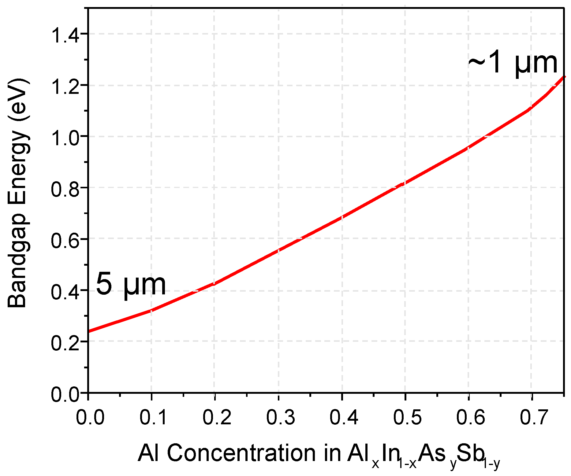
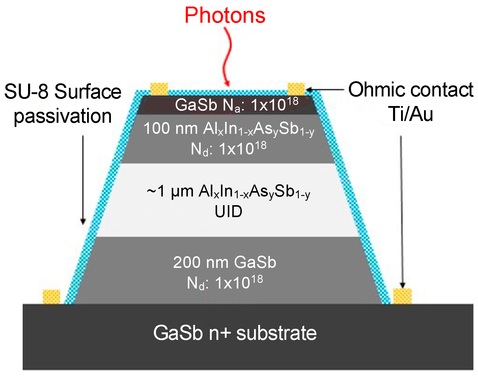
2.1. AlxIn1-xAsySb1-y on GaSb Substrate

The epitaxial layers were grown on n-type Te-doped GaSb (001) substrates by solid-source molecular beam epitaxy (MBE) at 460 °C, as determined by blackbody thermometry (k-Space BandiT). Typically, alloy III-V alloy semiconductors are grown as random alloys where the different types of atoms on the column III sites or column V sites are distributed randomly. However, for the AlxIn1-xAsySb1-y material system there is a miscibility issue that leads to islanding and inhomogeneous growth. To circumvent this difficulty, in the AlxIn1-xAsySb1-y material system, these layers were grown as a digital alloy of the binary alloys AlAs, AlSb, InAs, and InSb, using the following layer sequence: AlSb, AlAs, AlSb, InSb, InAs, Sb [12,13]. As shown in Figure 1, the equivalent bandgap energy can be tuned from ~1 µm to 5 µm by changing the Al concentration. In the following, AlxGa1-xAsySb1-y will be referred to by the Al concentration as AlxInAsSb. Solid-source valved-crackers provided As2 and Sb fluxes, and solid-source effusion cells provided Al, Ga, In, Be (acceptor), and GaTe (donor) fluxes.
Circular mesas were defined by standard photolithography processes and etched via an N2/Cl2 inductively coupled plasma. Following the mesa etch, the exposed sidewalls were smoothed with a dilute bromine–methanol solution. Both P and N titanium/gold contacts were deposited by electron-beam evaporation, and the mesa sidewalls were passivated with SU-8 to reduce surface leakage.

2.2. AlxGa1-xAs0.56Sb0.44 on InP Substrate

Epitaxial layers of AlxGa1-xAs0.56Sb0.44 can be grown lattice-matched to InP using MBE. However, due to similar concerns as for AlxIn1-xAsySb1-y on GaSb regarding phase separation and the miscibility gap when growing thick layers of AlxGa1-xAs0.56Sb0.44 on InP, initial attempts at growing AlAs0.56Sb0.44 [14,15] used a very-short-period (13 Å) superlattice of AlAs (1.7 Å) and AlSb (11.4 Å). The As2 and Sb2 fluxes in this digital alloy growth (DA) were controlled using valved cracker cells, enabling AlAs0.56Sb0.44 of 1950 nm thickness to be grown on InP. AlAs0.56Sb0.44 tends to oxidize readily when exposed to air, leading to high surface leakage currents in mesa structures [16]. The target period of the DA used here was 1.3 nm. More recently, it was found that using a reduced growth temperature of the Al0.85Ga0.15As0.56Sb0.44 alloy of 450C avoided the phase separation issue by suppressing the surface adatom mobility. Successful random alloy growth of Al0.85Ga0.15As0.56Sb0.44 was undertaken using a growth rate of 0.5 μm/h and a V/III flux ratio of ~5 [17].

3. Results

3.1. AlxIn1-xAsySb1-y p-i-n Structure APDs

Initially, to investigate the characteristics of AlxIn1-xAsySb1-y as an APD, p-i-n structures with x = 0.7 to 0.15 were fabricated [18]. A schematic cross-section is shown in Figure 2. The dark current density versus bias voltage of x = 0.7, 0.3, and 0.15 devices is shown in Figure 3.
These compositions correspond to cutoff wavelengths of 1 µm, 2 µm, and 3 µm, respectively. Measurements of the dark current versus device diameter indicated that for the wider-bandgap materials (x ≥ 0.6), surface leakage was the dominant dark current component. In contrast, in lower-bandgap compositions, the dark current originated in the bulk, with a strong tunneling component. The wider-bandgap APDs exhibited gains as high as 100.
Figure 4 shows the excess noise factor versus gain for an Al0.7InAsSb APD. Pure electron injection was achieved by illuminating with 445 nm light. The dashed lines are plots of the excess noise for k-values of 0, 0.05, and 0.1 using the local-field model [11]. The k-values for a commercial Si APD are shown for reference and fall between 0.01 and 0.05. A consideration for accurately determining the excess noise is that the depletion layer width increases slightly toward the surface as the bias increases. This can increase the responsivity, which can result in errors in determining the gain. To account for the bias-dependent responsivity, the correction technique developed by Woods et al. [19] has been applied to the data in Figure 4.
AlInAsSb PIN APDs grown as a random alloy by MBE on InP substrates have also been reported [20]. Growth on InP substrates enables illumination through the substrate, eliminating the need for substrate removal when bonding arrays to readout circuits. It is also beneficial that high-quality InP substrates are available up to 6 inches in diameter, an advantage for manufacturing. Semi-insulating InP substrates are an advantage for high-bandwidth applications. S. H. Kodati et al. reported dark current densities as low as 55 µA/cm2 at a gain of 10 at 300 K [16]. Like the digital alloy AlInAsSb APDs, the noise of the random alloy devices was very low, characterized by a k-value of ~0.02, which calls into question the distinction between digital and random alloys.
Recently, to gain insight into the origin of low noise in Sb-based APDs, S. K. Ahmed et al. [21] studied the AlInAsSb alloy valence band carrier transport using non-equilibrium Green’s functions and Boltzmann transport equation formalisms. Their analysis showed that when the minigaps and the light-hole split-off energy gap are sufficiently large, they create barriers that are improbable to be overcome by quantum tunneling or phonon scattering processes. This impedes hole impact ionization in this material and improves the excess noise performance.

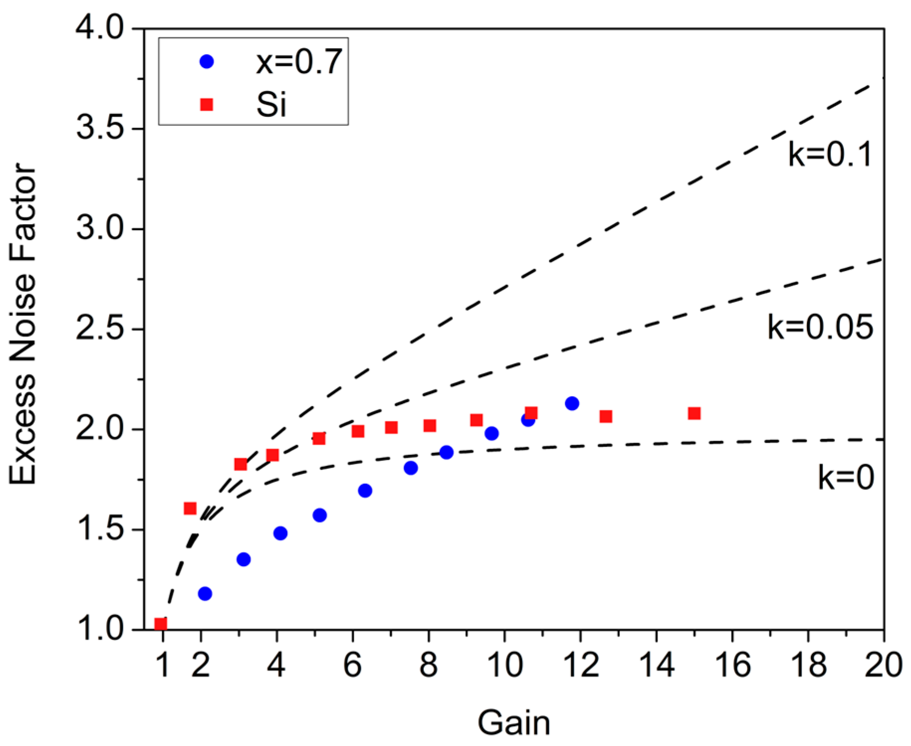
3.2. AlxIn1-xAsySb1-y Separate Absorption, Charge, and Multiplication APDs
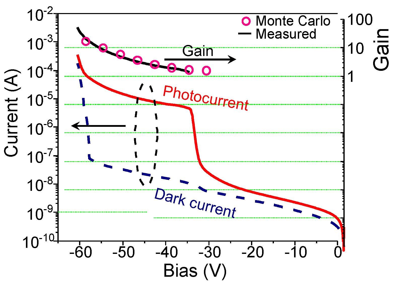
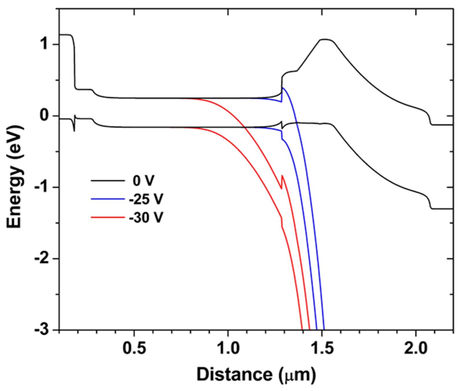
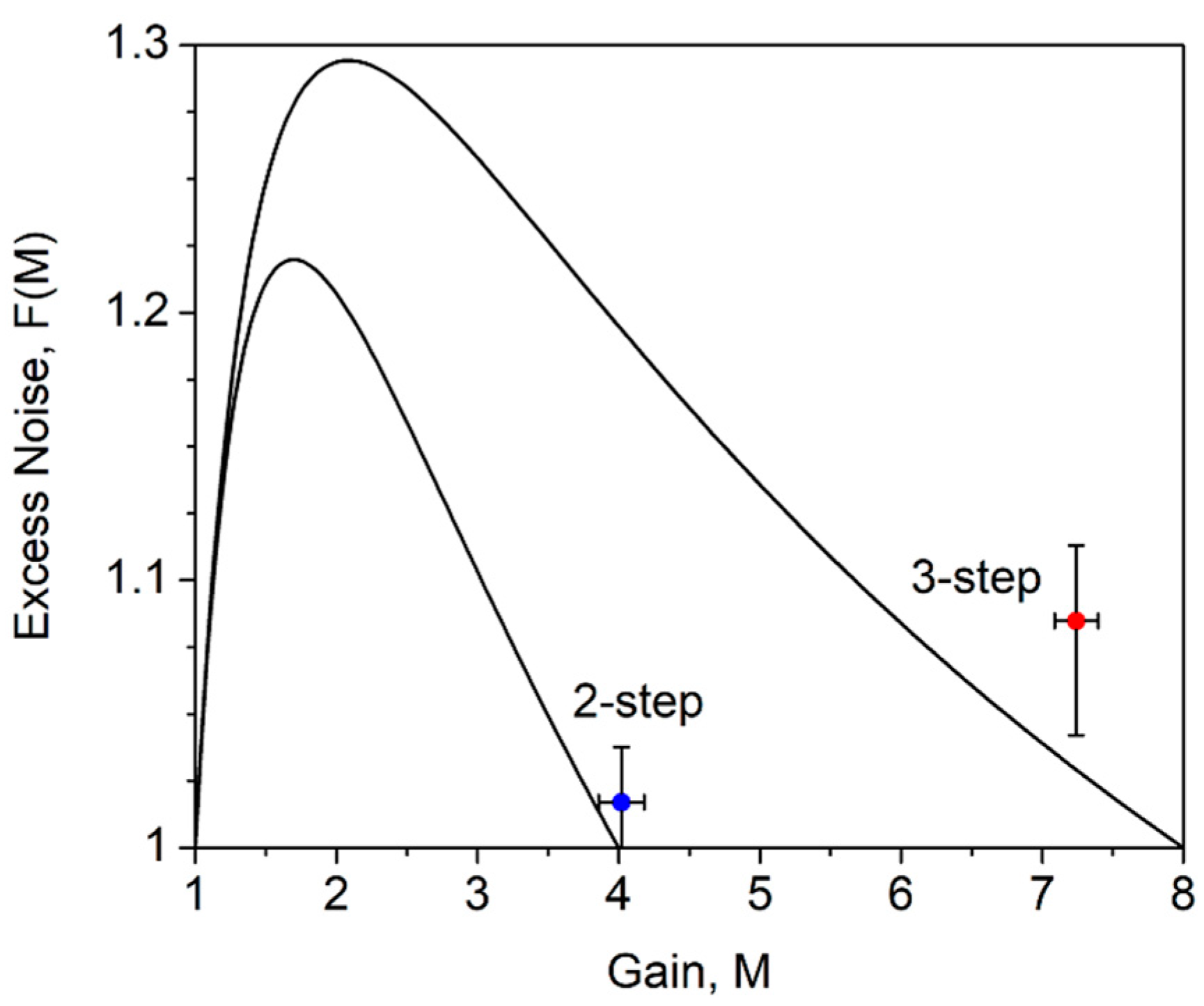
It is clear from the dark current plots in Figure 3 that the dark current of compositions that can operate in the SWIR and eSWIR is too high and will severely limit the SNR. This is due to the prevalence of tunneling in the narrow-bandgap materials and the high electric fields requisite for impact ionization. A common approach to avoid this limitation is to use separate absorption, charge, and multiplication (SACM) structures. In these APDs, the p-n junction and, thus, the high-field multiplication region are located in an undoped wide-bandgap semiconductor where tunneling is insignificant and absorption occurs in an adjacent narrow-bandgap layer. These two regions are separated by a wide-bandgap doped charge layer that is used to tailor the electric field profile so that the field in the multiplication layer is sufficiently high to achieve significant gain and simultaneously maintain a low field in the absorber to suppress tunneling. Compositionally graded layers are positioned on each side of the absorption layer to reduce charge accumulation at the heterojunction interfaces. Figure 5 is a cross-sectional schematic of an Al0.7InAsSb/AlxInAsSb SACM APD.
An Al0.4InAsSb absorption layer was used to achieve operation at 1550 nm. The dark current, photocurrent, and gain versus bias voltage of a 50 µm diameter device are shown in Figure 6. The dark current at 95% breakdown was ~120 nA, which is approximately 100 times lower than that of Ge on Si APDs [22,23] and comparable to AlInAs/InGaAs APDs [24]. Gain values as high as 90 have been observed. The external quantum efficiency at 1550 nm was 35%. We note that there was no anti-reflection coating, and the absorption layer was only 1 µm thick. Higher quantum efficiency, particularly at longer wavelengths, can be achieved with thicker absorption layers and by adding an anti-reflection coating to the top surface. The excess noise factor was similar to that measured for the 70% p-i-n APD shown in Figure 4.
To extend the operation of the AlInAsSb SACM APD to a longer wavelength, the Al0.4InAsSb absorption layer was replaced with narrower-bandgap Al0.3InAsSb (~0.58 eV) [25]. AlInAsSb exhibits the unique characteristic of a minimal valence band discontinuity within a wide range of bandgap energies (from 0.247 eV to 1.68 eV) [26]. Since the change in the AlxInAsSb bandgap is primarily in the conduction band and electrons heavily dominate impact ionization, the design of the charge layer provides a challenge. This layer must deplete so that the conduction band barrier sufficiently lowers to allow photo-generated carriers into the multiplication region without enabling band-to-band tunneling in the absorber. This was accomplished by optimizing the doping and thickness of the charge layer and continuous grading of the bandgap from the absorber to the multiplication region. The dark current density at 200 K was 3 × 10⁻⁴ A/cm2 at M = 10, comparable to HgCdTe at 120 K for the same gain. Under 2 µm illumination, the gain was >100, and the k-value was 0.01.
The cutoff wavelength was extended to 3 µm by further reducing the Al composition to 0.15; in this case, the absorber was doped p-type [27]. This prevents the absorber from fully depleting at punch-through, i.e., the voltage at which the depletion edge reaches the absorber. The net result is a decrease in the dark current. The multiplication region remained Al0.7InAsSb. The charge layer consisted of three distinct layers, all p-type (1 × 1017 cm−3). Starting from the unintentionally doped multiplication layer, a thin layer of the wide-bandgap Al0.7InAsSb was grown. Then, the composition was linearly graded down to Al0.4InAsSb. Finally, a thin layer of Al0.4InAsSb was grown to complete the doped charge region. This final portion of the charge region was added to mitigate the high fields in the charge layer as the device is depleted. Since the field in the charge region will ultimately be much higher than in the absorber, this wider-bandgap layer is designed to protect the device from premature tunneling breakdown. This design limited charge trapping at the conduction band interfaces and high electric fields in the absorber. The energy band diagrams for different bias voltages are shown in Figure 7. The dark current density versus bias voltage from 100 K to 300 K is plotted in Figure 8. At 240 K, a maximum gain of 50 was obtained under 2 μm illumination. InAs, which has a comparable optical cutoff, is commonly limited to low-gain operation (M < 50), even when cooled to 77 K [28,29]. At the same illumination wavelength, an EQE of 65% at the punch-through voltage without an anti-reflection coating was observed.
The cutoff wavelength was extended further into the MWIR by decreasing the Al concentration in the absorber to 0.15 [30]. Under 2 μm illumination at 100 K, these APDs exhibited gains over 850. The excess noise factor scales with a low k-factor of ~0.04. The unity-gain external quantum efficiency of the device peaked at 54% (1.02 A/W) at 2.35 μm and maintained an efficiency of 24% (0.58 A/W) at 3 μm before cutting off at ~3.5 μm. At a gain of 850, the device has a gain-normalized dark current density of 0.05 mA/cm2. Compared with the previously reported MWIR Al0.15InAsSb-based SACM [27], at 100 K this device has a gain-normalized DCD over two orders of magnitude lower, 0.05 mA/cm2 compared with 6 mA/cm2. HgCdTe is a widely used materials system for MWIR detection and amplification with devices exhibiting high gain, up to 5300 [31], and near-unity excess noise [32]. However, in addition to environmental concerns, HgCdTe is a difficult materials system to work with specifically regarding low-defect-density crystal growth and p-type doping. A popular III-V alternative to HgCdTe for detection below ~3.5 µm is InAs as it too has a low excess noise factor near unity [33]. Several device implementations exist [34,35]; however, when operating at 77 K, in order to reduce the impact of band-to-band tunneling on the dark current, the gain peaks at ~30. Operating at higher temperatures yields increased gains, up to ~300; however, the dark current of these devices is poor due to band-to-band tunneling. With InAs, there is a tradeoff between high gain and low dark current density. Additionally, InAs structures incorporate thick intrinsic regions, up to 8 μm thick, to achieve gain while keeping the electric field low enough to suppress band-to-band tunneling. These thick intrinsic regions not only make it difficult to grow, but also reduce the transit time bandwidth of the device.
The gain and gain-normalized dark current density (DCD) results are summarized with III-V-based MWIR APDs in Table 1. Additionally, a selected HgCdTe-based structure [31] is included for comparison.

3.3. Staircase APDs

The staircase avalanche photodiode was first proposed by Federico Capasso in the 1980s and intended as a low-noise solid-state replacement for a photomultiplier tube (PMT) [36]. The staircase APD structure consists of sequential bandgap graded regions, which under reverse bias create the series of steps from which the structure obtains its name (Figure 9). As electrons cross the wide-bandgap edge of the step, they have sufficient energy to impact ionize across the narrow bandgap at the bottom of the step. This results in immediate, localized impact ionization. The gain is given by the expression:
M = i = 1 n ( 1 + p i )
where pi is the impact ionization probability for the ith step. Ideally, the probability densities are close to unity at each step, generating a gain of 2n where n is the number of steps. The bandgap discontinuities function analogously to the dynodes in a photomultiplier, creating a more deterministic gain process with a resultant reduction in gain fluctuations and, thus, lower excess noise than a conventional APD. For a staircase APD with equal probability, p, at each step, the excess noise factor is
F n , p = 1 + 1 p 1 + p 1 1 + p n
For the case of unity probability, the excess noise factor reduces to 1. Compared with an ideal k = 0 conventional APD, the excess noise asymptotically approaches 2.
Initially, the material system AlxGa1-xAs/GaAs was used to fabricate the staircase band structures. Unfortunately, the AlxGa1-xAs/GaAs conduction band discontinuity is insufficient to impact ionize GaAs, particularly for high-energy electrons scattered to satellite valleys. The AlxIn1-xAsySb1-y material system, on the other hand, is well suited for the staircase APD structure. The direct bandgap is widely tunable, and the change in bandgap occurs almost entirely in the conduction band. Using AlxIn1-xAsySb1-y, March et al. [37] fabricated one-, two-, and three-step staircase APDs and successfully demonstrated 2n gain scaling. At 300 K, the average measured gains for the one-, two-, and three-step structures were 1.77, 3.97, and 7.14 and the average Monte Carlo simulated gains were 2.01, 3.81, and 6.71, respectively. Fitting the gain versus step count yielded a gain of 1.92n and 1.95n for measured data and Monte Carlo simulations, respectively. The noise for two- and three-step devices was measured at 70 kHz using a Femto DLPCA-200 transimpedance amplifier and an Agilent E4440A spectrum analyzer. Figure 10 shows the measured noise and theoretical plots of Equation (3) versus gain. It is clear that the staircase APD achieves deterministic gain and achieves lower noise than conventional APDs, even those with k = 0.

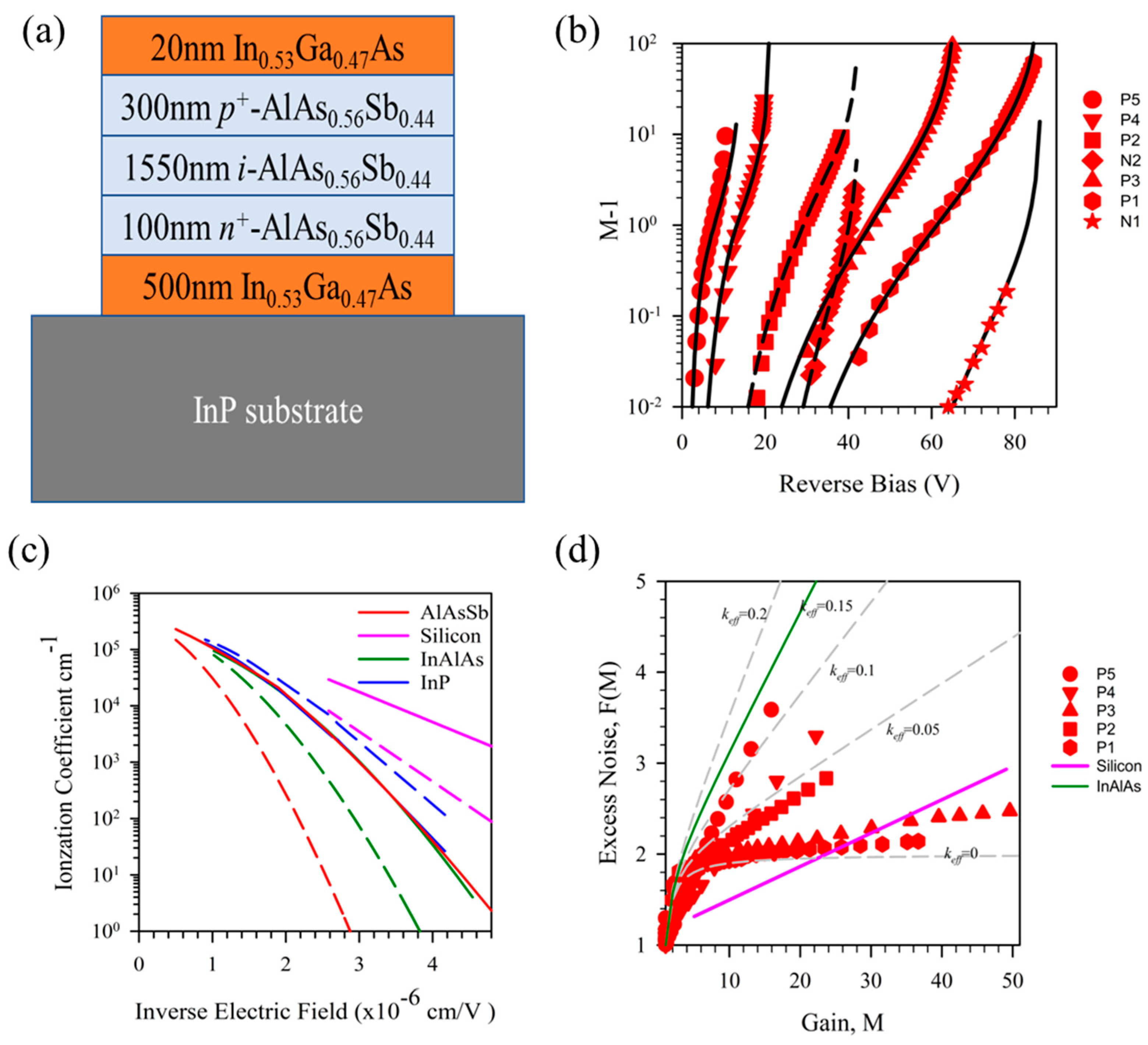
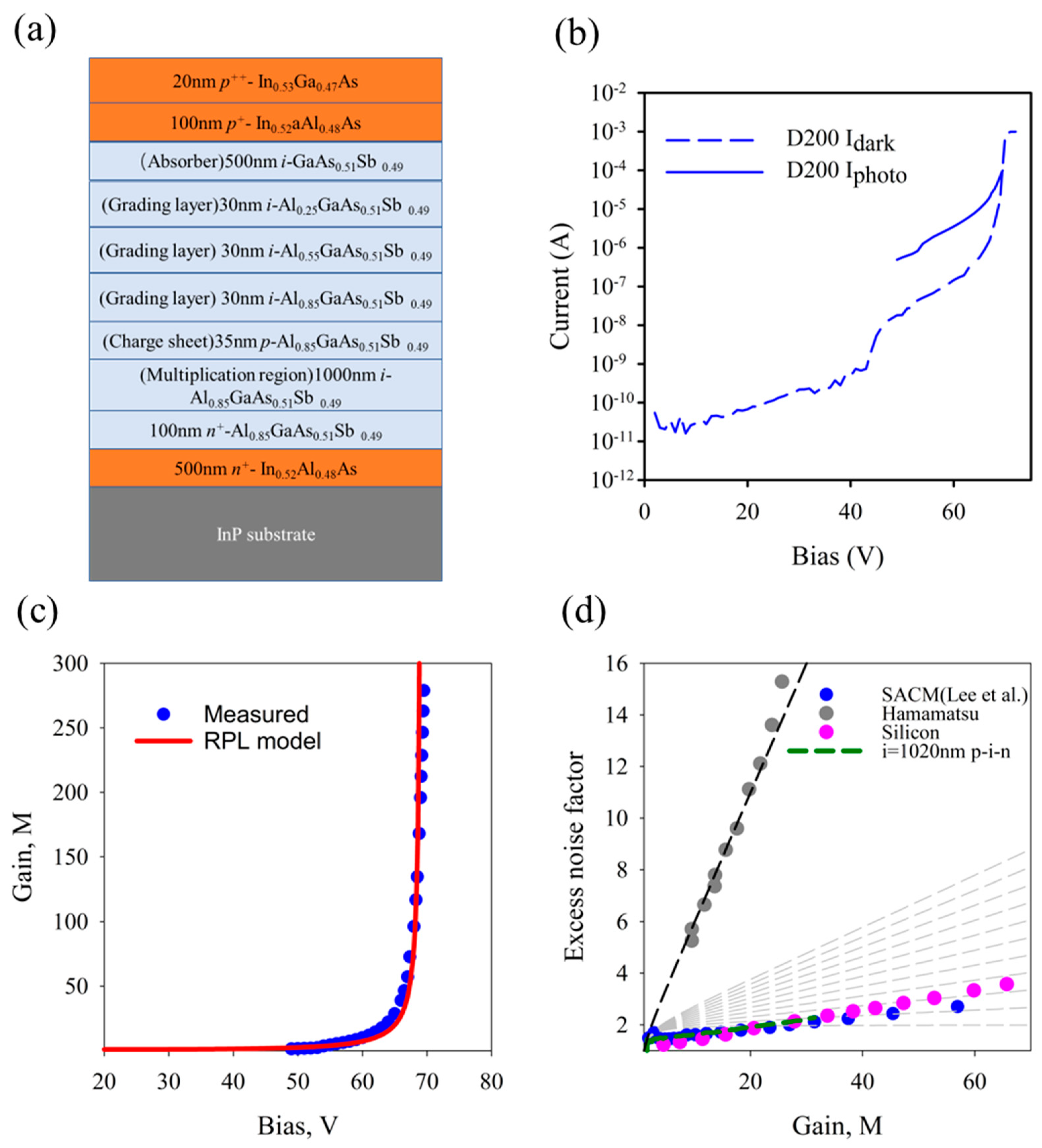
3.4. AlxGa1-xAs0.56Sb0.44 p-i-n and n-i-p Structure APDs

Initial studies of the avalanche multiplication and excess noise properties of AlAs0.56Sb0.44 and AlxGa1-xAs0.56Sb0.44 diode structures on InP focused on thin avalanching structures (<250 nm) [38,39,40]. The first report of AlAs0.56Sb0.44 with a thick multiplication region of >1 μm was undertaken by Yi et al. [14] on a series of digital-alloy-grown p-i-n and n-i-p structures to achieve pure electron and hole injection.
Single carrier electron and hole multiplication measurements from different avalanching width structures are shown as M-1 on a log scale in Figure 11b. The avalanching widths are as follows: P1 (N1) = 1550 nm, P2 (N2) = 660 nm, P3 = 1150 nm, P4 = 230 nm, and P5 = 80 nm. The InP substrates were semi-insulating and the “i” regions were unintentionally doped. The background carrier concentration was mid-1015 cm−3 n-type. From these multiplication characteristics, the ionization coefficients were extracted and these were found to be significantly larger than most III-V semiconductors and even silicon [14] as shown in Figure 11c. Excess noise measurements were undertaken using the noise measurement circuit developed by Lau et al. [41] on these thicker structures as shown in Figure 11d.
Following this, the avalanche multiplication and excess noise behavior of nominally 1 μm thick Al0.85Ga0.15As0.56Sb0.44 p-i-n structures were investigated by Lee et al. [16,17]. These structures grown by DA and RA techniques gave broadly similar multiplication (Figure 12a) and excess noise characteristics (Figure 12b) when differences in the layer thicknesses and background doping were corrected for. Taylor-Mew et al. [42] investigated the multiplication and excess noise in a nominally 600 nm thick avalanching structure and found that they could obtain an excess noise factor of 2.2 at a multiplication of 30.

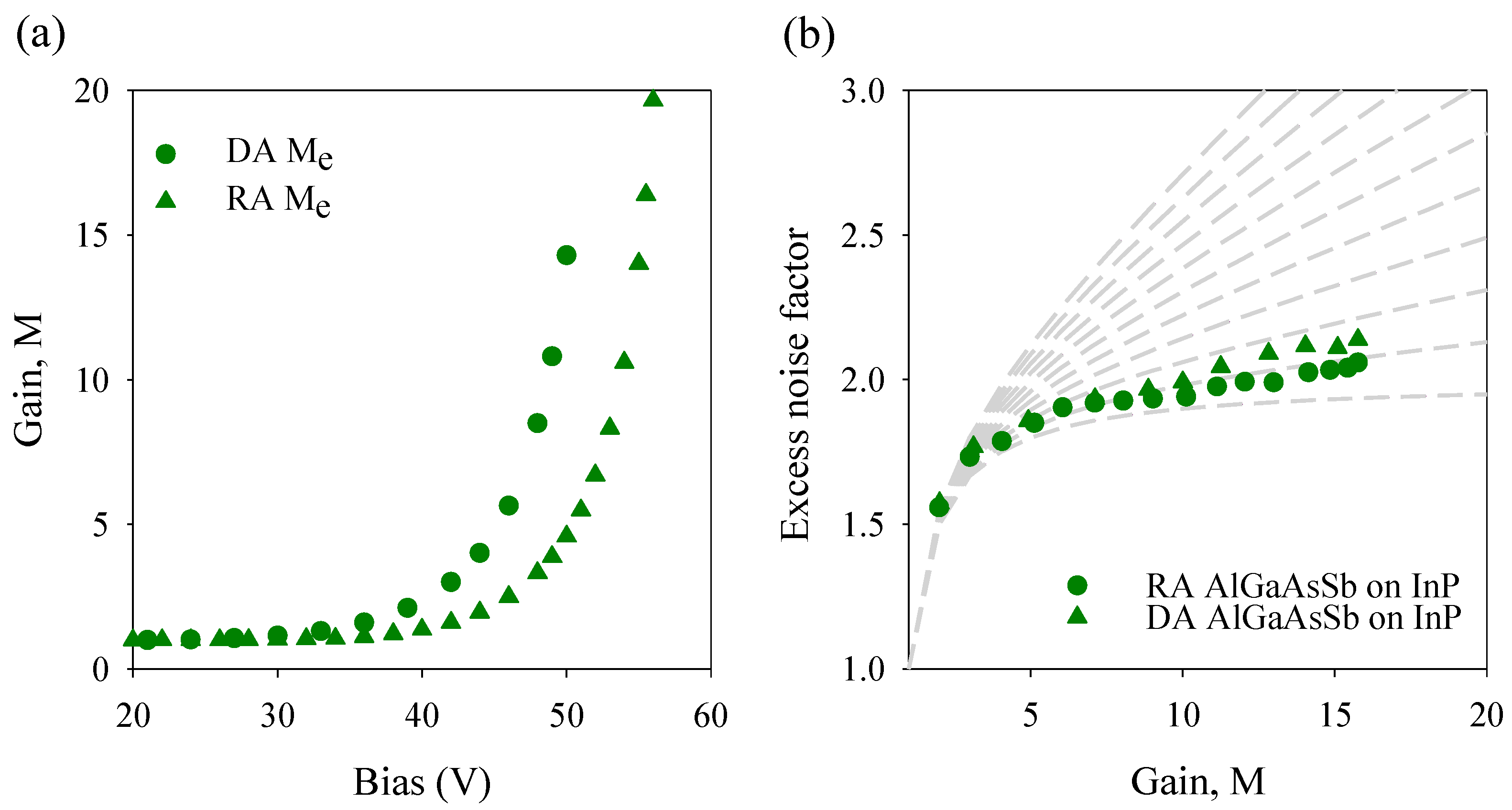
3.5. AlxGa1-xAs0.56Sb0.44 Separate Absorption, Charge, and Multiplication APDs

The AlxGa1-xAs0.56Sb0.44 alloys investigated so far have relatively large bandgaps and as such are not suitable for detecting longer wavelengths that are of interest for SWIR applications. Using a lower Al composition will reduce the bandgap, but this may give rise to high quantum mechanical tunneling dark currents at the high electric fields necessary for APD operation. As this material system is lattice-matched to InP, we can, however, use InGaAs or GaAs0.56Sb0.44 as the narrow-bandgap absorber material in a SACM structure with the avalanche multiplication occurring in the wider-bandgap AlxGa1-xAs0.56Sb0.44. Initial studies used InGaAs absorber regions and thin multiplication regions of AlAs0.56Sb0.44 [43] or Al0.85Ga0.15As0.56Sb0.44 [44]. While the temperature variation of the multiplication is reduced [35] and the APD speed improved [36] in these structures, the excess noise is only reduced primarily by the ‘dead-space’ effect rather than exploiting the large α/β ratio that is seen in thicker multiplication regions operating at lower electric fields. The first report of a SACM using a 1 μm thick multiplication region and a 500 nm thick GaAs0.56Sb0.44 absorber was by Lee et al. [45], as shown in Figure 13a. The current–voltage characteristics and gain versus bias voltage are shown in Figure 13b,c, respectively. Multiplication values of ~278 could be achieved with an F of 2.7 at M = 60, corresponding to a k = ~0.015 (Figure 13d). Additionally shown in Figure 13d is the excess noise of silicon and a Hamamatsu InGaAs APD device.
The speed performance of these Al0.85Ga0.15As0.56Sb0.44 APDs has been reported for the first time. A 200 µm diameter device has a −3 dB bandwidth of 0.7 GHz and a gain bandwidth product (GBP) of 11 at a reverse bias of 64 V. A similar structure with a thicker 885 nm GaAs0.56Sb0.44 absorber and a 200 nm thick Al0.85Ga0.15As0.56Sb0.44 multiplication region also demonstated a maximum multiplication of 180 but with a slightly higher noise of F = 2.48 at M = 20 [46], presumably due to the higher electric field in the multiplication region.

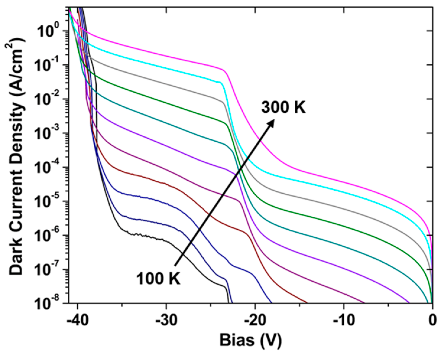
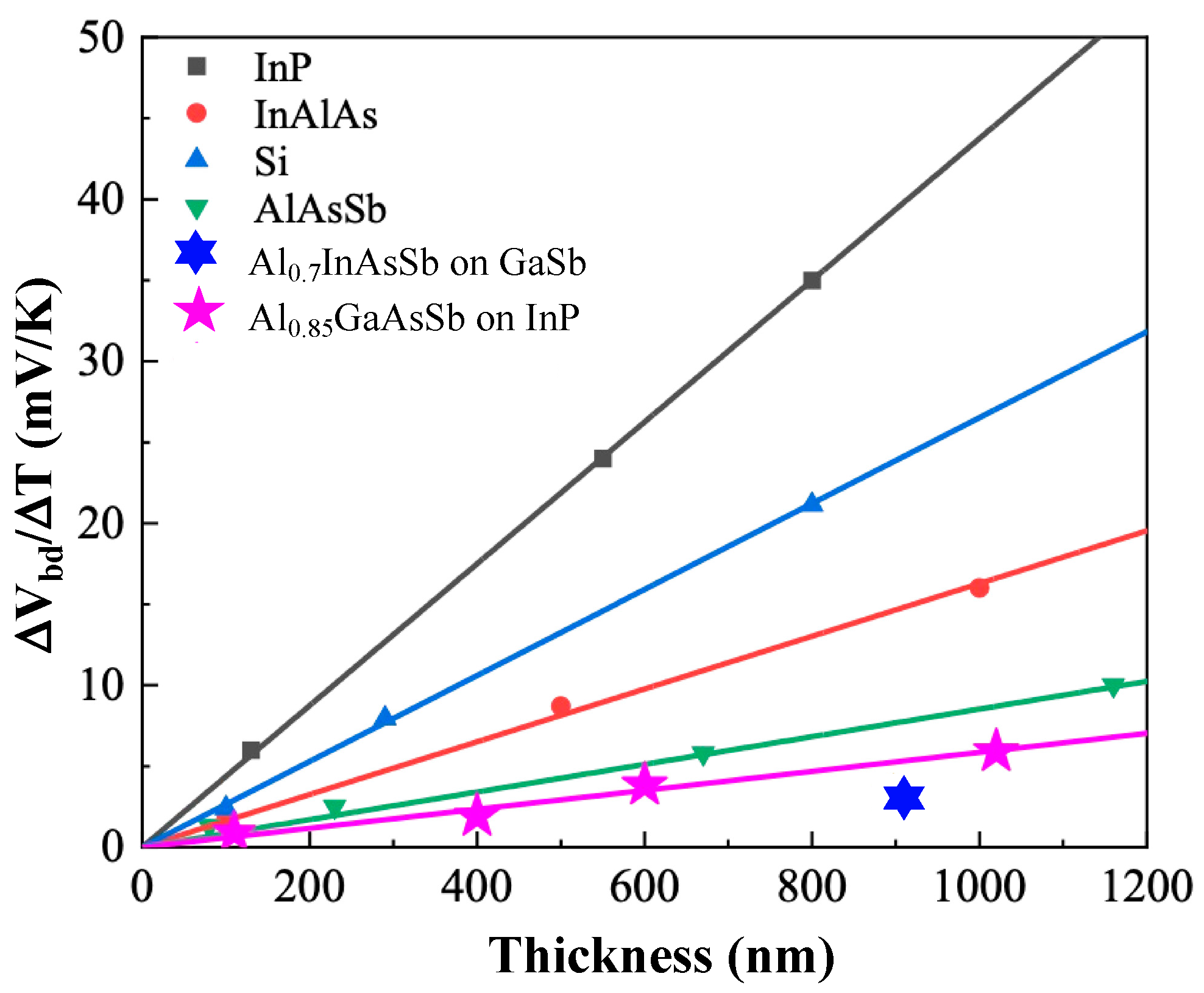
3.6. Temperature Variation of Breakdown Voltage

Typically, as carriers are accelerated by the electric field and gain sufficient energy to impact ionize, they also lose energy through scattering. Since phonons present one of the primary scattering mechanisms, the gain and, thus, the breakdown voltage vary with temperature. As a result, optical receivers that use APDs frequently require temperature stabilization of the detector chip, which adds cost and induces a power penalty. Reducing this limitation can simplify receiver design. Figure 14 shows the breakdown voltage temperature coefficient ΔVbd/ΔT versus multiplication layer thickness for AlxIn1-xAsySb1-y [47], InP [48], AlInAs [41], Si [49], and Al1-xGaxAsySb1-y [50,51]. The bandgap of random alloy and digital alloy AlInAsSb and random alloy AlGaAsSb was measured by the photoluminescence peak and external quantum efficiency versus temperature in the range 160 K to 300 K and found to exhibit weak temperature dependence. The weak temperature dependence of bandgap energy for these Sb-based quaternary alloys most likely arises from the weak electron–phonon coupling in these materials. It follows that the threshold energy for impact ionization should be relatively independent of temperature. Modeling supports that these quaternary alloys have high alloy scattering rates dominating phonon scattering mechanisms that reduce the temperature dependence of the avalanche breakdown. The origin of the weak temperature dependence of the quaternary Sb-based digital alloys is most likely due to the dominance of alloy scattering. In the Sb-based alloys, the large Sb and As nuclei difference creates large potential fluctuations that lead to higher disorder potential. Consequently, the resulting higher alloy scattering rate in these quaternary digital alloys is relatively independent of temperature. We conclude that phonon scattering is the dominant scattering mechanism in materials with high ΔVbd/ΔT, while alloy scattering is the dominant scattering mechanism in low ΔVbd/ΔT materials. The ΔVbd/ΔT of SACM-APD structures is larger than the ΔVbd/ΔT of just the multiplication region by the ratio of the total depletion width to the multiplication region width [40]. Jones et al. [39] found that the ΔVbd/ΔT of a 1 μm thick Al0.7InAsSb multiplication region with a 1 μm thick Al0.4InAsSb absorber SACM APD on GaSb was 15.8 mV/K. Later, the same group extended the detection wavelength to 2 μm by using a 1 μm thick Al0.3InAsSb absorber with a 0.5 μm thick Al0.7InAsSb multiplication region and obtained a ΔVbd/ΔT of ~13.5 mV/K [25]. Similarly, low values of ΔVbd/ΔT have been seen with Al0.85Ga0.15As0.56Sb0.44 SACM APDs on InP. Cao et al. [52] reported on a ΔVbd/ΔT of 4.31 mV/K in a SACM APD with a 1 μm thick GaAs0.56Sb0.44 absorber and a 200 nm thick Al0.85Ga0.15As0.56Sb0.44 multiplication region. More recently, Lee et al. [37] obtained a ΔVbd/ΔT of 11.8 mV/K in a SACM APD with a 0.5 μm thick GaAs0.56Sb0.44 absorber and a 1 μm thick Al0.85Ga0.15As0.56Sb0.44 multiplication region.

4. Discussion

Both of the wider-bandgap Sb-containing alloy systems of AlxIn1-xAsySb1-y on GaSb and AlxGa1-xAs0.56Sb0.44 on InP give rise to low-noise APDs. A large part of the low excess noise performance is because of the large difference between α and β in these materials. Figure 15 shows the ionization coefficients for AlxIn1-xAsySb1-y on GaSb, obtained from measurements of multiplication and excess noise by Yuan et al. [53], compared with those of InP and silicon. The ionization coefficients for Al0.85Ga0.15As0.56Sb0.44 were determined from a series of p-i-n and n-i-p structures of different thicknesses by Guo et al. [54] and are shown in Figure 15 together with the data for AlAsSb and silicon. In both alloy systems, the β is significantly lower than the α. For AlxIn1-xAsySb1-y, the β is ~10 times lower than the α while for AlxGa1-xAs0.56Sb0.44 the β is between 10 and 100 times lower, depending on the Al composition and the electric field. The α in Al0.85Ga0.15As0.56Sb0.44 is very similar to that of AlAsSb with the β being slightly larger. Nevertheless, the α/β ratio is still very large and compares favorably with silicon. Work performed by Liu et al. [55] on the ionization coefficients in GaAsBi alloys showed that the presence of the large Bi atom reduced β significantly but did not affect α much. This was attributed to the effect Bi has in increasing the split-off energy gap in the valence band, making it harder for holes to gain the energy to transfer to the split-off band and hence reducing their ionization transition rate. Sb is also a relatively large atom, and a similar increase to the split-off energy gap may explain why Sb-based alloys show reduced β values. The large α/β values seen in these alloys cannot fully explain the very low excess noise values seen in both these alloys, which are smaller than those predicted by the McIntyre k-values. This suggests that some other mechanism may be responsible for reducing the noise further. Recently, DS Ong et al. [56] suggested that the electron ionization probability distribution function (PDF) in AlAs0.56Sb0.44 has a narrow peak with a long tail, and that the hole ionization PDF was very broad. The shape of the PDFs follows a Weibull–Fréchet distribution than the more usual displaced exponential PDFs that are normally assumed. Using a Weibull–Fréchet-shaped PDF enabled the multiplication and excess noise in AlAs0.56Sb0.44 p-i-n diodes with avalanche widths of 660 nm to 1550 nm to be replicated accurately. The reason for this Weibull–Fréchet shape is presently unclear and will require a more detailed understanding of the band structure and the scattering processes at high fields in these Sb-based structures.
The Sb-based materials have demonstrated the potential to realize APDs with breakthrough performance. Over the past 50 years, there have been many efforts to develop APDs that can achieve multiplication noise as low as those fabricated from Si but that operate at the longer wavelengths required for applications such as optical communications, night-vision imaging, and, more recently, quantum information processing and transmission and LIDAR. AlInAsSb and AlGaAsSb now offer that capability for the SWIR and MWIR spectral regions. An added benefit for these materials is the relative insensitivity to changes in ambient temperature with potential savings in cost and a smaller component count in optical receivers. Since these are III-V compounds with high absorption coefficients and high carrier saturation velocities, they can also achieve much higher bandwidths than Si APDs in the near-infrared or HgCdTe in the MWIR.

Funding

Research by JCC and SRB was funded by the Army Research Office and DARPA (W911NF-17-1-0065); DARPA (W909MY-12-D-0008).

Institutional Review Board Statement

Not applicable.

Informed Consent Statement

Not applicable.

Data Availability Statement

Data underlying the results presented in this paper are not publicly available at this time but may be obtained from the authors upon reasonable request.

Acknowledgments

The authors thank Xiao Jin for assistance with the figures.

Conflicts of Interest

The authors declare no conflict of interest.

References

  1. Campbell, J.C. Advances in photodetectors. In Optical Fiber Telecommunications V; Kaminow, I., Li, T., Willner, A.E., Eds.; Elsevier: Amsterdam, The Netherlands, 2008; Volume A, pp. 221–268. [Google Scholar]
  2. Huang, Z.; Li, C.; Liang, D.; Yu, K.; Santori, C.; Fiorentino, M.; Sorin, W.; Palermo, S.; Beausoleil, R.G. 25 Gbps low-voltage waveguide Si–Ge avalanche photodiode. Optica 2016, 3, 793–798. [Google Scholar] [CrossRef]
  3. Lecomte, R.; Martel, C.; Carrier, C. Status of BGO-avalanche photodiode detectors for spectroscopic and timing measurements. Nucl. Instrum. Methods Phys. Res. Sect. Accel. Spectrometers Detect. Assoc. Equip. 1989, 278, 585–597. [Google Scholar] [CrossRef]
  4. Dunai, D.; Zoletnik, S.; Sárközi, J.; Field, A.R. Avalanche photodiode based detector for beam emission spectroscopy. Rev. Sci. Instrum. 2010, 81, 103503. [Google Scholar] [CrossRef] [Green Version]
  5. Albota, M.A.; Heinrichs, R.M.; Kocher, D.G.; Fouche, D.G.; Player, B.E.; O’Brien, M.E.; Aull, B.F.; Zayhowski, J.J.; Mooney, J.; Willard, B.C.; et al. Three-dimensional imaging laser radar with a photon-counting avalanche photodiode array and microchip laser. Appl. Opt. 2002, 41, 7671–7678. [Google Scholar] [CrossRef] [PubMed] [Green Version]
  6. Brian, F.; Aull, B.F.; Duerr, E.K.; Frechette, J.P.; McIntosh, K.A.; Schuette, D.R.; Younger, R.D. Large-Format Geiger-Mode Avalanche Photodiode Arrays and Readout Circuits. IEEE J. Sel. Top. Quantum. Electron. 2018, 24, 1–10. [Google Scholar]
  7. Hugi, A.; Villares, G.; Blaser, S.; Liu, H.C.; Faist, J. Mid-infrared frequency comb based on a quantum cascade laser. Nature 2021, 492, 229–233. [Google Scholar] [CrossRef]
  8. Villares, G.; Hugi, A.; Blaser, S.; Faist, J. Dual-comb spectroscopy based on quantum-cascade-laser frequency combs. Nat. Commun. 2014, 5, 5192. [Google Scholar] [CrossRef] [Green Version]
  9. Jiang, X.; Itzler, M.; O’Donnell, K.; Entwistle, M.; Owens, M.; Slomkowski, K.; Rangwala, S. InP-Based Single-Photon Detectors and Geiger-Mode APD Arrays for Quantum Communications Applications. IEEE J. Sel. Top. Quantum Electron. 2015, 21, 5–16. [Google Scholar] [CrossRef]
  10. Kardynał, B.E.; Yuan, Z.L.; Shields, A.J. An avalanche-photodiode-based photon-number-resolving detector. Nat. Photonics 2008, 2, 425–428. [Google Scholar] [CrossRef] [Green Version]
  11. McIntyre, R.J. Multiplication noise in uniform avalanche diodes. IEEE Trans. Electron. Dev. 1966, 13, 154–158. [Google Scholar] [CrossRef]
  12. Vaughn, L.G.; Dawson, L.R.; Pease, E.A.; Lester, L.F.; Xu, H.; Jiang, Y.; Gray, A.L. Type I mid-infrared MQW lasers using AlInAsSb barriers and InAsSb wells. Proc. SPIE 2005, 5722, 307–318. [Google Scholar]
  13. Maddox, S.J.; Bank, S.R. Broadly Tunable AlInAsSb Digital Alloys Grown on GaSb. ACS Cryst. Growth Des. 2016, 16, 3582–3586. [Google Scholar] [CrossRef]
  14. Yi, X.; Xie, S.; Liang, B.; Lim, L.W.; Zhou, X.; Debnath, M.C.; Huffaker, D.L.; Tan, C.H.; David, J.P.R. Demonstration of large ionization coefficient ratio in AlAs0.56Sb0.44 lattice matched to InP. Sci. Rep. 2018, 8, 8–13. [Google Scholar] [CrossRef] [PubMed]
  15. Yi, X.; Xie, S.; Liang, B.; Lim, L.W.; Cheong, J.S.; Debnath, M.C.; Huffaker, D.L.; Tan, C.H.; David, J.P.R. Extremely low excess noise and high sensitivity AlAs0.56Sb0.44 avalanche photodiodes. Nat. Photonics 2019, 13, 683–686. [Google Scholar] [CrossRef]
  16. Lee, S.; Kodati, S.H.; Guo, B.; Jones, A.H.; Schwartz, M.; Winslow, M.; Grein, C.H.; Ronningen, T.J.; Campbell, J.C.; Krishna, S. Low noise Al0.85Ga0.15As0.56Sb0.44 avalanche photodiodes on InP substrates. Appl. Phys. Lett. 2021, 118, 081106. [Google Scholar] [CrossRef]
  17. Lee, S.; Guo, B.; Kodati, S.H.; Jung, H.; Schwartz, M.; Jones, A.H.; Winslow, M.; Grein, C.H.; Ronningen, T.J.; Campbell, J.C.; et al. Random alloy thick AlGaAsSb avalanche photodiodes on InP substrates. Appl. Phys. Lett. 2022, 120, 071101. [Google Scholar] [CrossRef]
  18. Ren, M.; Maddox, S.J.; Woodson, M.E.; Chen, Y.; Bank, S.R.; Campbell, J.C. Characteristics of AlxIn1−xAsySb1−y (x: 0.3–0.7) avalanche photodiodes. IEEE J. Light. Tech. 2017, 35, 2380–2384. [Google Scholar] [CrossRef]
  19. Woods, M.H.; Johnson, W.C.; Lampert, M.A. Use of a Schottky barrier to measure impact ionization coefficients in semiconductors. Solid-State Electron. 1973, 16, 381–394. [Google Scholar] [CrossRef]
  20. Kodati, S.H.; Lee, S.; Guo, B.; Jones, A.H.; Schwartz, M.; Winslow, M.; Pfiester, N.A.; Grein, C.H.; Ronningen, T.J.; Campbell, J.C.; et al. AlInAsSb avalanche photodiodes on InP substrates. Appl. Phys. Lett. 2012, 118, 091101. [Google Scholar] [CrossRef]
  21. Ahmed, S.Z.; Tan, Y.; Zheng, J.; Campbell, J.C.; Ghosh, A.W. Atomistic Transport Modeling, Design Principles, and Empirical Rules for Low-Noise III-V Digital-Alloy Avalanche Photodiodes. Phys. Rev. Appl. 2022, 17, 034044. [Google Scholar] [CrossRef]
  22. Kang, Y.; Liu, H.-D.; Morse, M.; Paniccia, M.J.; Zadka, M.; Litski, S.; Sarid, G.; Pauchard, A.; Kuo, Y.-H.; Chen, H.-W.; et al. Epitaxially-Grown Ge/Si Avalanche Photodiodes for 1.3 mm Light Detection. Nat. Photonics 2009, 3, 59. [Google Scholar] [CrossRef]
  23. Huang, M.; Cai, P.; Wang, L.; Shi, T.; Chen, W.; Li, S.; Hou, G.; Hong, C.; Pan, D. Development of Si photonics technology: Ge/Si avalanche photodiode for PON applications. In Proceedings of the Optical Fiber Communication Conference, San Francisco, CA, USA, 9–13 March 2014. [Google Scholar]
  24. Nada, M.; Muramoto, Y.; Yokoyama, H.; Toshimatsu, T.; Matsuzaki, H. High-speed avalanche photodiodes for 100-Gb/s systems and beyond. In Proceedings of the European Conference on Optical Communications, Cannes, France, 21–25 September 2014. [Google Scholar]
  25. Jones, A.H.; March, S.D.; Bank, S.R.; Campbell, J.C. AlInAsSb/GaSb Separate Absorption, Charge, and Multiplication Avalanche Photodiodes for 2-μm Applications. Nat. Photonics 2020, 14, 559–563. [Google Scholar] [CrossRef]
  26. Zheng, J.; Jones, A.H.; Tan, Y.; Rockwell, A.K.; March, S.; Ahmed, S.Z.; Dukes, C.A.; Ghosh, A.W.; Bank, S.R.; Campbell, J.C. Characterization of band offsets in AlxIn1−xAsySb1−y alloys with varying Al composition. Appl. Phys. Lett. 2019, 115, 122105. [Google Scholar] [CrossRef]
  27. Jones, A.H.; March, S.D.; Dadey, A.A.; Muhowski, A.J.; Bank, S.R.; Campbell, J.C. AlInAsSb Separate Absorption, Charge, and Multiplication Avalanche Photodiodes for Mid-Infrared Detection. IEEE J. Quantum. Electron. 2022, 58, 4500306. [Google Scholar] [CrossRef]
  28. Maddox, S.J.; Sun, W.; Lu, Z.; Nair, H.P.; Campbell, J.C.; Bank, S.R. Enhanced low-noise gain from InAs avalanche photodiodes with reduced dark current and background doping. Appl. Phys. Lett. 2012, 101, 151124. [Google Scholar] [CrossRef] [Green Version]
  29. Ker, P.J.; Marshall, A.R.J.; Krysa, A.B.; David, J.P.R.; Tan, C.H. Temperature Dependence of Leakage Current in InAs Avalanche Photodiodes. IEEE J. Quantum. Electron. 2011, 47, 1123–1128. [Google Scholar] [CrossRef]
  30. Dadey, A.A.; McArthur, J.A.; Kamboj, A.; Bank, S.R.; Wasserman, D.; Campbell, J.C. High-gain low-excess-noise MWIR detection with a 3.5-μm cutoff AlInAsSb-based separate absorption, charge, and multiplication avalanche photodiode. APL Photonics 2023, 8, 036101. [Google Scholar] [CrossRef]
  31. Rothman, J.; Perrais, G.; Destefanis, G.; Baylet, J.; Castelein, P.; Chamonal, J.-P. High performance characteristics in pin MW HgCdTe e-APDs. Proc. SPIE 2007, 6542, 475–484. [Google Scholar]
  32. Singh, A.; Srivastav, V.; Pal, R. HgCdTe avalanche photodiodes: A review. Opt. Laser Tech. 2011, 43, 1358. [Google Scholar] [CrossRef]
  33. Sun, W.; Lu, Z.; Zheng, X.; Campbell, J.C.; Maddox, S.J.; Nair, H.P.; Bank, S.R. High gain InAs avalanche photodiodes. IEEE J. Quantum. Electron. 2013, 49, 154–161. [Google Scholar] [CrossRef] [Green Version]
  34. Marshall, R.J.; Tan, C.H.; Steer, M.J.; David, J.P.R. Extremely Low Excess Noise in InAs Electron Avalanche Photodiodes. IEEE Photon. Technol. Lett. 2009, 21, 866–868. [Google Scholar] [CrossRef] [Green Version]
  35. Huang, J.; Zhao, C.; Zhao, C.; Nie, B.; Xie, S.; Kwan, D.C.M.; Meng, X.; Zhang, Y.; Huffaker, D.L.; Ma, W. High-performance mid-wavelength InAs avalanche photodiode using AlAs0.13Sb0.87 as the multiplication layer. Photon. Res. 2020, 8, 755–759. [Google Scholar] [CrossRef]
  36. Capasso, F.; Tsang, W.T.; Williams, G.F. Staircase solid-state photomultipliers and avalanche photodiodes with enhanced ionization rates ratio. IEEE Trans. Electron. Dev. 1983, 30, 381–390. [Google Scholar] [CrossRef]
  37. March, S.D.; Jones, A.H.; Campbell, J.C.; Bank, S.R. Multistep staircase avalanche photodiodes with extremely low noise and deterministic amplification. Nat. Photonics 2021, 15, 468–474. [Google Scholar] [CrossRef]
  38. Xie, S.; Tan, C.H. AlAsSb avalanche photodiodes with a Sub-mV/K temperature coefficient of breakdown voltage. IEEE J. Quantum. Electron. 2011, 47, 1391–1395. [Google Scholar]
  39. Xie, J.; Xie, S.; Tozer, R.C.; Tan, C.H. Excess noise characteristics of thin AlAsSb APDs. IEEE Trans. Electron. Dev. 2012, 59, 1475–1479. [Google Scholar] [CrossRef]
  40. Zhou, X.; Zhang, S.; David, J.P.R.; Ng, J.S.; Tan, C.H. Avalanche Breakdown Characteristics of Al1−xGaxAs0.56Sb0.44 Quaternary Alloys. IEEE Photon. Technol. Lett. 2016, 28, 2495–2498. [Google Scholar] [CrossRef] [Green Version]
  41. Lau, K.S.; Ng, B.K.; Li, K.F.; Tan, C.H. Excess noise measurement in avalanche photodiodes using a transimpedance amplifier front-end. Meas. Sci. Technol. 2016, 17, 1941–1946. [Google Scholar] [CrossRef]
  42. Taylor-Mew, J.; Shulyak, V.; White, B.; Tan, C.H.; Ng, J.S. Low Excess Noise of Al0.85Ga0.15As0.56Sb0.44Avalanche Photodiode from Pure Electron Injection. IEEE Photonics Technol. Lett. 2021, 33, 1155–1158. [Google Scholar] [CrossRef]
  43. Tan, C.H.; Xie, S.; Xie, J. Low Noise Avalanche Photodiodes Incorporating a 40 nm AlAsSb Avalanche Region. IEEE J. Quantum. Electron. 2012, 48, 36–41. [Google Scholar] [CrossRef]
  44. Xie, S.; Zhou, X.; Zhang, S.; Thomson, D.J.; Chen, X.; Reed, G.T.; Ng, J.S.; Tan, C.H. InGaAs/AlGaAsSb avalanche photodiode with high gain-bandwidth product. Opt. Exp. 2016, 24, 24242. [Google Scholar] [CrossRef]
  45. Lee, S.; Jin, X.; Jung, H.; Lewis, H.; Liu, Y.; Guo, B.; Kodati, S.H.; Schwartz, M.; Grein, C.; Ronningen, T.J.; et al. High Gain, Low Noise, Room Temperature 1550 nm GaAsSb/AlGaAsSb Avalanche Photodiodes. Optica 2022, 10, 147–154. [Google Scholar] [CrossRef]
  46. Cao, Y.; Blain, T.; Taylor-Mew, J.D.; Li, L.; Ng, J.S.; Tan, C.H. Extremely low excess noise avalanche photodiode with GaAsSb absorption region and AlGaAsSb avalanche region. Appl. Phys. Lett. 2023, 122, 51103. [Google Scholar] [CrossRef]
  47. Jones, A.H.; Yuan, Y.; Ren, M.; Woodson, M.; Maddox, S.; Bank, S.; Campbell, J.C. AlxIn1−xAsySb1−y photodiodes with low avalanche breakdown temperature dependenc. Opt. Express 2017, 25, 24340–24345. [Google Scholar] [CrossRef] [PubMed] [Green Version]
  48. Tan, L.J.J.; Ong, D.S.G.; Ng, J.-S.; Hing Tan, C.H.; Jones, S.K.; Qian, Y.; David, J.P.R. Temperature dependence of avalanche breakdown in InP and InAlAs. IEEE J. Quantum Electron. 2010, 46, 1153–1157. [Google Scholar] [CrossRef]
  49. Massey, D.J.; David, J.P.R.; Rees, G.J. Temperature dependence of impact ionization in submicrometer silicon devices. IEEE Trans. Electron Devices 2006, 53, 2328–2334. [Google Scholar] [CrossRef]
  50. Guo, B.; Ahmed, S.Z.; Xue, X.; Rockwell, A.K.; Ha, J.; Lee, S.; Liang, B.; Jones, A.H.; McArthur, J.A.; Kodati, S.H.; et al. Temperature Dependence of Avalanche Breakdown of AlGaAsSb and AlInAsSb Avalanche Photodiodes. IEEE J. Light. Technol. 2022, 40, 5934–5942. [Google Scholar] [CrossRef]
  51. Jin, X.; Xie, S.; Liang, B.; Yi, X.; Lewis, H.; Lim, L.W.; Liu, Y.; Ng, B.K.; Huffaker, D.L.; Tan, C.H.; et al. Temperature Dependence of the Impact Ionization Coefficients in AlAsSb Lattice Matched to InP. IEEE J. Sel. Top. Quantum. Electron. 2022, 28, 3801208. [Google Scholar] [CrossRef]
  52. Cao, Y.; Osman, T.; Clarke, E.; Patil, P.K.; Ng, J.S.; Tan, C.H. A GaAsSb/AlGaAsSb Avalanche Photodiode With a Very Small Temperature Coefficient of Breakdown Voltage. IEEE J. Light. Tech. 2022, 14, 4709–4713. [Google Scholar] [CrossRef]
  53. Yuan, Y.; Zheng, J.; Rockwell, A.K.; March, S.D.; Bank, S.R.; Campbell, J.C. AlInAsSb Impact Ionization Coefficients. IEEE Photon. Tech. Lett. 2019, 31, 315–318. [Google Scholar] [CrossRef]
  54. Guo, B.; Jin, X.; Lee, S.; Ahmed, S.Z.; Jones, A.H.; Xue, X.; Liang, B.; Lewis, H.; Kodati, S.; Chen, D.; et al. Impact ionization coefficients of digital alloy and random alloy Al0.85Ga0.15As0.56Sb0.44 in a wide electric field range. IEEE J. Light. Tech. 2022, 40, 4758–4764. [Google Scholar] [CrossRef]
  55. Liu, Y.; Yi, X.; Bailey, N.J.; Zhou, Z.; Rockett, T.B.O.; Lim, L.W.; Tan, C.H.; Richards, R.D.; David, J.P.R. Valence band engineering of GaAsBi for low noise avalanche photodiodes. Nature Comm. 2021, 12, 1–8. [Google Scholar] [CrossRef] [PubMed]
  56. Ong, D.S.; Tan, A.H.; Choo, K.Y.; Yeoh, K.H.; David, J.P.R. Weibull-Fréchet random path length model for avalanche gain and noise in photodiodes. J. Phys. D. Appl. Phys. 2022, 55, 065105. [Google Scholar] [CrossRef]
Figure 1. Variation in bandgap energy of AlxIn1-xAsySb1-y lattice-matched to GaSb versus Al concentration.
Photonics 10 00715 g001
Figure 2. Schematic cross-section of p-i-n structure AlxIn1-xAsySb1-y APDs.
Photonics 10 00715 g002
Figure 3. Dark current density of x = 0.7, 0.3, and 0.15 AlxInAsSb photodiodes.
Photonics 10 00715 g003
Figure 4. Excess noise factor of an Al0.7InAsSb APD and a Si APD versus gain for illumination at 445 nm.
Photonics 10 00715 g004
Figure 5. Schematic cross-section of an AlxInAsSb SACM APD. The multiplication layer has x = 0.7. The graph on the right shows the magnitude of the electric field in each region. The substrate is GaSb.
Photonics 10 00715 g005
Figure 6. Dark current, photocurrent, and measured and simulated () gain versus reverse bias of a 50 µm diameter AlxIn1-xAsySb1-y SACM APD at 300 K [25].
Photonics 10 00715 g006
Figure 7. The energy band diagram of the p-compensated absorber simulated at the indicated reverse biases [27].
Photonics 10 00715 g007
Figure 8. The dark current density of the p-compensated design as a function of temperature. Each curve represents a 20 K increment from 100 to 300 K as indicated [27].
Photonics 10 00715 g008
Figure 9. Band diagram and illustration of localized impact ionization of a staircase APD under reverse bias.
Photonics 10 00715 g009
Figure 10. The measured excess noise factor for a 2- and 3-step staircase compared to the theoretical excess noise for a staircase APD.
Photonics 10 00715 g010
Figure 11. (a) shows a layer schematic of the p-i-n structure P1; (b) shows the measured multiplication in a series of p-i-n and n-i-p structures plotted as M-1; (c) the ionization coefficients of AlAs0.56Sb0.44 compared to that of InP, InAlAs, and silicon (solid lines are α and dashed lies are β); (d) measured excess noise of P1-P5 with electron-initiated multiplication. Additionally shown is the excess noise of InAlAs and silicon.
Photonics 10 00715 g011
Figure 12. (a) shows the electron-initiated multiplication from two nominally 1 μm DA and RA grown Al0.85Ga0.15As0.56Sb0.44 p-i-n structures; (b) the excess noise for the same layers as in (a).
Photonics 10 00715 g012
Figure 13. (a) Schematic of the SACM GaAs0.56Sb0.44/Al0.85Ga0.15As0.56Sb0.44 APD; (b) the bias dependence of dark current and photocurrent in a 200 μm diameter device; (c) the measured multiplication (symbols) and the calculated multiplication (line) for the APD; (d) the measured excess noise for this APD compared with results of a silicon APD and a Hamamatsu InGaAs APD.
Photonics 10 00715 g013
Figure 14. Comparison of the temperature coefficient of breakdown voltage of InP, InAlAs, Si, AlAsSb, Al0.85GaAsSb lattice-matched to InP, and AlxIn1-xAsySb1-y lattice-matched to GaSb. Symbols are measured values, and solid lines are linear fits.
Photonics 10 00715 g014
Figure 15. Impact ionization coefficients for AlxIn1-xAsySb1-y on GaAs (blue) and Al0As0.56Sb0.44 (red) and Al0.85Ga0.15As0.56Sb0.44 (green) on InP. The α in Al0.85Ga0.15As0.56Sb0.44 overlaps that of Al0As0.56Sb0.44 except in high fields. Data for silicon are also shown as a reference. Solid lines are α and dashed lines are β.
Photonics 10 00715 g015
Table 1. The 3.5 μm cutoff SACM APD compared to other MWIR APDs.
Ref.MaterialOperating Temperature (K)Maximum GainGain Normalized DCD (MA/cm2)Cutoff Wavelength (µm)
[30]Al0.05InAsSb1008500.05~3.5
[34]InAs77270.005~3
[35]InAs2003300.4~3.2
[27]Al0.15InAsSb1003806.0~2.9
[31]HgCdTe7753000.001~5
Disclaimer/Publisher’s Note: The statements, opinions and data contained in all publications are solely those of the individual author(s) and contributor(s) and not of MDPI and/or the editor(s). MDPI and/or the editor(s) disclaim responsibility for any injury to people or property resulting from any ideas, methods, instructions or products referred to in the content.

