1. Introduction
High-efficiency solid-state sensitized photovoltaic technology is emerging as a promising and cost-effective contender for harvesting solar power as a renewable source of energy. Recently, organic-inorganic hybrid perovskites, CH
3NH
3PbX
3 (X is iodine or a mixture of iodine and chlorine), have been intensively pursued as solid-state sensitizers for the traditional dye-sensitized solar cells to planar-heterojunction solar cells [
1,
2,
3]. This class of materials possesses several advantages, such as a direct band gap of approximately 1.55 eV, a high absorption coefficient, high electron mobility, and solution processability. In a typical perovskite solar cell, the absorber layer, with a thickness of several hundred nanometers, is sandwiched between the electron-transport layer (ETL) and the hole-transport layer (HTL) to enhance its photoactive properties [
4,
5].
Thermal vacuum evaporation is the most promising of the numerous methods for direct deposition of perovskite layers on dielectric or silicon substrates. Using this method, it is possible to obtain evenly and uniformly perovskite layers that compactly cover even nano- or microtextured surfaces of the substrates [
1,
6]. In addition, this process avoids the use of toxic solvents. Vacuum evaporation of perovskite layers is carried out in two ways, namely, sequentially (layer-by-layer) and jointly (co-evaporated) [
4,
7]. In the case of co-evaporation, the sublimation of the initial organic and inorganic materials (precursors) of perovskite is carried out in a vacuum chamber simultaneously. In sequential evaporation, the inorganic precursor is deposited first, followed by the organic precursor. It should be noted that the first technique does not require a post-annealing step, but in the second case, post-annealing is required to achieve complete conversion of precursors into perovskite. From this point of view, the most promising is the co-evaporation method.
In this work, we propose to use a sol–gel layer of strontium titanate (SrTiO
3) doped with niobium (Nb) ions in various concentrations as an ETL. Along with other techniques, the sol–gel method allows the synthesis of materials with different functional properties [
8,
9,
10,
11,
12]. SrTiO
3, a widely used substrate material for electronic oxide thin-film devices, has many interesting features. It is a dielectric with a cubic perovskite structure and a wide bandwidth of about 3.2 eV at 300 K in the stoichiometric composition. The transparency and dielectric properties of SrTiO
3 have made it one of the most commonly used single-crystal substrates for electronic oxide thin-film devices. SrTiO
3 also obtains a certain interest in condensed matter physics due to its conductive phases, low and high resistance switching [
13,
14,
15], photocurrent [
16,
17,
18], and other properties.
An outstanding feature of SrTiO
3 bulk material and thin films on its base is the ability to control its characteristics by choosing the synthesis method and changing its parameters. The properties of SrTiO
3 have been investigated for many years, including its electronic characteristics upon doping [
19,
20,
21,
22]. Oxygen vacancies induce free electrons with unusually high mobility for such a narrow-band system, with significant charged-impurity screening provided by the lattice. Recently, the SrTiO
3 thin sol–gel film has been actively investigated in order to utilize this wide range of physical properties as a prominent sublayer for many perovskite structures.
In this study, we combine the sol–gel method of synthesis of the niobium-doped SrTiO3 layer (SrTiO3:xNb) with the vacuum co-evaporation technique of the perovskites deposition.
2. Experimental
2.1. Sol–Gel Synthesis of SrTiO3:xNb Films
The sol–gel method was used in the present work to synthesize SrTiO3:xNb thin layers with different ratios of Nb (x = 0; 0.03; 0.06). Three types of sol have been prepared for the synthesis of film structures. For the synthesis of strontium titanate sol (sol I), titanium isopropoxide (Ti(OC3H7)4) (97%, Sigma–Aldrich, Steinheim, Germany), strontium acetate Sr(CH3CHOO)2 (ACS reagent 98%, Sigma-Aldrich, Steinheim, Germany), 2-Methoxyethanol (CH3OCH2CH2OH) (ACS reagent 98%, Sigma–Aldrich, Steinheim, Germany), isopropanol (CH3CH(OH)CH3) (ACS reagent 98%, Sigma–Aldrich, Steinheim, Germany), and acetic acid (CH3COOH) were used. The amounts of titanium isopropoxide and strontium acetate have been chosen so that the Ti/Sr ratio corresponds to the stoichiometric composition of strontium titanate in the films. The solution was stirred with an electromechanical stirrer for 1 h until all components had been completely dissolved, resulting in the formation of a stable film-forming sol. Sol II was prepared according to the following technique. For the synthesis of SrTiO3:(Nb) layers with different concentrations of niobium, NbCl5 (ACS 98% reagent, Sigma–Aldrich, Steinheim, Germany) has been used at concentrations of 0.03 and 0.06. Two solutions were prepared. The solution based on titanium isopropoxide (Ti(OC3H7)4) (97%, Sigma-Aldrich, Steinheim, Germany) in 2-Methoxyethanol (CH3OCH2CH2OH) (ACS reagent 98%, Sigma–Aldrich, Steinheim, Germany) was stirred until cool. Separately, niobium pentachloride (ACS reagent 98%, Sigma–Aldrich, Steinheim, Germany) has been dissolved in acetic acid (CH3COOH) and stirred until complete dissolution. Finally, the titanium and strontium isopropoxide solutions were mixed and stirred for about 5 min. Isopropanol (CH3CH(OH)CH3) and 2-Methoxyethanol (CH3OCH2CH2OH) have been added to this solution, which was then further stirred for 1.5 h. Before precipitation, the sol must be kept for at least 24 h in sealed conditions. Samples representing layers of SrTiO3 and SrTiO3:Nb were obtained by deposition, in which sols were deposited onto the substrate by the spin-coating technique. During the deposition of the strontium titanate sol–gel film, part of the silicon wafer remained accessible for further contact formation. The p-type 400 m-thick crystalline silicon (100) wafers with a resistivity of 3.0 Ω cm were used as the initial experimental substrates. The fixed substrate was spun up to 3000 rpm. Then the required number of layers has been applied (3 layers). After application of sol I or sol II, it was dried at 200 °C for 10 min. The next step is annealing. We place the substrate with the applied sol in the muffle furnace. Interlayer annealing occurs at a temperature of 250 °C and a holding time of 5 min. The final annealing has been carried out at a temperature of 500 °C and a holding time of 60 min.
2.2. Preparation of Perovskite Layers
In this study, we used a Cl-doped mixed-halide CH
3NH
3PbI
3−xCl
x perovskite as an active photoabsorber, which is characterized by low production cost, good stability, and relatively low toxicity [
1,
2,
3,
4]. The perovskite layer was deposited by the vacuum co-evaporation technique in a VUP-4 chamber using inorganic lead iodide (PbI
2) and organic methylammonium chloride (CH
3NH
3Cl or MACl) as the raw precursors. It is known that the problem of large-scale use of perovskite-based solar cells is instability since the properties of the perovskite layers gradually change during long-term storage in the air under the influence of the environment (humidity, temperature, UV radiation). We added 2.3% cesium iodide to the PbI
2 precursor during evaporation to improve stability. As shown in Ref. [
23], in this case, under normal storage conditions, the properties of perovskite layers do not change for a long time (test duration: 180 days). In addition, it should be taken into account that appropriate solar cell encapsulation also contributes to increasing the stability of the perovskite layers during operation.
During the experiments, the following optimal mode of the deposition process was chosen. At a precursor composition of 4:1 (MACl:PbI
2) and a process pressure of 1.3 × 10
−5 mbar, the deposition rate of the MACl was maintained at a level of 1.2 Å/s, while that of the PbI
2 was kept at 0.4 Å/s. The temperatures of the crucibles of these precursors were maintained at 200 °C and 350 °C, respectively. The structures have been placed on a rotating holder at a distance of about 10–15 cm from the evaporators. Perovskite stoichiometry was controlled by the composition and evaporation rates of precursors, the temperature of quartz crucibles, and the process pressure in the chamber. The thickness and growth rate of the perovskite layer were controlled with a quartz crystal oscillator. After deposition, the samples have not been annealed.
Figure 1 shows schematic diagrams of the co-evaporation process and the experimental structure.
2.3. Measurements
The structural properties of the silicon/SrTiO3:xNb/perovskite structures were studied using the Hitachi S-4800 Scanning Electron Microscope (SEM) (Hitachi, Tokyo, Japan). The top view, oblique angle (70°), and cross-section of the samples have been characterized. The crystal structure of perovskite layers was measured by X-ray diffraction (XRD) using the Empyrean (Panalytical) diffractometer equipped with CuKα radiation of 1.54 Å.
Measurements of photoelectric characteristics (I-V characteristics under the influence of radiation) have been carried out using the automated basic laser test complex. The optical module of the complex includes a system for positioning a tested sample and a multispectral laser radiation source, which is a set of nine laser diodes with wavelengths of 405, 450, 520, 660, 780, 808, 905, 980, and 1064 nm with a common fiber output and control boards, as well as a calibrated radiation power of about 2 mW. To measure the I-V characteristics, mercury contact probes were used, connected in accordance with the scheme shown in
Figure 1b.
3. Results and Discussion
Figure 2 shows the typical top, cross-sectional SEM images of the obtained samples and images taken at an angle of 70°. On the SEM images, one can easily distinguish between the perovskite layer and the SrTiO
3 film. The thickness of the perovskite layer is 625 nm, and the thickness of the sublayer is about 100 nm. Both layers are smooth, compact, and do not contain pinholes, which is suitable for the fabrication of high-efficiency solar cells. It can be seen that the perovskite layer has grown with tightly packed, large grains. A maximum of 3 grains are located along the thickness of the perovskite layer from bottom to top, which is favorable for charge transport.
The in-plane XRD pattern of the perovskite layer is shown in
Figure 3. Strong diffraction peaks are observed at 14.2°, 28.5°, and 31.8°, which correspond to a crystal plane of (110), (220), and (310), respectively. The indexing of the peaks reveals that the CH
3NH
3PbI
3−xCl
x perovskite layer has a tetragonal crystalline structure. The same structure is observed when perovskite is deposited on planar or nanotextured silicon substrates coated with a TiO
2 ETL [
1,
5]. Note also that a weak peak is observed at 12.6°, which corresponds to the crystal plane of (001). It shows that PbI
2 was not fully converted into perovskite. It should be noted that it is difficult to determine the content of Cl in the perovskite layer using the XRD method. This difficulty arises because the Cl composition in the layers is usually very low and below the detection limit (0.1 at.%) of this characterization method. This low Cl concentration is due to the easy replacement of a smaller Cl
− ionic radius (1.67 Å) by a larger I
− ionic radius (2.07 Å) during the perovskite intercalation reaction [
24]. The low concentration is also indicated by the band gap energy (~1.57 eV) of the same perovskite co-evaporated on glass substrates [
23].
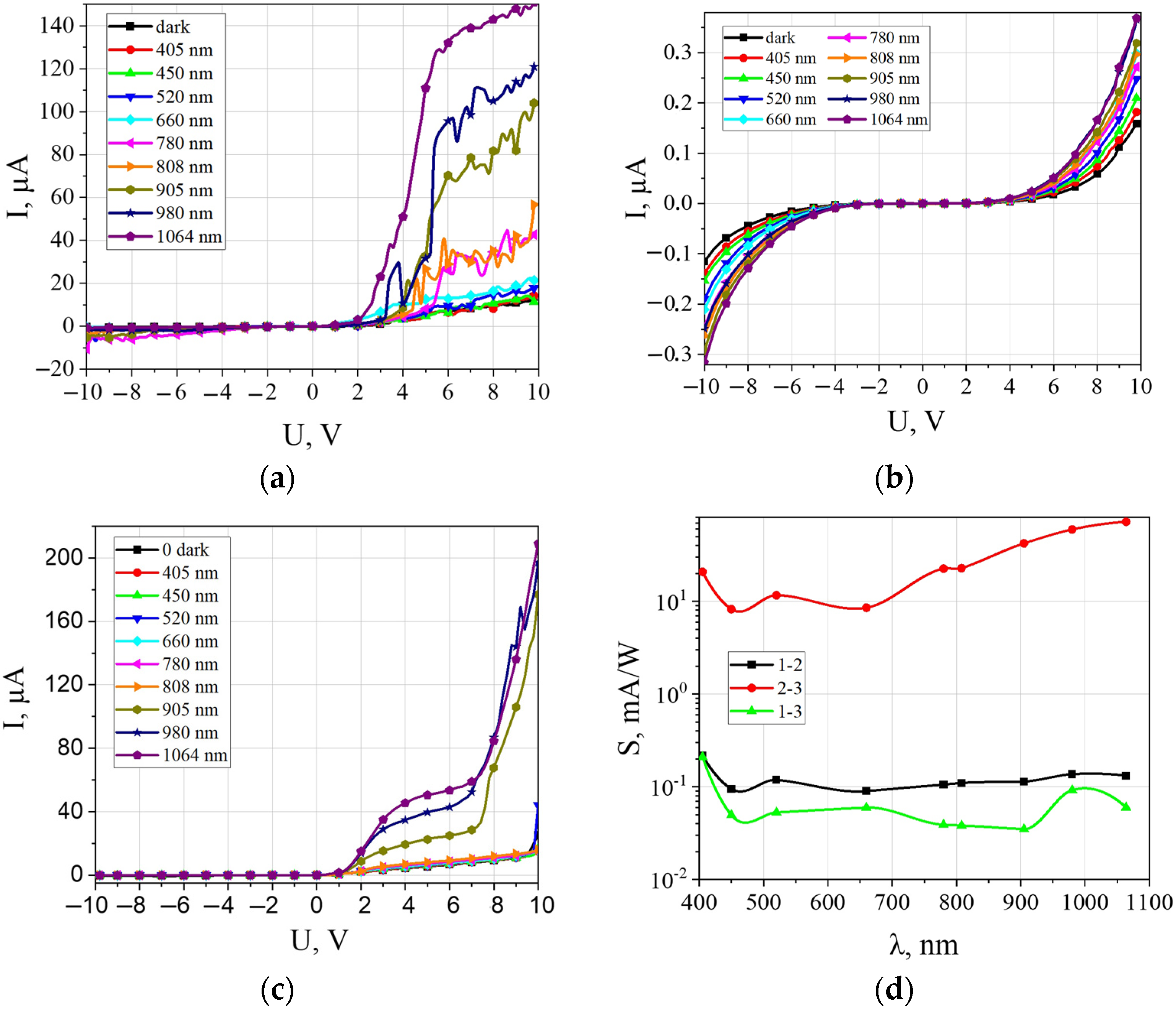
To estimate the photoelectric properties of the structures under investigation, SrTiO
3: xNb/Si/perovskite (x = 0, sample I), and with Nb concentrations of 3 and 6 at.% (samples II and III, respectively), we have measured the I-V characteristics under the influence of radiation with a wavelength from 405 to 1064 nm. An assessment of the spectral sensitivity between different layers was carried out according to the scheme in
Figure 1. The results obtained when measuring between layers of perovskite and silicon (probes 2 and 3,
Figure 1b) are shown in
Figure 4a,
Figure 5a and
Figure 6a; those between layers of perovskite and SrTiO
3 (probes 2 and 1,
Figure 1b) are shown in
Figure 4b,
Figure 5b and
Figure 6b; and those between layers of SrTiO
3 and silicon (probes 1 and 3) are shown in
Figure 4c,
Figure 5c and
Figure 6c. The spectral dependences on the wavelength of the incident radiation at a voltage of +10 V for samples I–III between different layers are shown in
Figure 4d,
Figure 5d and
Figure 6d. Comparison of the measurement results for all three samples will allow us to estimate the contribution of each layer to the photosensitivity of the silicon/SrTiO
3:xNb/perovskite structures.
It can be seen that when measuring the I-V characteristics between layers of perovskite and silicon (
Figure 4a,
Figure 5a and
Figure 6a) for all three samples, the current in the positive voltage region applied to the perovskite layer is larger in absolute value than in the negative voltage region. The observed photoelectric effect is also larger in the region of positive voltages. The conductivity of the structures in the positive voltage region increases with the introduction of Nb by approximately one order of magnitude (see
Figure 5a and
Figure 6a for comparison). However, as the Nb concentration increases from 3 at.% up to 6 at.%, the conductivity is reduced by more than three times. The spectral sensitivity increases from 10–80 mA/W for sample I (without Nb) to values of the order of 10 A/W for sample II (with Nb concentration of 3 at.%), but with increasing Nb concentration to 6 at.% for sample III, it decreases to values of 1–10 mA/W (
Figure 4d,
Figure 5d and
Figure 6d).
I-V characteristics of samples I-III between perovskite and SrTiO
3:xNb layers (
Figure 4b,
Figure 5b and
Figure 6b) are symmetrical, and a visible photoelectric effect is observed at both polarities. The value of the spectral sensitivity is about the same order; however, it slightly exceeds the sensitivity of the order of 0.11–0.12 mA/W in the presence of Nb 3–6 at.% (
Figure 4d,
Figure 5d and
Figure 6d). I-V characteristics of samples between SrTiO
3:xNb and Si layers (
Figure 4c,
Figure 5c and
Figure 6c) have a diode form for all three structures. The visible photoelectric effect is observed in the positive voltage region of I-V characteristics as well as for the entire structure. The spectral sensitivity for sample 1 is 0.03–0.1 mA/V, for sample II it equals 1–5 A/W, and for sample III it equals 1–3 A/W. As in the case of the spectral sensitivity of the entire structure, the maximum value is observed for the SrTiO
3:xNb/Si layer with a Nb concentration of 3 at.%. Thus, we can conclude that the main contribution to the photoconductivity of SrTiO3:xNb/Si/perovskite is carried out by the presence of the SrTiO
3:Nb (3 at.%) transport layer on Si.
As it is well known, SrTiO
3 has its own electronic conductivity due to the appearance of oxygen vacancies there. The properties of SrTiO
3 itself can be easily modified by a slight change in composition. A small addition of Nb makes the material highly conductive (n-type) with a high charge carrier concentration [
21,
22,
25]. This effect manifests itself in an increase in photoconductivity for sample II (
Figure 5). A further decrease in the conductivity of the layers with an increase in the concentration of niobium for sample 3 (
Figure 6) is associated with the distortion of the crystal lattice and an increase in the number of defects that scatter the free electrons.
The observed increase of the photosensitivity in the infrared region of the spectrum (
Figure 4d,
Figure 5d and
Figure 6d) in the form of a maximum at a wavelength of 980 nm is typical for the Si/SrTiO
3 structure (curves 1–3), and with increasing Nb concentration, the maximum decreases. This effect is also traced for the SrTiO
3/perovskite structures (curves 1–2) and Si/SrTiO
3/perovskite (curves 2–3). The sensitivity to IR radiation may be due to the presence of oxygen vacancies, whose density in this material is high [
26].
It should be noted that the measurements of the photoactive properties of the fabricated structures were carried out within a month after their synthesis. During this time, the photoactive properties remained stable.
One of the main factors that significantly affect the properties of SrTiO
3 is the stoichiometric composition as well as the presence of impurities in the crystal structure. The presented experimental data show that Nb doping leads to a change in the photoelectric properties of strontium titanate, which may be due to a change in its dielectric properties during doping [
27]. The substitution of impurity atoms is more likely and energetically favorable as a substitution defect at phase boundaries, interfaces, or surfaces, as a result of which polarized centers can be formed, which are trap centers with weakly bound electrons. It is possible that the introduction of Nb with a concentration of 3 at.% leads to the formation of additional traps involved in the process of photoconductivity, due to which the drift of minority charge carriers in the bulk of SrTiO
3 increases and, accordingly, photoconductivity increases. A further increase in the Nb concentration leads to an increase in the number of traps, as a result of which the probability of recombination mechanisms increases, which can lead to a sharp decrease in the photocurrent. The change in the properties of these films upon doping should be studied in the context of further investigation.

 ,
, 
