Abstract
A dry-etched pedestal chalcogenide waveguide platform, designed for use in long-wave IR spectrometer applications, is demonstrated, fabricated and optically characterized. The optical layers were deposited on pre-patterned dry-etched silicon pedestals. An exceptionally low waveguide propagation loss was measured, at around 0.1 dB/cm at λ = 10 μm. The modal thermo-optic coefficient of the waveguide was experimentally estimated to be approximately 1.1 × 10⁻⁴ C−1 at λ = 1.63 μm, which is comparable to that of Si and GaAs. Waveguide spiral interferometers were fabricated, proving the potential for realization of more complex, chalcogenide-based, integrated photonic circuits. The combination of low propagation losses and a strong thermo-optic coefficient makes this platform an ideal candidate for utilization in on-chip tunable spectrometers in the long-wave IR wavelength band.
1. Introduction
Mid-infrared (mid-IR) on-chip spectrometers have been the cynosure of integrated photonics research for the past few decades, with important advances reported in the literature. The most notable examples of such devices are based on silicon-on-insulator (SOI) [1,2,3], LiNbO3 [4,5] and Ge/Si [6,7] platforms.
Spectrometers operating in the mid-IR spectral region, and more specifically in the long-wave IR region (LWIR-λ = 8–14 μm), are attracting huge interest as their use is essential in many applications such as biomedical and environmental sensing [8]. By using long-wave IR light, it is possible to utilize the unique and wavelength-specific vibration states of molecules, namely the fingerprint absorptions. By analyzing these absorptions, one can extract extremely useful information about a specimen. In addition to long-wave IR being implemented in sensing-related applications, it also finds use in military and non-linear photonic applications [9,10].
The main design challenges of mid-IR on-chip spectrometers are usually related to the limitations introduced by the inherent physical properties of the materials used for the waveguide platform. Most importantly, the materials involved should be transparent in the fingerprint region. As mentioned above, the most commonly used waveguide platforms are based on SOI, LiNbO3 and Ge/Si. Other platforms such as Si3N4 [11] have been used for on-chip spectroscopy; however, they all seem to suffer from inherent absorptions, limiting their use to mostly mid-wave IR wavelengths.
Several types of on-chip spectrometers can be found in the literature such as Fourier transform (FT) [1], digital FT [12] and spatial heterodyne [3,7]. The operation of such devices relies on some form of optical tuning. One of the most common spectrometer configurations is based on the use of an electrically tunable interferometer [1,4]. By applying an external electrical stimulus across one arm of the interferometer, one can tune the effective index (neff) of the propagating mode such that a phase difference is introduced between the light waves travelling through interferometer arms. The resulting interference created when the two beams recombine can be used for the extraction of the spectrum [4].
Depending on the material platform, there are two main effects that are utilized, namely the electro-optic [4,5] and the thermo-optic effect [1,7]. In such spectrometer designs, it is essential that the waveguide platform used is not only transparent but also has a low optical loss and is efficiently tunable in the spectral region of interest.
In previous work [13], we have demonstrated the use of a novel chalcogenide combination of optical layers consisting of a GeAsSeTe (IG3) core and GeAsSe (IG2) claddings for the realization of a waveguide platform that can guide light of wavelengths up to at least 11.5 μm with low propagation losses. When working with chalcogenide layers, it is vital to avoid as much post-deposition processing as possible, as it is known that such layers are prone to chemically induced degradation. Common etchants, as well as the developers used during photolithography, are examples of chemicals that can cause significant damage to the deposited chalcogenide layers [14]. To avoid this, Si micromachining was used, through which Si pedestals were realized and used as the base for the subsequent optical layer deposition. The wet-etching-based fabrication method used in [13] is repeatable and cost-effective but can only produce straight waveguides. Thus, it poses a limit on applications, as it cannot be used to produce non-straight waveguide geometries. This is due to the nature of the silicon crystal planes, which inherently etch faster or slower depending on their direction.
This paper explores the optical properties of a dry-etched pedestal chalcogenide waveguide platform which utilizes the same layer structure as in our previous work [13]. The methods used to fabricate the platform presented here can effectively produce waveguides of any geometry as opposed to the wet etch method that was presented before [13]. This, along with the good refractive index tunability, proves that this platform is a potential candidate for use in tunable spectroscopy applications. The propagation loss and the modal thermo-optic coefficient (TOC) of the platform are presented here, along with details on fabrication and characterization methods.
2. Waveguide Fabrication
As previously discussed, the main process for the fabrication of the waveguides is based on the patterning of Si wafers to produce pedestals using common microfabrication methods. For this dry etching approach, Si (100) wafers with a thermally grown oxide layer were used. The oxide layer was used as a hard mask during the Si etching process. Similar to the process followed in [13], S1813-based photolithography was utilized. Etching of both the oxide mask and silicon was performed on a deep reactive ion etching (PlasmaTherm Versaline ICP) system. The oxide mask was patterned using C4F8 gas and the exposed Si was etched using a standard Bosch process based on a SF6/C4F8 gas cycle. The optical layers were thermally evaporated on top of the Si pedestal in a similar manner to that described in [13].
Figure 1 shows optical microscope images of (a) a cross section of a waveguide and (b) the top surface of a spiral Mach Zehnder interferometer (MZI). It is evident from the cleaved facet of the waveguide in (a) that the optical layers are of high quality, as there are no signs of a large grain structure or cracks. An interesting observation in Figure 1a is the deposition masking effect, seen as a reduced material deposition on either side of the waveguide. This inherent property of the platform can help reduce the required Si etch depth, since the layers deposited in the etched trenches do not come into contact with either the pedestal or more importantly, the waveguide. A reduction in the required etch depth makes the process much more efficient. The picture of the spiral MZI presented in Figure 1b confirms the capability of the process to realize more complex waveguide structures with high-quality surfaces and without discontinuities.
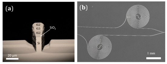
Figure 1.
Pedestal waveguides fabricated using the Bosch etch process. (a) Cross-section and (b) spiral MZI.
3. Optical Loss
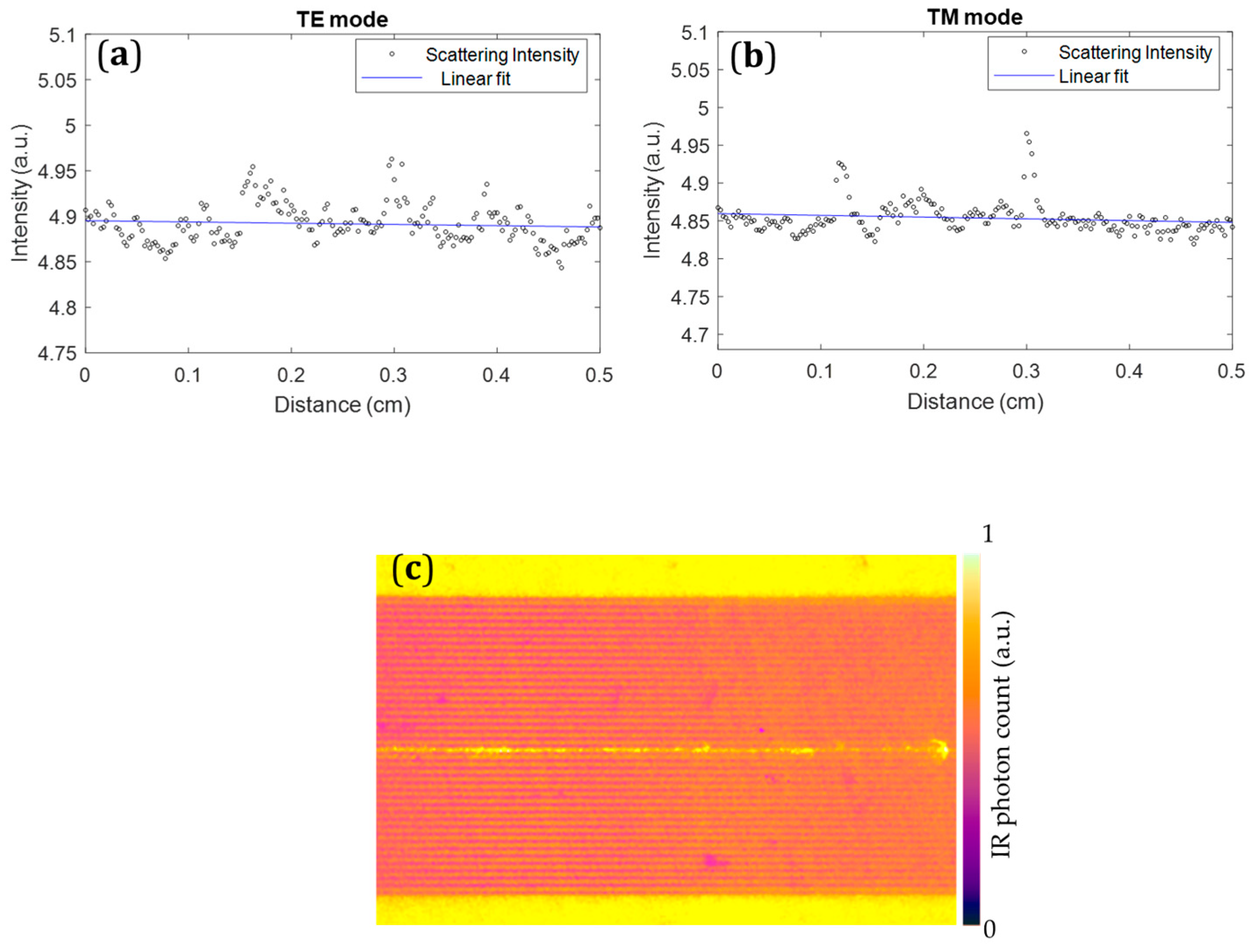
The waveguiding and propagation loss estimation of the waveguides was performed using a mid-IR quantum cascade laser (QCL). The light from the laser was end-fire coupled to the cleaved facet of the waveguide using a ZnSe objective lens. The scattered light from the top surface, as well as the light scattering at the input and output facets of the waveguide, was viewed using an infrared camera. The propagation loss was estimated by fitting the scattered light streak collected by the infrared camera, as also described in [13]. Figure 2c shows the streak of the scattered light that emanates from the top surface of the waveguide. This waveguide was used for the estimation of the propagation loss. Its layer structure is shown in Figure 1a. The linear fit of the decaying scattered light is presented in Figure 2a,b. Using the linear fit slope of the decaying scattering data, the propagation loss is estimated to be 0.08 ± 0.02 dB/cm and 0.1 ± 0.02 dB/cm for TE and TM modes at λ = 10 μm, respectively. Measurements on similar waveguides fabricated using the same process provided very similar loss figures of 0.2 ± 0.1 dB. The slightly higher loss for TM polarization could either bea result of higher radiation of the mode into the Si substrate due to the nature of the TM mode E-field distribution or a variation from error in the data.

Figure 2.
Scattering intensity vs. distance. The slope of the linear fit was used for the estimation of the propagation loss of the (a) TE mode and (b) TM mode. (c) Streak of light along the waveguide surface.
The propagation losses of these chalcogenide waveguides are amongst the lowest reported [15] in the long-wave IR to the best of the knowledge of the authors. A large part of the loss in these waveguides originates from light scattering off large, discrete scattering centers which are distributed along the length of the waveguides. These defects most likely originated from material splashing during deposition as a result of the different material vapor pressures present in the quaternary alloy. Although a baffled deposition source box was used in order to prevent such effects, fluctuations in the deposition rate suggested that it remained an issue. A better and more stable layer deposition could potentially reduce the density of such defects and make these waveguides present an even lower loss, which is ideal in applications that utilize long waveguides. This could potentially be achieved by using another thermal evaporator or by optimizing the process even more extensively.
4. Thermo-Optic Measurements
In order to estimate the thermo-optic coefficient of the waveguides, a simple apparatus which consisted of a tunable laser source, a heated stage and a detector was used. The measurements were performed at λ = 1620–1640 nm instead of the mid-IR region due to the availability of a high-resolution distributed feedback laser in that wavelength range. The light was coupled in and out of the waveguide using silica fibers which were butt-coupled to the facets of the waveguide. To heat the sample, a Peltier module was used. The sample itself was placed on an aluminum block, which was placed on the Peltier module, as seen in Figure 3. A hole was drilled in the middle of the aluminum block, into which the thermocouple was placed. The Peltier module was powered by a benchtop DC power supply. The waveguide chips were always shorter than the width of the aluminum so that the whole waveguide length would be heated up adequately to reduce the possibility of underestimation of the TOC. To ensure that the waveguide chip reached the target temperature, which was normally monitored in the middle of the aluminum block, each data acquisition was performed after around one minute from each temperature change, to allow the temperature at the waveguide level to come to a steady state. The tests that were performed prior to measurements in which the temperature in the middle of the aluminum block and at the top of the waveguide chip was monitored using two different probes, showed that it only takes a few seconds to reach a steady state.
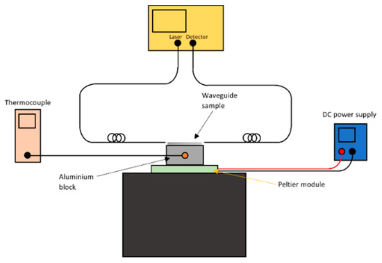
Figure 3.
Diagram of the apparatus used for the measurement of the waveguide’s effective TOC.
There is a plethora of different methods that can be used to estimate the TOC, with the most common ones relying on the use of a resonant optical cavity [16,17]. In order to estimate the TOC using an optical cavity, one can detect the change in the refractive index of a material, or in the case of a waveguide, a change in the ng, by tracking the resonance wavelength shifts as a function of a change in temperature.
The measurements for the estimation of the IG2/IG3 waveguide modal TOC, which is the thermal dependance of the effective index of the waveguide, were performed on a straight waveguide with cleaved facets. The quality of the cleave was good enough to provide clear Fabry–Perot (FP) resonances. Although only the effective TOC can be extracted through these measurements since it represents the change in the modal refractive index, it is an accurate representation of expected thermo-optic tunability of these waveguides. Estimating the TOC for each layer individually is not possible in this case as it would require knowing the TOC of at least one of the layers. The TOC coefficient can be estimated using the FP data and the equations listed below.
where L is the round-trip length, ng is the estimated group index and ∂λ/∂Τ is the temperature-induced shift in the FP resonances.
The waveguide used for the thermo-optic measurements was fabricated in a similar manner to those described earlier; however, since the waveguides for TOC estimation are measured in the near-IR, the etch depth and thicknesses of the optical layers were adjusted accordingly.
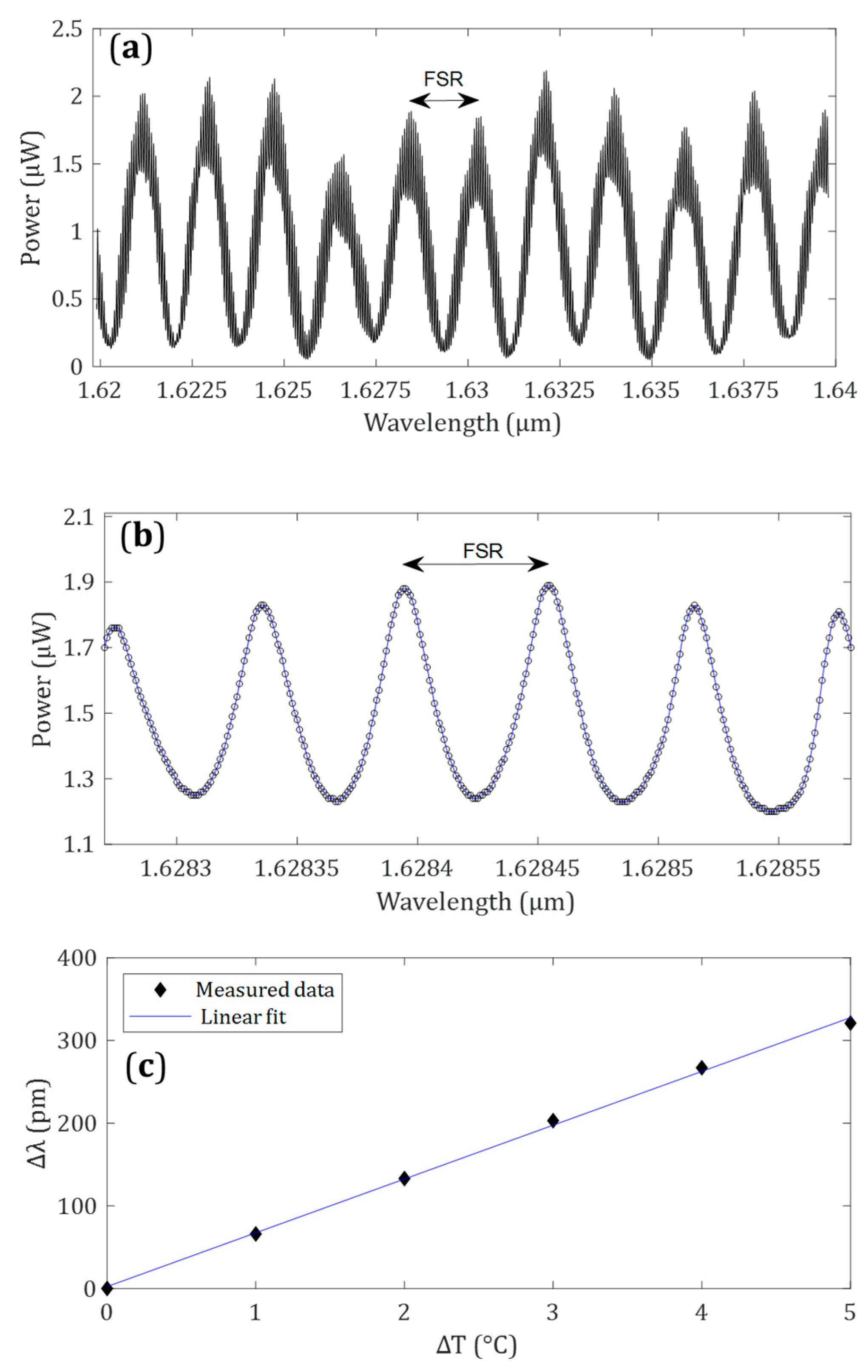
The total effective waveguide length was approximately 0.79 cm; thus, the round trip/cavity length was ~1.58 cm. The spectrum retrieved from the waveguide is given in Figure 4a. It is evident that a very strong type of interference is present in the measurement with an approximate period of 1.8 nm. The neff and ng of the fundamental TE waveguide mode were numerically estimated to be around 2.762 and 2.926 at λ = 1630 nm, respectively. Using this ng value in Equation (1), a much smaller FSR of around 57.5 pm is obtained for a waveguide length of around 0.79 cm. It was thus concluded that this interference was not an effect of the FP cavity and most likely originated from mode beating.

Figure 4.
A 1 pm resolution wavelength scan taken at room temperature. (a) Full spectral scan between 1.62 and 1.64 μm wavelength—the FSR is approximately 1.8 nm. (b) Zoomed-in version of (a) for better FP signal viewing. (c) Linear fit of Δλ measured data.
A zoomed-in version of the measured signal, showing these resonances, is given in Figure 4b. The obtained FSR was 60 pm, which was very similar to the value obtained using the numerically estimated group index (i.e., 57.5 pm). This confirmed that these Lorentzian-shaped resonances indeed originated from the FP cavity formed between the waveguide end facets. The slight difference between the measured and numerically estimated FSR values was most likely due to differences between the waveguide-modelled and real geometry.
In order to estimate the wavelength shift of the FP resonances with increasing temperature, the measurement data taken at 1 °C increments were filtered using fast Fourier transform (FFT) bandpass filters to remove all the signal components except for the FP-related resonances. By doing this, it was possible to estimate the effective TOC of the waveguide platform. The resonance shift against temperature is given in Figure 4c. The derivative of the resonance shift and temperature was found to be 65.1 pm/°C. Using Equation (2), the TOC was estimated to be ~1.1 × 10⁻⁴ °C−1. Based on the IG2/IG3 material specifications, and the fact that the measurements presented in this work were performed far from the band edge of the material system, it is expected that the TOC will not present strong dispersion and thus maintain its amplitude even in the LWIR range. Compared to other commonly used thermo-optic waveguides such as Si and GaAs [18], which both have a TOC of around 2 × 10⁻⁴, the IG2/IG3 platform shows a comparable TOC value, making it a strong candidate for use in on-chip tunable spectrometers.
5. Conclusions
A simple Bosch etching process was followed for the fabrication of complex IG3/IG2 pedestal waveguides. These waveguides were designed for use in a tunable interferometer which will be utilized as an on-chip spectrometer in the LWIR. The proof-of-principle spectrometer design contains long, tunable waveguide spirals. It was thus essential that the waveguide platform had low propagation losses as well as strong tunability. The propagation loss estimation yielded one of the lowest reported loss figures for chalcogenide waveguides in the mid-IR of less than 0.1 dB/cm at λ = 10 μm. In addition, the thermo-optic experiments conducted on straight pedestal waveguide cavities showed strong FP resonances, which shifted greatly with temperature increases. The estimated modal TOC was ~1.1 × 10⁻⁴ °C−1 at λ = 1.63 μm. This value is comparable to that of Si and GaAs, which are two of the most used waveguide materials in thermo-optic applications. The ease of fabrication, low propagation losses and relatively strong TOC compared to other thermo-optic waveguide platforms, prove that such a platform can be ultimately used in many applications in the LWIR region and particularly in mid-IR tunable spectroscopy.
Author Contributions
G.S.M. conceived the idea. V.M. developed and performed the fabrication, characterization and analysis of the chips with input from S.B. The paper was written by V.M. with input from J.S.W. and G.S.M. All authors have read and agreed to the published version of the manuscript.
Funding
This work was supported by the Royal Society International Exchanges Grant IEC\NSFC\201068 and “The Future Photonic Hub” (UK EPSRC grant EP/N00762X/1).
Institutional Review Board Statement
Not applicable.
Data Availability Statement
The data for this work are accessible through the University of Southampton Institutional Research Repository “https://eprints.soton.ac.uk/ (accessed on 23 February 2024)”.
Conflicts of Interest
The authors declare no conflicts of interest.
References
- Souza, M.; Grieco, A.; Frateschi, N.C.; Fainman, Y. Fourier transform spectrometer on silicon with thermo-optic non-linearity and dispersion correction. Nat. Commun. 2018, 9, 665. [Google Scholar] [CrossRef] [PubMed]
- Nedeljkovic, M.; Stankovic, S.; Mitchell, C.J.; Khokhar, A.Z.; Reynolds, S.A.; Thomson, D.J.; Gardes, F.Y.; Littlejohns, C.G.; Reed, G.T.; Mashanovich, G.Z. Mid-Infrared Thermo-Optic Modulators in SoI. IEEE Photonics Technol. Lett. 2014, 26, 1352–1355. [Google Scholar] [CrossRef]
- Nedeljkovic, M.; Velasco, A.V.; Khokhar, A.Z.; Delage, A.; Cheben, P.; Mashanovich, G.Z. Mid-Infrared Silicon-on-Insulator Fourier-Transform Spectrometer Chip. IEEE Photonics Technol. Lett. 2016, 28, 528–531. [Google Scholar] [CrossRef]
- Bentini, G.G.; Bianconi, M.; Cerutti, A.; Chiarini, M.; Pennestrì, G.; Sada, C.; Argiolas, N.; Bazzan, M.; Mazzoldi, P. Integrated Mach-Zehnder micro-interferometer on LiNbO3. Opt. Lasers Eng. 2007, 45, 368–372. [Google Scholar] [CrossRef]
- Li, J.; Lu, D.F.; Qi, Z.M. Miniature Fourier transform spectrometer based on wavelength dependence of half-wave voltage of a LiNbO3 waveguide interferometer. Opt. Lett. 2014, 39, 3923–3926. [Google Scholar] [CrossRef] [PubMed]
- Liu, Q.; Ramirez, J.M.; Vakarin, V.; Le Roux, X.; Alonso-Ramos, C.; Frigerio, J.; Ballabio, A.; Simola, E.T.; Bouville, D.; Vivien, L.; et al. Integrated broadband dual-polarization Ge-rich SiGe mid-infrared Fourier-transform spectrometer. Opt. Lett. 2018, 43, 5021–5024. [Google Scholar] [CrossRef] [PubMed]
- Montesinos-Ballester, M.; Liu, Q.; Vakarin, V.; Ramirez, J.M.; Alonso-Ramos, C.; Roux, X.L.; Frigerio, J.; Ballabio, A.; Talamas, E.; Vivien, L.; et al. On-chip Fourier-transform spectrometer based on spatial heterodyning tuned by thermo-optic effect. Sci. Rep. 2019, 9, 14633. [Google Scholar] [CrossRef] [PubMed]
- Haas, J.; Mizaikoff, B. Advances in Mid-Infrared Spectroscopy for Chemical Analysis. Annu. Rev. Anal. Chem. 2016, 9, 45–68. [Google Scholar] [CrossRef] [PubMed]
- Soref, R.A.; Emelett, S.J.; Buchwald, W.R. Silicon waveguided components for the long-wave infrared region. J. Opt. A Pure Appl. Opt. 2006, 8, 840. [Google Scholar] [CrossRef]
- Dingding, R.; Dong, C.; Burghoff, D. Integrated nonlinear photonics in the longwave-infrared: A roadmap. MRS Commun. 2023, 13, 942–956. [Google Scholar]
- Subramanian, A.Z.; Ryckeboer, E.; Dhakal, A.; Peyskens, F.; Malik, A.; Kuyken, B.; Zhao, H.; Pathak, S.; Ruocco, A.; De Groote, A.; et al. Silicon and silicon nitride photonic circuits for spectroscopic sensing on-a chip. Photonics Res. 2015, 3, B47–B59. [Google Scholar] [CrossRef]
- Kita, D.; Miranda, B.; Ríos, C.; Favela, D.; Bono, D.C.; Michon, J.; Lin, H.; Gu, T.; Hu, J.; Crocombe, R.A.; et al. Chip-scale high-performance digital Fourier Transform (dFT) spectrometers. In Next-Generation Spectroscopic Technologies XII; SPIE: Baltimore, MD, USA, 2019. [Google Scholar]
- Mourgelas, V.; Sessions, N.P.; Wilkinson, J.S.; Murugan, G.S. Etchless pedestal chalcogenide waveguide platform for long-wave IR applications. Opt. Mater. Express 2022, 12, 1154–1162. [Google Scholar] [CrossRef]
- Yan, T.-Y.; Shen, X.; Wang, R.-P.; Wang, G.-X.; Dai, S.-X.; Xu, T.-F.; Nie, Q.-H. Hot-embossing fabrication of chalcogenide glasses rib waveguide for mid-infrared molecular sensing. Chin. Phys. B 2017, 26, 024213. [Google Scholar] [CrossRef]
- Gai, X.; Han, T.; Prasad, A.; Madden, S.; Choi, D.-Y.; Wang, R.; Bulla, D.; Luther-Davies, B. Progress in optical waveguides fabricated from chalcogenide glasses. Opt. Express 2010, 18, 26635–26646. [Google Scholar] [CrossRef] [PubMed]
- Pruiti, N.G.; Klitis, C.; Gough, C.; May, S.; Sorel, M. Thermo-optic coefficient of PECVD silicon-rich silicon nitride. Opt. Lett. 2020, 45, 6242–6245. [Google Scholar] [CrossRef] [PubMed]
- Sokolov, S.; Lian, J.; Combrie, S.; De Rossi, A.; Mosk, A.P. Measurement of the linear thermo-optical coefficient of Ga0.51In0.49P using photonic crystal nanocavities. Appl. Opt. 2017, 56, 3219–3222. [Google Scholar] [PubMed]
- Weber, M.J. Handbook of Optical Materials; CRC Press LLC: Boca Raton, FL, USA, 2003. [Google Scholar]


Disclaimer/Publisher’s Note: The statements, opinions and data contained in all publications are solely those of the individual author(s) and contributor(s) and not of MDPI and/or the editor(s). MDPI and/or the editor(s) disclaim responsibility for any injury to people or property resulting from any ideas, methods, instructions or products referred to in the content. |
© 2024 by the authors. Licensee MDPI, Basel, Switzerland. This article is an open access article distributed under the terms and conditions of the Creative Commons Attribution (CC BY) license (https://creativecommons.org/licenses/by/4.0/).