1. Introduction
Surface plasmon polaritons (SPPs) are surface electromagnetic wave (SEW) solutions of the macroscopic Maxwell equations which arise at sharp interfaces between good metals and dielectrics [
1,
2,
3,
4]. SPPs are known to facilitate light transmission through arrays of nanoholes made in thin metal films—see [
5,
6,
7,
8] and references therein. The physical mechanism of this effect is believed to involve the coupling of external light to SPPs propagating on the opposite metal–dielectric interfaces of a metal film.
Very recently, it was demonstrated that another kind of SEW may exist at a gradual interface between two different electromagnetic media [
9]. If a gradual transition region
e(
z) is assumed to exist (as shown in
Figure 1a) at the boundary separating the media (instead of a step-like sharp interface in the
z direction perpendicular to the interface) the wave equation for the TM-polarized surface electromagnetic mode becomes
which coincides with a one-dimensional Schrödinger equation in which the wave function is introduced as
y = e1/2Ez, and
Ez is the electric field component perpendicular to the interface. The effective potential energy
V(
z) in Equation (1) depends on the gradient terms, and the effective total energy −
k2 is defined by the SEW wave vector
k along the interface. As demonstrated in [
9], the gradient terms may become the dominating terms in Equation (1), leading to the appearance of unconventional propagating SEW solutions, even in the case of a gradual boundary between two strongly lossy materials in which
e(
z) is large and almost pure imaginary.
While the strongly lossy case may be very interesting in such diverse applications as UV nanophotonics and underwater communications [
9], in this article, we consider a different situation of a gradual interface between two different good low-loss metals, such as gold and silver (see
Figure 1). We demonstrate that a gradual interface between gold and silver supports the propagation of a novel kind of surface electromagnetic wave, which is different from the more well-known surface plasmon polaritons. The existence of such surface waves leads to a paradoxical situation in which a continuous metal barrier which does not have any pinholes may exhibit a considerably increased light transmission if the barrier is made of two different metals.
2. Materials and Methods
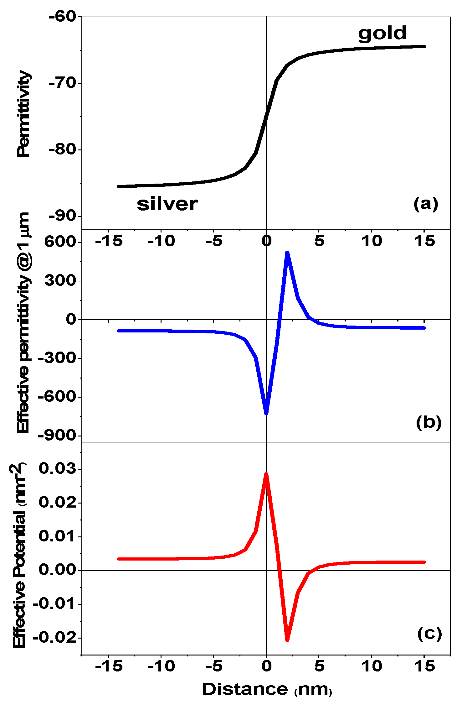
As illustrated in
Figure 1a, in the visible and near infrared ranges
e(
z) of such a system will be large, negative, and almost pure real. As an example, the transition region between gold and silver is assumed to be about 10 nm deep. Such a gradual interdiffusion layer would form naturally if a silver film were formed on top of a gold film via thermal evaporation [
11]. The corresponding effective potential
V(
z) calculated using Equation (1) is shown in
Figure 1c at
λ = 1 mm. While the magnitude of the dielectric permittivity change across the interface may differ depending on the wavelength, its gradual character is determined by the same width of the interdiffusion region. Let us evaluate if a propagating SEW solution may be expected for such a potential well.
The easiest way to demonstrate that such an SEW solution does exist in this case is to introduce an effective permittivity of the transition layer as
thus incorporating the gradient terms from Equation (1) into the “effective” permittivity so that Equation (1) may be rewritten as
The so-obtained effective dielectric permittivity of the transition layer is plotted in
Figure 1b. The latter plot demonstrates that a gradual interface between gold and silver is equivalent to a parallel plate metallic waveguide which is known to have no cutoff frequency for the TM-polarized light and which always supports a TM
0-guided mode (note the region of positive
eeff in between the two negative
eeff regions in
Figure 1b). Indeed, using the Numerov method [
12], Equation (1) may be solved numerically for the geometry depicted in
Figure 1. At the free space wavelength of
λ0 = 1 mm, such a numerical solution results in −
k2 = −0.00345 nm
−2, which leads to
k = 0.059 nm
−1 and
λ = 106 nm for the guided TM-polarized SEW mode. While the SEW propagation length for a perfectly flat interface is defined by Im(
k) [
9], in most practical situations, the propagation length will be defined by surface roughness.
The interfacial geometry shown in
Figure 1 was also simulated numerically with method of moments, as shown in
Figure 2, using the commercial EM solver Altair Feko [
13]. The transition between gold and silver was modeled in Feko as an infinite planar multilayer substrate consisting of ten 1 nm thick layers with the dielectric constant gradually changing from the dielectric constant of gold (
eAu = −75 +
i∙5) to the dielectric constant of silver (
eAg = −85 +
i∙5). Feko’s special Green’s function formulation (method of moments extension) implemented 2D infinite planes with finite thickness to model each layer of the electromagnetic medium. The stack of these layers was sandwiched between semi-infinite layers of gold and silver. These layers were defined in Feko as homogeneous half spaces (exact Sommerfeld integrals). Electromagnetic waves were excited by a point electric dipole with a magnitude of
Idl = 1 A∙m and a frequency 300 THz. The point source was placed in the center of the 10-layer substrate (transition layer). It was directly parallel to the layers and perpendicular to the observation plane in
Figure 2. As seen in these simulations, the SEW propagation length for an ideally planar interface (with no surface roughness) may reach at least ~10 mm—see the top and the middle images in
Figure 2, which show the magnitude of the Poynting vector and the z-component of the electric field in the simulated structure, respectively. These results are consistent with the predictions of the analytical model. In particular, the wavelength of the SEW mode obtained in these simulations (
λ = 106 nm—see the phase image in the bottom of
Figure 2) closely matches the analytical predictions.
Note that the obtained solution cannot be classified as a conventional SPP mode. The wave vector
k of a conventional SPP mode is defined as follows [
1,
9]:
where
ε1 and
ε2 are the dielectric permittivities of the neighboring media. When both
ε1 and
ε2 are mostly real and negative, Equation (4) produces an almost pure imaginary value of the
k vector, indicating the absence of the SPP mode.
3. Results
Our experimental results on light propagation through gold–silver interfaces appear to be consistent with the theoretical predictions and numerical simulations described above. Since the direct probing of the SEW field at the gold–silver interface using scanning probe techniques is not possible, we investigated light transmission through composite gold–silver films fabricated on glass slides using thermal evaporation. These experimental results are summarized in
Figure 3,
Figure 4 and
Figure 5.
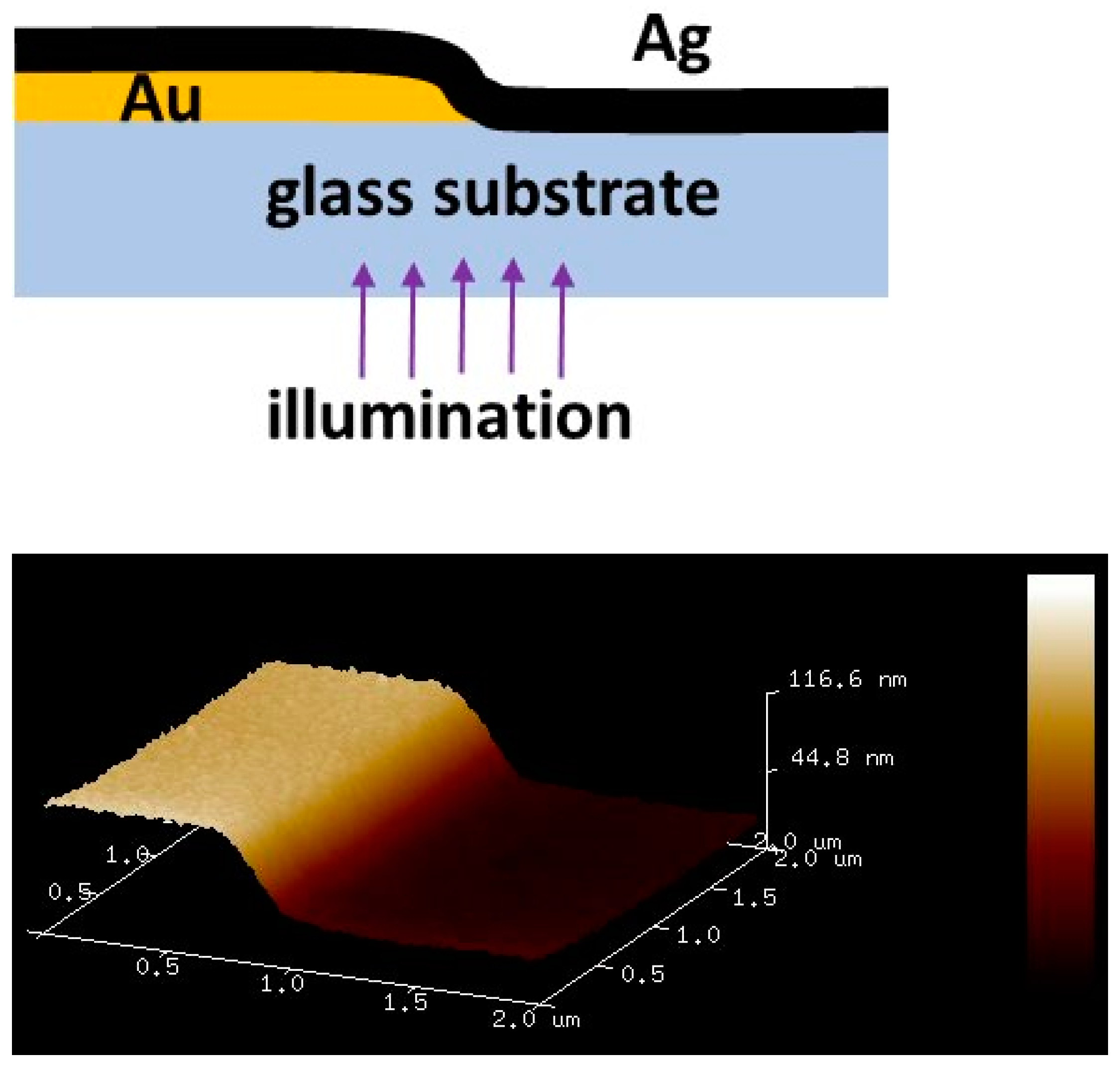
The composite gold–silver films were fabricated on top of glass slides overcoated with a thin (5 nm) chromium layer for adhesion, as illustrated in
Figure 3. Such an extremely thin uniform layer of chromium did not affect the results of our optical transmission experiments. The glass substrates used in this study were Corning boro-aluminosilicate glass slides which exhibited a typical surface roughness of <0.02 micrometer/5 mm peak to peak.
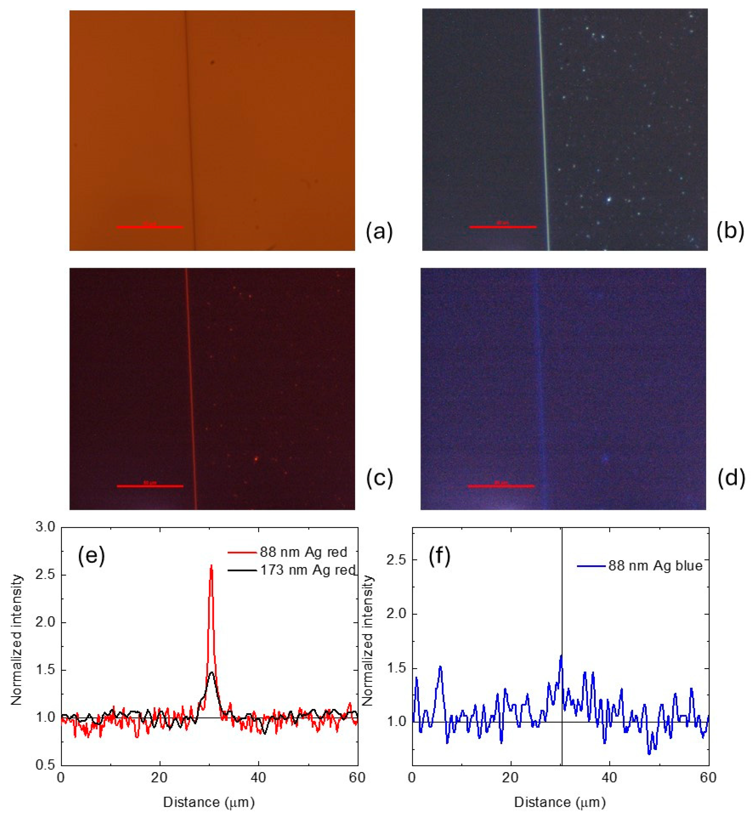
The fabrication method was as follows. A pattern consisting of 2 mm wide stripes of photoresist was made using negative photoresist APOL-LO 3204 on a 0.5 mm thick glass slide. A 5 nm adhesive layer of chromium followed by an 80 nm thick layer of gold were deposited via thermal evaporation, and lift-off was performed. Then, a layer of silver was deposited via thermal evaporation over the pattern of 2 mm wide gold stripes. The sample shown in
Figure 4a consisted of an 80 nm gold film (on the left) overcoated with an overlap with an 88 nm thick silver film. The schematic geometry of this sample is illustrated in
Figure 3. Optical microscope images of the overlap region obtained in reflection (
Figure 4a) and transmission (
Figure 4b–d) using white light illumination are shown in these figures. As clearly seen in
Figure 4b, a stripe of strongly enhanced light transmission is observed near the edge of the gold–silver overlap region, which goes in parallel with the edge.
Figure 4c–f summarize the results of our spectroscopic studies of this effect. It appears that the red light transmission far exceeds the transmission of blue light through the Au/Ag junction. This is clear from both the transmission images obtained with color filters and from the comparison of their cross-sectional plots presented in
Figure 4e,f through the stripe region. Moreover, when the silver film thickness is increased to 173 nm, the transmission of red light through the junction remains quite considerable (see
Figure 4e), while the blue light transmission becomes undetectable at the current sensitivity of our experiments. The observed effect shows very weak or no dependence on the polarization of illuminated light, which is consistent with the theoretically predicted TM character of the gradient SEW. Both the transverse and longitudinal electric field components of the SEW mode are non-zero.
Our experimental results are consistent with the novel theoretical mechanism discussed in
Section 2. Indeed, based on Equation (1), the effective potential
V(
z) at the Au/Ag interface is mostly real at longer wavelengths, where the dielectric permittivities of both gold and silver are large, negative, and mostly real. On the other hand,
V(
z) acquires a considerable imaginary part towards at the blue light wavelengths. Note that these results are drastically different from the naïve expectations based on the known wavelength-dependent skin depth in gold and silver. Note that the skin depth of silver at the red light 600 nm wavelength equals about 14 nm [
14]. This means that based on conventional expectations, light would need to be transmitted through at least 12 skin depths, which makes this effect somewhat similar to previous experimental observations of enhanced SEW transmission underwater [
15].
We verified, using AFM imaging (see the bottom part of
Figure 3), that the integrity of the composite gold–silver film was not compromised in any way near the gold–silver edge (it did not contain any pinholes or crevices near the edge). The AFM image in
Figure 3 is a representative image which covers approximately the area of the observed enhanced light transmission. Multiple other images taken across the larger observation area showed approximately the same surface roughness. Therefore, the effect of enhanced optical transmissions near the gold–silver edge cannot be attributed to defects of the composite film.
We also verified that a similar effect was observed in the infrared range using an SWIR microscope camera—see
Figure 5. The sample used in this experiment was fabricated in a similar fashion. An 80 nm gold film (on the left) was overcoated with an overlap with a 50 nm thick silver film. A similar stripe of strongly enhanced IR transmission was observed in the Au/Ag junction region.
4. Discussion
Based on the obtained theoretical and experimental information, we must conclude that the effect of enhanced light transmissions through the composite gold–silver film may be connected to the existence of novel SEW modes at the gold–silver interface. Similar to SPP-mediated light transmissions through nanohole arrays [
5,
6,
7,
8], these novel SEW modes may facilitate the transmission of light through a continuous composite metal film. Indeed, according to Fermi’s golden rule [
16], the increased transmission of light at the gold–silver junction indicates an increased density of photonic states (DOS) in the general area of the junction, which becomes available to the photons tunneling through the composite metal film. This increase may occur due to the surface topography step (see
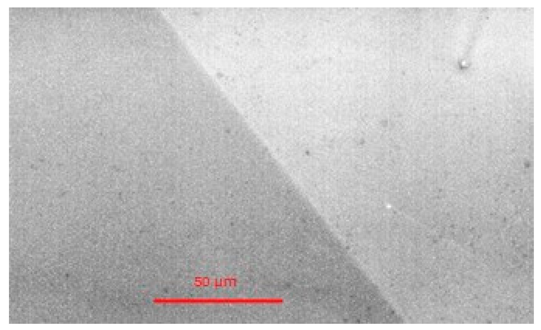
Figure 3) which breaks the momentum conservation law and facilitates the coupling between photons and surface plasmons of the metal films. However, this mechanism is excluded by our control experiments with Ag/Ag junctions in which a silver film of similar thickness was overcoated with another silver film, and no enhanced transmission was observed (see
Figure 6—compare with
Figure 4a,c). The newly discovered interfacial states of the gold–silver interface are another source of the DOS increase, which becomes available to the tunneling photons. Therefore, a strong increase in light transmissions near the Au/Ag junction (in the demonstrated absence of the topographical effects) is a strong indication in favor of our theoretical model.
We should also mention that based on Equations (1) and (2), somewhat similar SEW modes must also exist at gradual interfaces between two dielectrics. Indeed, in such a case, the shapes of the effective potential and the effective permittivity curves from
Figure 1b,c, which are mostly affected by the gradient terms, will look similar to the case of a gradual interface between two metals, which was considered above. Therefore, a TM-polarized SEW solution must also exist in the dielectric case, which has a
k vector larger than the
k vector of photons in each neighboring medium. The existence of such surface waves may have affected observations in ref. [
17], which reported considerably enhanced light transmission through opaque samples, even in the absence of surface plasmon polariton modes. In addition, the existence of such large
k vector SEW modes in the dielectric samples may lead to interesting new possibilities of performing super-resolution microscopy experiments using purely dielectric low-loss materials. This may be accomplished by either implementing some of the SEW-based 2D microscopy geometries [
18,
19] or by appropriately modifying recent experiments with high-index liquid-immersed microspheres [
20].
As noted in ref. [
9], the new kind of “gradient” surface electromagnetic waves, which are experimentally observed in this work, may exist in experimental domains (such as UV nanophotonic devices) which are currently not accessible to more conventional plasmonic nanophotonic devices. Thus, our work further extends the boundaries of the fast-moving field of novel optical materials which has experienced numerous exciting recent advances [
21,
22,
23,
24,
25,
26]. In particular, optical losses appear to be one of the main obstacles for the broader implementation of photonic crystal, plasmonic and optical metamaterial devices—see refs. [
23,
24,
25,
26]. Theoretical prediction that “gradient” surface waves exist even in high-loss situations opens up a broad range of new materials available for metamaterial design. For example, silicon nanophotonic devices may become a near-future reality [
9]. As noted above, experimental confirmation of “gradient” surface electromagnetic waves may also open up new spectral ranges where such new optical materials and devices may be realized, such as deep UV nanophotonics, where high optical losses are unavoidable. Therefore, new experimental observations reported in our paper appear to be quite consequential.


