Abstract
The emergences of silicon-based photonic crystal (PhC) waveguides and two-dimensional (2D) PhC line-defect optical cavities have revolutionized the field of integrated photonics. In this paper, we design and fabricate a high-quality (high-Q) 2D silicon-based PhC optical cavity with integrated waveguides. We employ the 2D finite-difference time-domain (FDTD) method to simulate the cavity, considering two different thicknesses: 0.5 μm and 0.25 μm. By optimizing the line-defect and air-slot widths for the integrated PhC waveguides, we are able to achieve remarkable Q-factors for the PhC optical cavity. With a silicon thickness of 0.5 μm, the high-Q achieves an impressively high value of 8.01 × 10⁶, while at a silicon thickness of 0.25 μm, it achieves 1.91 × 10⁷. This research highlights the importance of design optimization and fabrication techniques in achieving high-Q optical devices using PhC and silicon-based structures.
1. Introduction
Optical cavities, also known as optical resonators, are crucial components in photonics, enabling precise control and manipulation of light for various scientific and technological applications [1,2,3,4,5,6]. These cavities trap light within resonant structures, resulting in enhanced optical effects and a wide range of functionalities [7,8]. A commonly used type involves the Fabry–Perot cavity [9] and whispering-gallery mode (WGM) cavities [10], like microdesk cavities [11], microsphere cavities [12], and microtoroid cavities [13]. Ring resonators have various uses in the field of integrated photonics [14], including optical filters [15], modulators [16], and delay lines [17]. Photonic crystal (PhC) cavities utilize periodic dielectric patterns to confine light and generate band gaps designed for specific wavelengths. They possess impressive qualities and exhibit powerful interactions between light and matter, which make them highly desirable in various fields, such as integrated photonics [14], optical sensors [18], and on-chip quantum information processing [19,20]. Silicon-based PhC optical cavities present a number of challenges that researchers are actively working to overcome. The main areas of focus include achieving high fabrication precision, optimizing light coupling efficiency, minimizing losses, and seamlessly integrating with active components [21]. In [22], a novel compact demultiplexing structure is proposed, utilizing enhanced shell-type ring resonators within a PhC architecture for dense wavelength-division multiplexing (DWDM) systems, with near-perfect transmission efficiency and a high-Q of 15,497. However, integrating lower refractive index spheres as mirrors may introduce fabrication complexities and pose implementation challenges.
In recent years, integrating silicon-based PhC waveguides with silicon PhCs has become a crucial technology for various applications, including optical communication [23], sensing [24], nonlinear optics [25], and quantum photonics [26]. In [27], the authors introduced a PhC slab cavity with width modulation of the line defect, achieving an ultrahigh Q-value of 7 × 10⁷ through the simple displacement of two holes from the line defect. However, it should be acknowledged that this approach heavily relies on the displacement of two holes from the line defect. A new method for calculating the high-Q of a 2D PhC nanocavity directly from a 2D mode profile at the center of a PhC slab was demonstrated in [28].
Additionally, the combination of silicon-based PhC cavities and silicon-based PhC waveguides plays a crucial role in integrated photonics. These integrated components bring forth a multitude of benefits, such as their compact size, impressive, high-Q and excellent light confinement properties [29,30,31]. PhC waveguides that exploit slow light and self-collimation significantly enhance the performance of integrated photonic devices. By reducing group velocity, these waveguides improve light–matter interactions and extend effective interaction lengths [32,33]. Combined with high-Q PhC cavities, they enhance light confinement and coupling efficiency, thereby optimizing device functionality [34]. In [35], the authors proposed a novel structure of photonic cavities by introducing arbitrary point defects in 2D PhCs. While this approach offered flexibility in designing cavity structures, it faced challenges in controlling and positioning the point defects precisely. In [36], a systematic numerical investigation of a cavity optomechanical structure based on a lithium niobate PhC cavity was conducted. This study involves designing 2D PhC slabs made of lithium niobate and analyzing their optical properties. This paper also examines the influence of nanofabrication errors. In [37], the authors introduced a PhC waveguide on thin-film lithium niobate, which offers precise light control and is ideal for miniaturized optical devices. They explored mode characteristics and the impact of duty cycles, achieving single-mode transmission and mode conversion. In this paper, we conduct the comprehensive design and simulation of a high-Q 2D silicon-based PhC optical cavity with an integrated PhC waveguide and silicon waveguide and also perform fabrication experiments followed by measurements. We aim to provide a detailed analysis of the performance of the integrated PhC optical cavity to validate our findings through experimental measurements.
2. Investigation of Silicon-Based PhC Waveguide
- A.
- Band gap investigation for the 2D PhC slab
Photonic band gap (PBG) waveguides are advanced structures formed by introducing a defect in a PhC, which has a periodic variation in the refractive index, creating a band gap where light cannot propagate [38]. By disrupting this periodicity, specific wavelengths are guided through the defect path. This mechanism relies on the Bragg effect, where waves are reflected in periodic structures, forming band gaps through constructive interference [39]. This controlled light propagation is crucial for optical communication and photonic circuits, enabling efficient, compact, and high-speed optical devices [40,41,42,43,44].
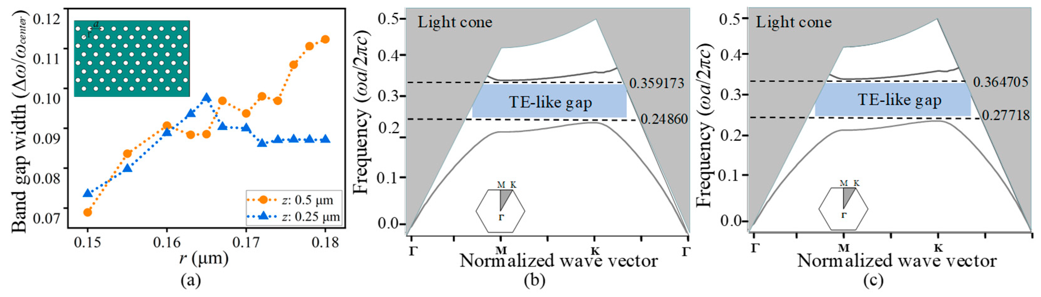
Figure 1a shows the normalized band gap width /, where is the band gap width and is the center frequency of the band gap. The normalized band gap width is given with respect to . The inset of Figure 1a can find the PhC slab prototype with structural parameter definitions, in which r is the radius of the air holes and a is the lattice constant. We keep a at 0.51 μm, z at 0.5 μm, and vary the radius value r from 0.15 μm to 0.18 μm. The normalized band gap width increases from 0.068911 to 0.116214 while we increase r. Moreover, when z is at 0.25 μm, a is at 0.515 μm, and we vary r, the normalized band gap width increases from 0.073506 to 0.087118. Based on the simulation analysis results, we obtain the optimized wide band gap for silicon-based PhC structures operating in the ~1550 nm wavelength range, as shown in Figure 1b,c. In such a case, the following structural parameters are chosen: a = 0.51 μm, r = 0.178 μm, z = 0.5 μm; and a = 0.515 μm, r = 0.178 μm, z = 0.25 μm.
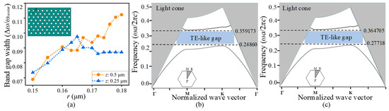
Figure 1.
Band gap characteristics of the 2D silicon-based PhC structure. (a) Normalized band gap width as a function of the hole radius. Inset shows the 2D PhC prototype with structural parameter definitions. (b,c) Optimized band gap performance for the silicon-based PhC structure with different thicknesses of 0.5 μm and 0.25 μm, respectively.
- B.
- Waveguide performance simulation: unveiling transmission characteristics
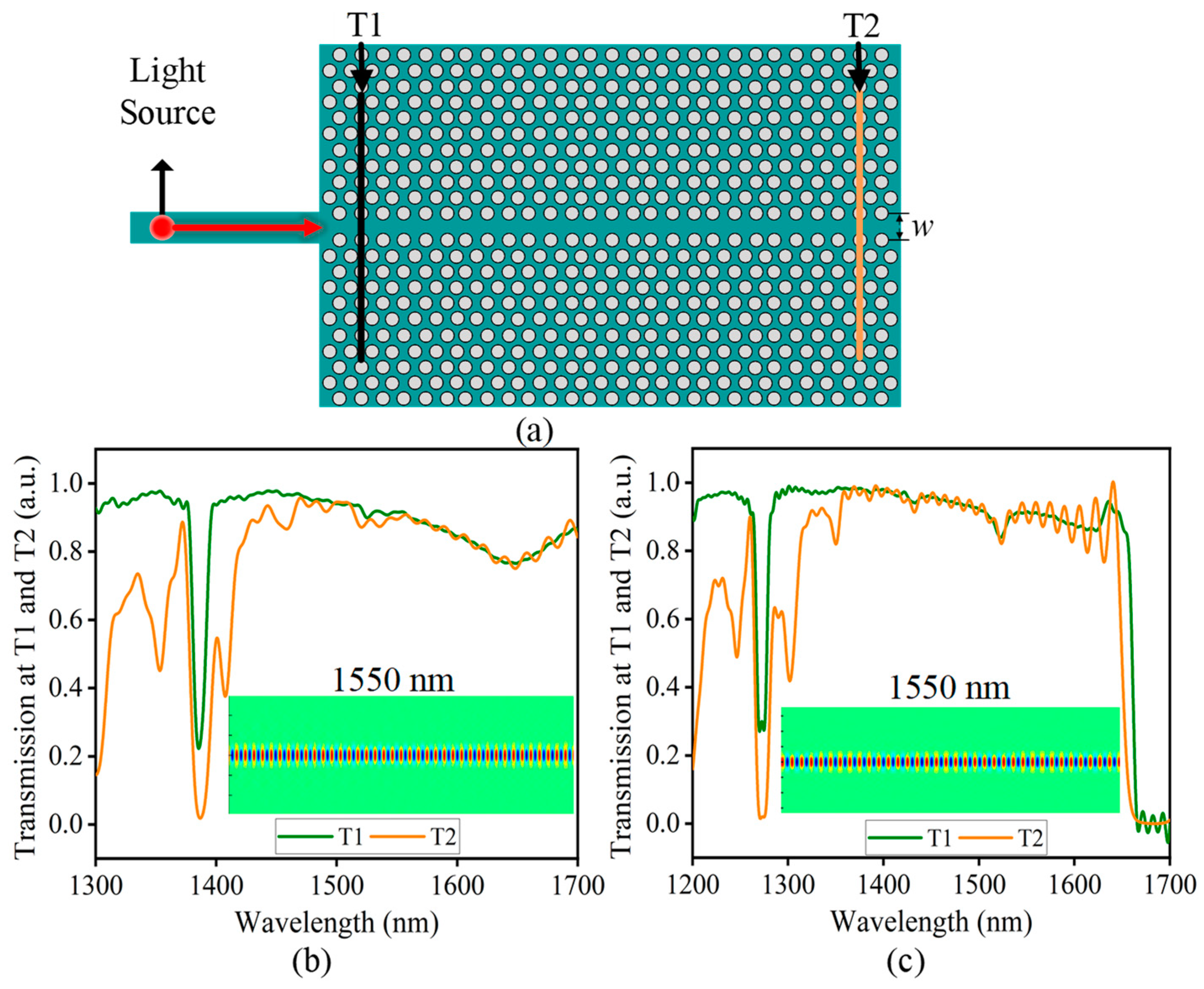
The emergence of silicon-based PhC waveguides and 2D silicon-based PhC line-defect optical cavities has revolutionized the field of integrated photonics. Silicon-based PhC waveguides provide efficient light guiding and low-loss transmission, facilitating high-speed data transmission and compact optical interconnects [43]. This section focuses on the design guidelines and characterization of silicon-based PhC waveguides for two different thicknesses. The first step in designing a silicon-based PhC waveguide involves creating the PhC slab with air holes and designing the line-defect width w to ensure it covers the required operating wavelength range (1500 nm–1630 nm). To simulate the transmission characteristics of the silicon-based PhC waveguide, a model is constructed, as depicted in Figure 2a. The figure also shows the line-defected PhC waveguide details, where an air slot is introduced at its center (represented by s) and w is defined as the distance between the centers of adjacent holes. Regularly, w = k * √3 a; here, k can be varied from 0.3 to 1.5, so the w values can vary from 0.03 μm to 0.15 μm if we set a to 0.51 μm, and s values can vary from 0.05 μm to 0.2 μm.

Figure 2.
Simulated transmission features of the designed 2D silicon-based PhC waveguides. (a) provides the simulation model employed in this study. (b,c) illustrate the transmission rates of 2D silicon-based PhC waveguides for slab thicknesses of 0.5 μm and 0.25 μm, respectively. The transmission rates are plotted as a function of the wavelength, demonstrating the waveguide’s ability to guide and transmit light efficiently within the specified thicknesses. Furthermore, the electric field distribution also shows the fundamental mode for each thickness.
In this simulation setup, the light source is placed on a straight waveguide outside the photonic crystal structure. Typically, in FDTD simulations, a monitor is placed near the end of the waveguide to measure the monitored light intensity and compare it with the light source to obtain the transmission spectrum. However, in this case, since the light source is located outside the structure, there is some energy loss when the straight waveguide couples with the PhC waveguide. To overcome this energy loss, two monitors are positioned inside the PhC waveguide, as shown in Figure 2a. One monitor, labeled T1, is placed at the beginning of the PhC waveguide, while the other monitor, labeled T2, is positioned at the end of the waveguide. The T1 monitor measures the light intensity entering the PhC waveguide, which serves as the initial light intensity. The T2 monitor measures the optical spectrum at the output, representing the output light intensity at the desired wavelength. By analyzing the transmission characteristics using the T1 and T2 monitors, we optimize the behavior of the silicon-based PhC waveguide to ensure efficient light transmission within the desired wavelength range.
In addition, the relationship between the line-defect width w and the operating wavelength of the silicon-based PhC waveguide is examined, and the corresponding findings are presented in Figure 2b,c. The simulation results presented in Figure 2b indicate that the proposed silicon-based PhC waveguide, with a line-defect width w of 0.129 μm and a slab thickness of 0.5 μm, exhibits a passband region from 1420 nm to 1700 nm. Within this range, the transmission rate varies between 75% and 94%. Notably, the transmission rate remains consistently above 89% within the C-band. In Figure 2c, considering a slab thickness of 0.25 μm and a line-defect width w of 0.133 μm, the simulation results show a passband region spanning from 1360 nm to 1620 nm. The transmission rate within this range varies between 83% and 92%. Moreover, the transmission rate remains above 90% for the entire C-band range. These findings demonstrate the potential of the proposed silicon-based PhC waveguide for achieving efficient signal transmission in fiber optic communication systems and integrated photonic circuits, particularly within specific wavelength ranges. All the simulated results are summarized in Table 1.

Table 1.
Parameters for each thickness, including the normalized band gap width /, the working wavelength range, and the transmission rates in the passband region and C-band.
- C.
- Characterization analysis of radius and line-defect waveguide width for z = 0.5 μm
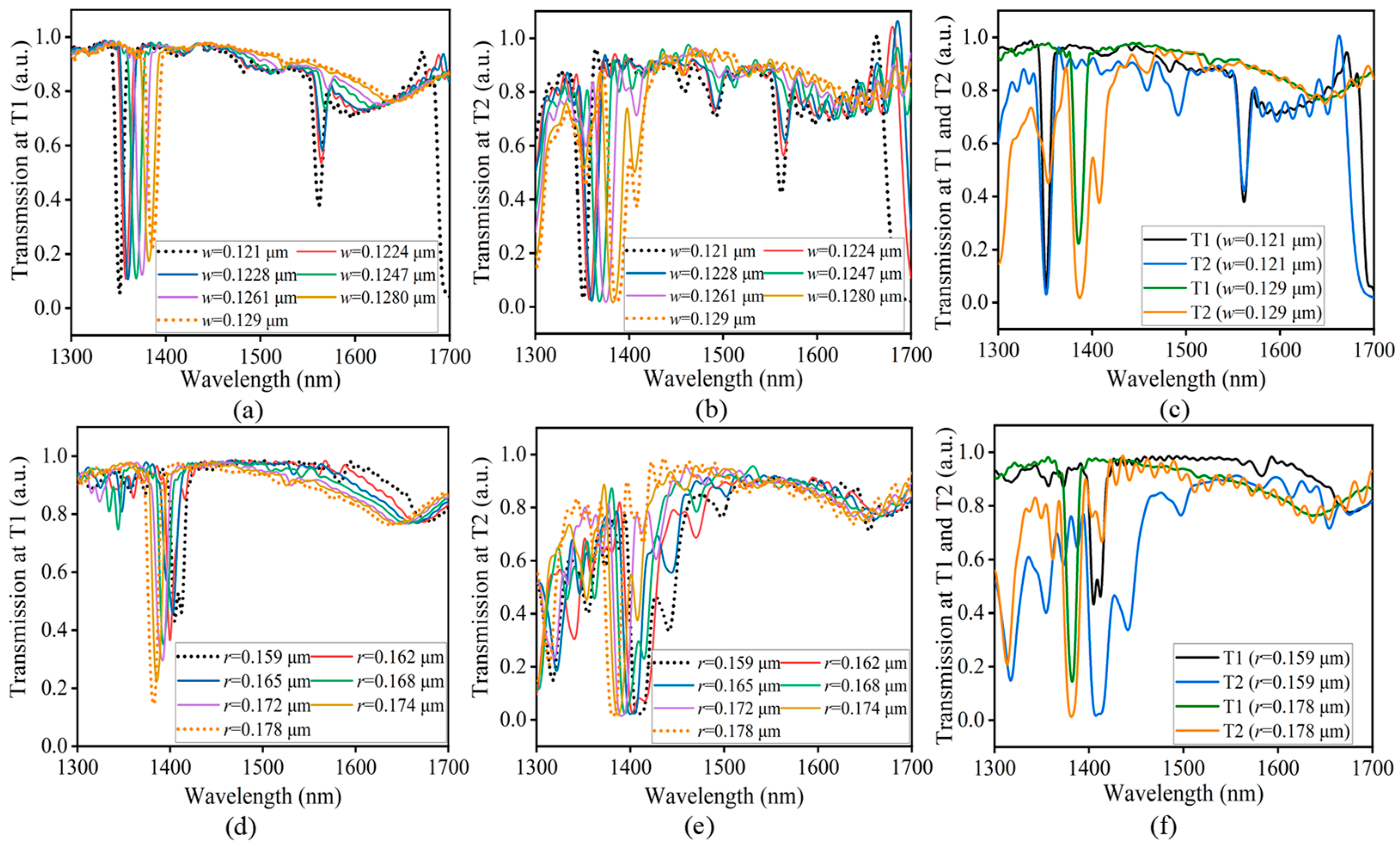
The primary objective of our study is to investigate the influence of the line-defect width w and radius r on the passband region and transmission rate. To achieve this, we conducted a systematic adjustment of the w parameter within the range of 0.121 μm to 0.129 μm. Additionally, we maintained a fixed thickness z at 0.5 μm, a at 0.51 μm, and r at 0.178 μm throughout the analysis. The results presented in Figure 3a,b illustrate the influence of adjusting w on the transmission rate and passband region of the silicon-based PhC waveguide. The optimization of w leads to an improvement in the transmission rate and expands the passband regions, as depicted in Figure 3c; also, increasing w from 0.121 μm to 0.129 μm causes a change in the cut-off wavelength from 1350 nm to 1385 nm. The parameter w is set precisely at 0.121 μm, the transmission rate is 38%, and the passband region spans from 1365 nm to 1545 nm. Further optimizing and adjusting the w value to 0.129 μm, as seen in Figure 3c, results in a broader passband region from 1430 nm to 1700 nm with an overall transmission rate of 75%.
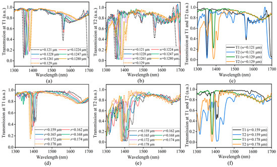
Figure 3.
Influence of w and r on the transmission rates and passband regions of 2D silicon-based PhC waveguides. (a,b) illustrate the impact of w on the transmission rates and passband region for z = 0.5 μm slab thickness. (c) depicts the comparison of w for T1 and T2. (d,e) illustrate the effect of r on transmission rates and passband region. (f) depicts the comparison of r for T1 and T2.
Figure 3d,e demonstrate the effect of r on the transmission rate and passband region, where w is constant at 0.129 μm and a at 0.51 μm. In Figure 3f, r is set at 0.159 μm, the cut-off wavelength is set at 1415 nm, and the passband region ranges from 1500 nm to 1700 nm with an overall transmission rate of 71%. Upon increasing r to 0.178 μm, the cut-off wavelength shifts from 1500 nm to 1385 nm, and the passband range expands from 1430 nm to 1700 nm, with an overall transmission rate of 75%. Within the desired wavelength range of 1500 nm to 1630 nm, the transmission rate is up to 82%.
- C.
- Characterization analysis of radius and line-defect waveguide width for z = 0.25 μm
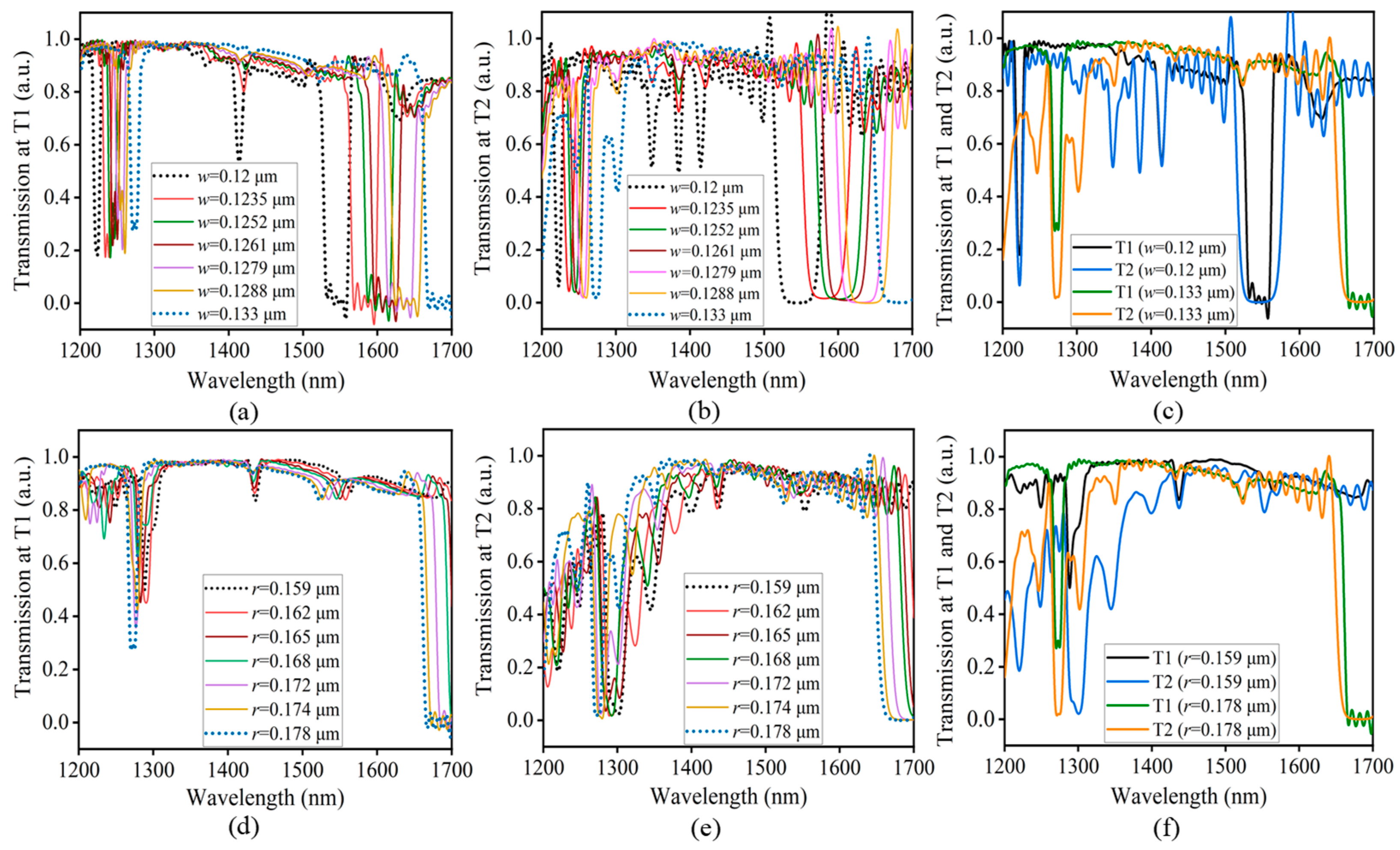
For the case of the silicon-based PhC waveguide for z at 0.25 μm, we keep a constant at 0.515 μm and r at 0.178 μm, and we observe significant performance changes by adjusting the w parameter as depicted in Figure 4a,b. Initially, w is set at 0.12 μm and the passband spans from 1225 nm to 1490 nm with an overall transmission rate of 49% and a cut-off wavelength of 1221 nm. Increasing the w value to 0.133 μm expands the passband region from 1360 nm to 1620 nm, significantly improving the transmission rate to 83% and shifting the cut-off wavelength from 1221 nm to 1360 nm, as illustrated in Figure 4c. We also investigated the impact of varying r on the transmission rate and passband region, keeping w constant at 0.133 μm and varying r from 0.159 μm to 0.178 μm, as depicted in Figure 4d,e. Specifically, Figure 4f illustrates the influences of r on the silicon-based PhC waveguide passband region and transmission properties. Initially, r was set at 0.159 μm and w at 0.133 μm. The cut-off wavelength was 1300 nm, and the passband extended from 1400 nm to 1700 nm, achieving a transmission rate of 77%. However, increasing r to 0.178 μm (while w remained at 0.133 μm) shifted the cut-off wavelength to 1270 nm and adjusted the passband to span from 1360 nm to 1620 nm, with a much-improved transmission rate of up to 83%. Within the desired wavelength range of 1500 nm to 1630 nm, the transmission rate is up to 80%.
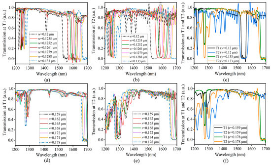
Figure 4.
Influence of w and r on the transmission rates and passband regions of 2D silicon-based PhC waveguides. (a,b) illustrate the impact of w on the transmission rates and passband region for a z of 0.25 μm slab thickness. (c) depicts the comparison of w for T1 and T2. (d,e) illustrate the effect of r on the transmission rate and passband region. (f) demonstrates the comparison of r for T1 and T2.
The simulation results of silicon-based PhC waveguides demonstrate the influence of adjusting w and r on the transmission rate and passband region for two different thicknesses of 0.5 μm and 0.25 μm. Physically, the change in w or r will affect the equivalent lattice constants of the PhC cells in the upper and lower rows, leading to a change in the band gap and, hence, the optical mode. The findings showed that adjusting w made it possible to optimize the transmission rate and passband region. Moreover, the cut-off wavelength was found to be influenced by w, while the transmission rate remained consistent regardless of specific r values. These results highlight the importance of choosing the correct waveguide dimensions to ensure optimal performance. Careful dimension selection is essential for improving waveguide efficiency and boosting signal transmission in photonic systems.
3. Investigation of High-Q 2D Silicon-Based PhC Optical Cavity
- A.
- Design Guidelines
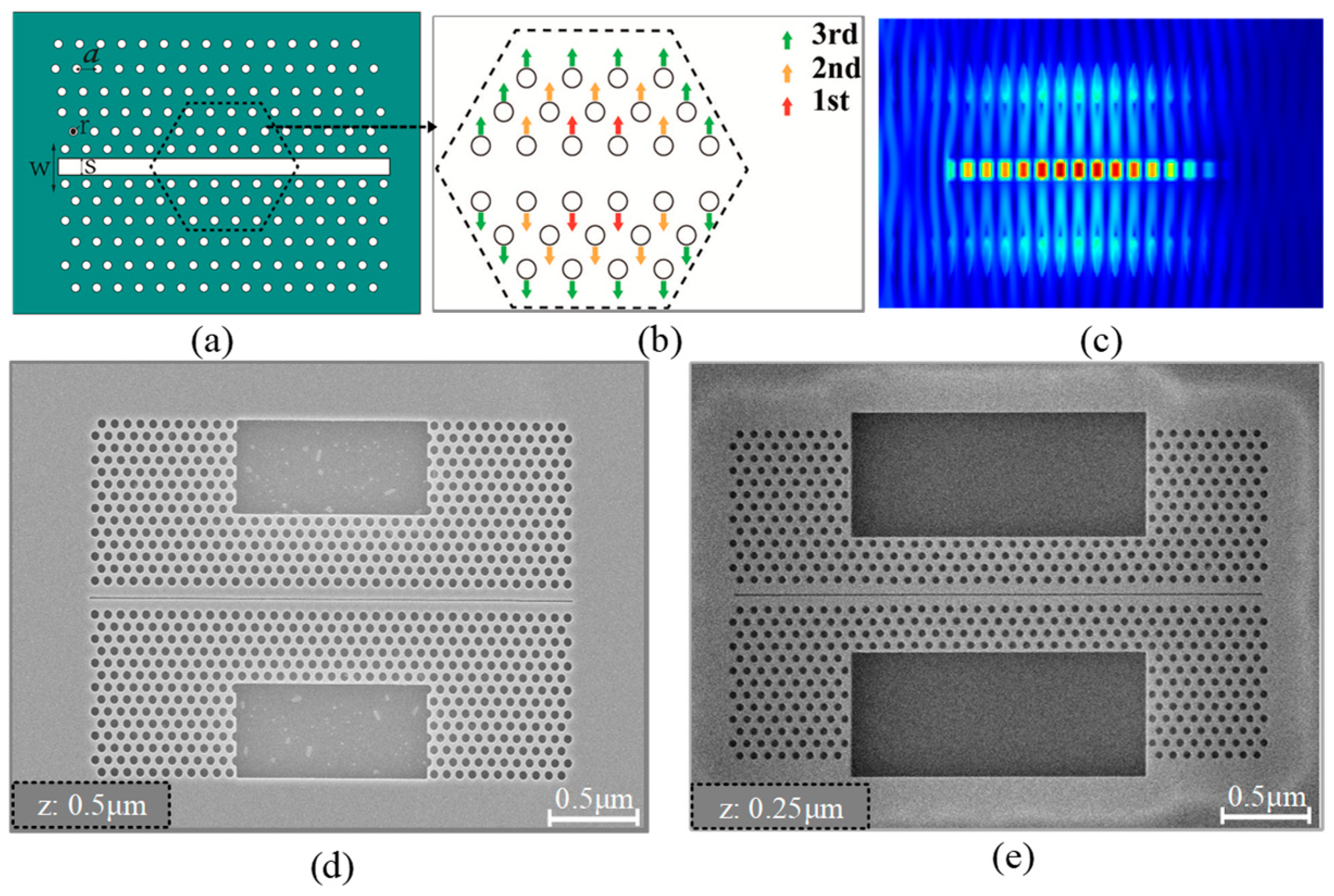
In Figure 5a,b, we can see the overview of the high-Q 2D silicon-based PhC optical cavity with hole shifts, where the hole shifts were set to 0.005 μm, 0.01 μm, and 0.015 μm in the first, second, and third directions, respectively. Specifically, the PhC cavity structure shown in Figure 5a is composed of three different air hole perturbations, a line defect, and an air slot, which is a classic cavity configuration that has been widely discussed before [45,46,47,48,49].

Figure 5.
Design principles, light confinement characteristics, and scanning electron microscope (SEM) imaging of the high-Q 2D silicon-based PhC optical cavity. (a,b) illustrate the design principles of the high-Q 2D silicon-based PhC optical cavity. (c) shows the light distribution inside the cavity. (d,e) showcase the SEM images of the high-Q 2D silicon-based PhC optical cavity device for z = 0.5 μm and z = 0.25 μm, respectively.
Controlling the resonance wavelength of an integrated PhC optical cavity is crucial for designing a cavity system that meets the requirements of various experiments and applications. The resonance wavelength is determined by factors such as w and s. By optimizing these parameters, it is possible to tune the resonance wavelength to a specific value or range of values precisely. These methods make PhC cavities a versatile and powerful tool for optical applications. We focused on optimizing the air-slot parameter s to determine the desirable wavelength for the optical mode. Additionally, we investigated the parameter w to enhance the high-Q. We employed the 2D FDTD method to simulate an integrated PhC optical cavity. In order to meet the stability conditions, the values of the space and time steps need to be extremely small, and to meet the design requirements of PhC structures, a large number of structures need to be simulated. We exploit the periodic properties of the integrated PhC cavity in the XOY plane. We use Bloch boundary conditions for the x and y directions and PML for the z direction. Figure 5c shows the simulated light distribution inside the cavity. Figure 5d,e show the SEM for silicon thicknesses of 0.5 μm and 0.25 μm, and more details will be discussed below in the Fabrication Processes for 2D Silicon-Based Integrated PhC Optical Cavity section.
- B.
- Influence of line-defect width on the Q-factor
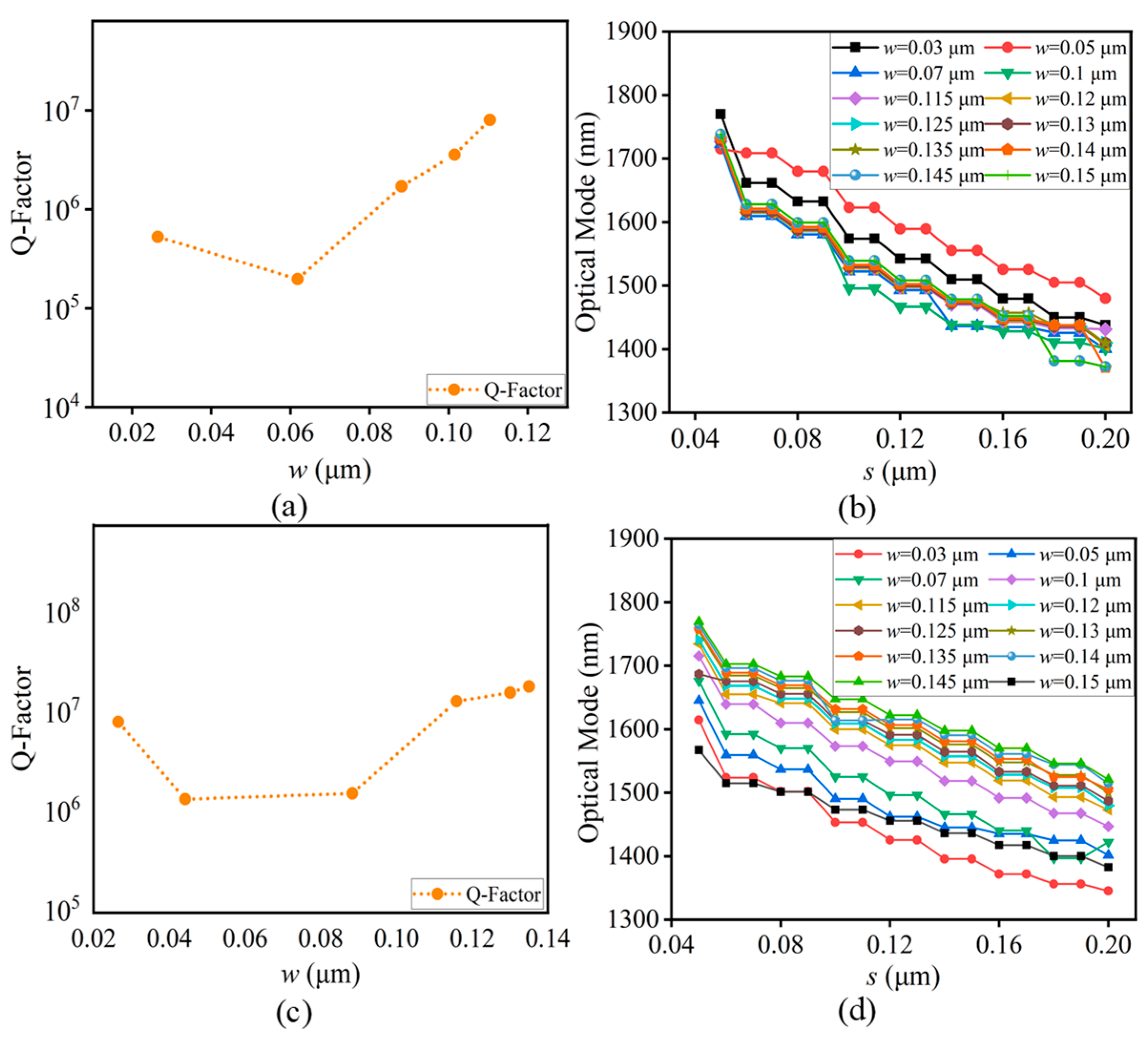
The properties of a high-Q 2D silicon-based PhC optical cavity were examined using the 2D FDTD method to simulate a 0.5 μm thickness. Figure 6a reveals a wide range of high-Q factors, spanning from 2.56 × 10⁵ to 8.01 × 10⁶ in relation to the parameter w, which varies from 0.03 μm to 0.12 μm. We kept a at 0.51 μm, r at 0.176 μm, and s at 0.1 μm. Initially, when w was set at 0.03 μm, the Q-factor was determined to be 2.56 × 10⁵, while increasing w to 0.04 μm exhibited a Q-factor of 2.1501 × 10⁵. The lowest Q-factor was due to suboptimal mode confinement and increased scattering losses, which disrupted the balance between the photonic band gap and the defect mode overlap in the PhC cavity. Upon increasing w to 0.05 μm, it exhibited a Q-factor of 5.25 × 10⁵. Further amplifying w to 0.12 μm resulted in a substantial Q-factor of 8.01 × 10⁶, accompanied by an optical mode wavelength at 1582 nm.
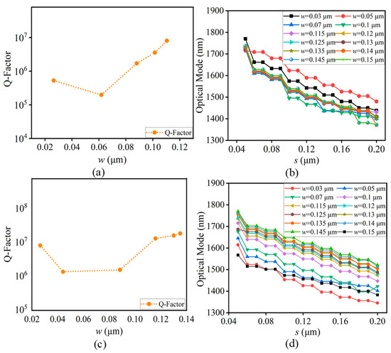
Figure 6.
Analysis of the relationship between w and the Q-factor, as well as the impact of w and s on the optical mode characteristics for different slab thicknesses. (a,c) show a simulated Q-factor concerning w for z = 0.5 μm and 0.25 μm. (b,d) show the effect of w on the optical mode along with s.
Figure 6c illustrates the impressive Q factors for a 0.25 μm thickness with a wide range from 1.4 × 10⁶ to 1.91 × 10⁷ and the variation in the parameter w within the range of 0.03 μm to 0.14 μm. It is crucial to note we set fixed values of a at 0.515 μm, r at 0.174 μm, and s at 0.1 μm throughout the simulation. Initially, when w was set at 0.03 μm, a noteworthy Q-factor of 1.4 × 10⁶ was attained, while increasing w to 0.04 μm exhibited a Q-factor of 1.2 × 10⁶. Upon increasing w to 0.1 μm, a significantly elevated Q-factor of 1.66 × 10⁷ was obtained. Further increasing w to 0.135 μm yielded a Q-factor of 1.91 × 10⁷, accompanied by an optical mode wavelength at 1571 nm. On the single transition of w for both thicknesses, the Q-factor decreased first, and then, upon increasing w further, the Q-factor increased. These findings indicate a positive correlation between the Q-factor and the increase in w, highlighting the paramount influence of these parameters on the high-Q 2D silicon-based PhC optical cavity performance. For both z thicknesses of 0.5 μm and 0.25 μm, the parameter w showcased a significant influence on the Q-factor as we increased w.
- C.
- Influence of line-defect width and air-slot width on optical mode
Figure 6b illustrates the influence of w and s on the optical mode. It is crucial to note the fixed values of a at 0.51 μm, r at 0.176 μm, and z at 0.5 μm. Initially, w is set at 0.03 μm and s varies from 0.05 μm to 0.2 μm. By examining each w value from 0.03 μm to 0.15 μm, the corresponding optical mode wavelength can be observed in Figure 6b. Initially, w is set at 0.03 μm and s is set at 0.05 μm. The optical mode wavelength is found to be at 1770.13 nm. When w is increased to 0.15 μm, the optical mode wavelength shifts to 1738.48 nm, indicating the impact of w on the optical mode wavelength. Precisely, the mode wavelength shifts about 31.65 nm. Conversely, when w is fixed at 0.03 μm and s varies from 0.05 μm to 0.2 μm, the optical mode wavelength shifts from 1770.13 nm to 1437.8 nm and the mode shift is 332.33 nm, which shows the impact of s on the optical mode wavelength. On a single transition of s from 0.05 μm to 0.06 μm, the optical mode shifts from 1770.13 nm to 1661.64 nm. Furthermore, when w is increased from 0.03 μm to 0.15 μm and s varies from 0.05 μm to 0.2 μm, the optical mode wavelength shifts from 1770.13 nm to 1372.26 nm, resulting in a shift of approximately 397.87 nm, indicating the impact of s on the optical mode wavelength.
Figure 6d illustrates the influence of w and s on the optical mode wavelength for a thickness of 0.25 μm when we fix values of a at 0.515 μm and r at 0.178 μm. Initially, s is set at 0.05 μm and w at 0.03 μm, and we have the optical mode wavelength at 1614.61 nm. Increasing w to 0.15 μm shifts the optical mode to 1567.22 nm, indicating a small impact of w on the optical mode wavelength. Precisely, the mode wavelength shifts 47.39 nm. Conversely, keeping w fixed at 0.03 μm and s varying from 0.05 μm to 0.2 μm, the optical mode wavelength shifts from 1614.61 nm to 1345.3 nm. The mode shift is about 269.31 nm, which shows a much larger impact. On a single transition of s from 0.05 μm to 0.06 μm, the optical mode shifts from 1614.61 nm to 1523.91 nm. Furthermore, when w is increased from 0.03 μm to 0.15 μm and s varies from 0.05 μm to 0.2 μm, the optical mode wavelength shifts from 1567.22 nm to 1382.67 nm. Precisely, the mode wavelength shifts about 184.55 nm, demonstrating the influence of s on the optical mode wavelength. Comparing the two different thicknesses, z values of 0.5 μm and 0.25 μm, it is observed that the impact of w on the optical modes is less significant, while s has a greater effect on the optical mode wavelength.
As mentioned before, to perform these simulations, the FDTD method was employed with a high level of mesh and accuracy to ensure precise results. However, it is essential to note that this high accuracy comes at the expense of increased computation time and memory usage. Nonetheless, it is crucial to effectively compare the experimental results with the fabricated structure. Overall, the investigation demonstrated the potential of a high-Q 2D silicon-based PhC optical cavity for use in optical applications. By optimizing w and s, it is possible to achieve a high-Q and a desirable optical mode wavelength, which are important properties for optical devices such as filters and sensors.
4. Fabrication Processes for 2D Silicon-Based Integrated PhC Optical Cavity
- A.
- Two-dimensional silicon-based PhC optical cavity integrated with silicon-based PhC waveguide
One of the significant challenges in fabricating a high-Q 2D silicon-based PhC optical cavity with an integrated PhC waveguide and silicon waveguide chip is the protection of the oxide layer at the bottom of the waveguide during the dry HF gas etching process for the oxide layer release. If the waveguide is left unprotected, it is at risk of collapse. To address this problem, we use a magnesium fluoride deposition technique to protect the waveguide. The process begins with the spin-coating of the photoresist onto the chip, followed by the development of the photoresist in the waveguide region using a mask plate. Subsequently, magnesium fluoride is deposited uniformly across the chip. As the waveguide region remains outside the photoresist, we can physically remove the magnesium fluoride from this area, thereby achieving the desired protection. The magnesium fluoride deposited on the photoresist outside the waveguide region can also be peeled off, ensuring protection of the waveguide region. Notably, the refractive index of magnesium fluoride (1.38) is similar to that of silica, which minimizes its impact on waveguide transmittance. Overall, this comprehensive fabrication process successfully created the desired 2D silicon-based integrated PhC optical cavity structure, meeting the design specifications and ensuring functionality within the desired wavelength range.
- B.
- Etching processing problems with solution
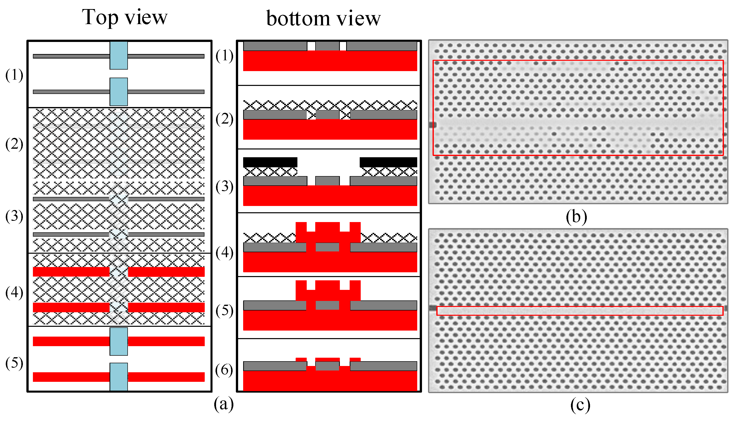
During the etching process of the top silicon structure, the PhC small holes and air slots are incredibly small, measuring in the nanometer scale. To achieve such precise dimensions, electron-beam lithography (EBL) is employed. This technique involves using a focused electron beam to scan and draw custom shapes on an electron-sensitive film coated with resist. One notable advantage of EBL is its ability to create custom patterns with a resolution of less than 10 nm, eliminating the need for a mask plate. However, it should be noted that EBL has a long etching time, making it primarily suitable for the production of photomasks and low-volume semiconductor device manufacturing for research and development purposes. When dealing with PhC structures and aiming for small resolution sizes, a challenge arises in the form of omitting certain PhC vias and air slots during the writing process, as depicted in Figure 7b,c. This issue can be attributed to the electron-beam proximity effect. Essentially, the scattering effect of the electron beam on the substrate and resist causes electron impacts in the collar region, resulting in alterations to the final structure pattern. To address this, several measures can be taken. These include controlling the exposure dose, implementing the gas-assisted self-assembly of hybrid organic–inorganic thin films (GHOST) method of secondary exposure, and considering the proximity effect during the initial layout design. By incorporating these strategies, it is possible to ensure that the pattern produced after exposure closely aligns with the original design requirements. Additionally, adjustments can be made to the design layout itself to correct any deviations, ultimately achieving the desired processing outcome.
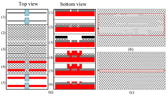
Figure 7.
Comprehensive overview of the fabrication steps involved in creating PhC structures. (a) illustrates the fabrication process with top and bottom views; (b,c) present the SEM images of PhC etching defects, indicating the leakage of engraved air vias and air grooves.
5. Experimental Setup and Measurement Results
- A.
- Experimental setup
Figure 8 shows an experimental setup to investigate the 2D silicon-based integrated PhC optical cavity. This setup utilizes a fiber coupling technique to facilitate this study. The process begins with a tunable laser, which is essential for exploring various resonance conditions in the 2D silicon-based integrated PhC optical cavity. In our measurements, we used the TSL-570 type H tunable laser with a linewidth of about 100 kHz, which is a high-performance model with over 20 dBm peak optical output power. Its advanced optical cavity design ensures picometer accuracy and sub-picometer resolution, with high-speed scanning up to 200 nm/second.
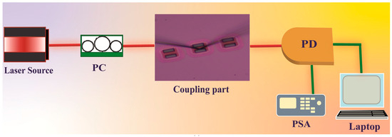
Figure 8.
An overview of the experimental setup used for testing the operational characteristics of the 2D silicon-based integrated PhC optical cavity.
The laser’s output goes through a fiber polarization controller (PC) to adjust the light’s polarization, aligning it with the 2D silicon-based integrated PhC optical cavity to maximize coupling efficiency. Subsequently, the test device is coupled using side-feed coupling with specially prepared fiber optic cones, precisely aligned with the waveguide to effectively excite the optical resonance modes within the 2D silicon-based integrated PhC optical cavity. Accurate alignment is crucial for studying the resonance characteristics. The light emerging from the cavity is directed to a photodetector (PD) selected for its lower frequency response to match the relevant resonance modes. The photodetector converts the optical signals into electrical signals, which are then processed by a data acquisition (DAQ) system to digitize them. The DAQ system ensures precise measurements of the resonance characteristics, such as wavelength shifts and intensity variations. Finally, the digitized data are analyzed on a computer. This analysis involves a detailed examination of the resonance characteristics, including Q factors, mode spectra, and resonance wavelengths, allowing for a thorough understanding of light behavior within the 2D silicon-based integrated PhC optical cavity. This experimental setup is crucial for advancing the understanding and development of photonic devices, with significant applications in optical communications and sensing.
- B.
- Optical properties
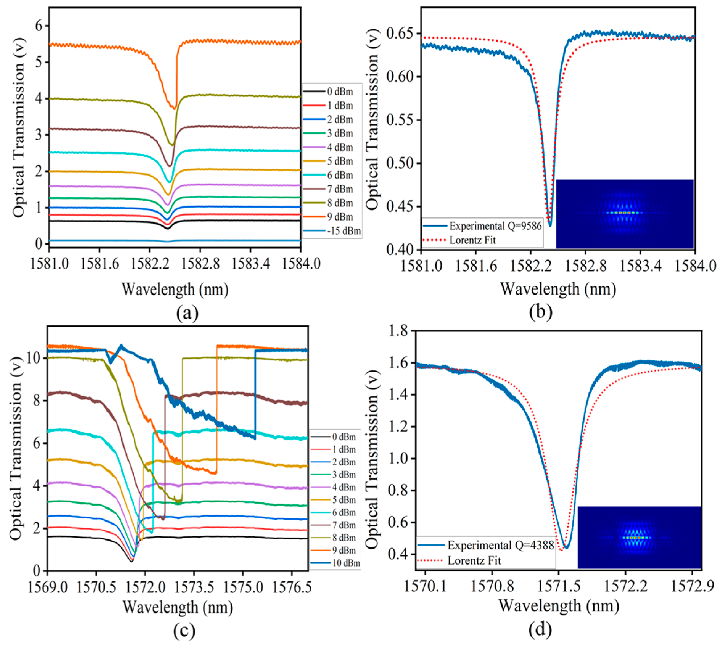
To examine the optical properties of the device, experimental tests are conducted for the 2D silicon-based integrated PhC optical cavity with a thickness of z at 0.5 µm. The optical transmission measured under different pump laser input powers is shown in Figure 9a. Figure 9b shows the resonant wavelength of the fundamental mode located at 1582 nm, which agrees with the expected high-Q mode predicted by the simulation results. The theoretical Q-factor for this mode surpasses 8.01 × 10⁶. However, the measured high-Q-value was obtained at 9586, by fitting the experimental data using a Lorentz function. The electric field intensity distribution of the fundamental mode exhibits for z at 0.5 µm, and a concentration of the highest field intensity at the center of the cavity within the air slot is shown in Figure 9b. This outcome agrees with the anticipated characteristics of the field distribution for this cavity.

Figure 9.
Optical transmission curves of different power levels from the laser source for the 2D silicon-based integrated PhC optical cavity. (a,c) are the measured optical transmission, showcasing its variation with different power levels from the laser source. (b,d) are the optical Q-factors measured and presented, accompanied by the corresponding electric field distributions.
Additionally, similar experimental tests were conducted for a two-dimensional silicon-based integrated PhC optical cavity with a thickness of 0.25 µm. The optical transmission under various pump laser input powers is presented in Figure 9c. The resonant wavelength of the fundamental mode was determined to be 1571 nm, which matched the high-Q mode predicted by the simulations. For this configuration, the theoretical Q-factor was estimated to exceed 1.91 × 10⁷. Nevertheless, the measured high-Q-value, obtained by fitting the experimental data with a, Lorentz function, was found to be 4388.
To determine the light intensity irradiated in the cavity, we use the formula P3 = √(P1 * P2), where P1 is the power of the laser source and P2 is the power reaching the photodetector. In Figure 9c, we observe that the optical transmission exhibits a sharp curve when the laser power reaches 9 dBm, corresponding to an intracavity power of approximately 56.3 µW. In contrast, at 1 dBm laser power, the intracavity power is approximately 1.387 µW. The electric field intensity distribution of the cavity mode for z at 0.25 µm is shown in Figure 9d, indicating a concentration of the highest field intensity at the center of the cavity within the air slot. This outcome agrees with the anticipated characteristics of the field distribution for this cavity. Table 2 illustrates a comparison of the theoretical optical Q-factors for different optical cavities or structures.
Table 2.
Comparison of the theoretical optical Q-factors for different optical cavities or structures.
Moreover, as shown in Figure 9c for z at 0.25 μm, when increasing the pump laser power from −0 dBm to 10 dBm, the resonance wavelength of the fundamental mode is dragged from 1571.5 nm to 1575.5 nm, which is 4 nm. As noted, this shift is attributed to the heating of the PhC cavity structure. Increased input power raises the cavity temperature, altering the refractive index of the material through the thermo-optic effect and thus resulting in a resonant wavelength shift. To provide a more detailed analysis, we estimated the cavity temperature for different input power levels. The relation between the wavelength shift and the temperature change can be expressed as follows:
where is the initial resonant wavelength and is the thermo-optic coefficient of the material. For silicon, the thermo-optic coefficient is approximately . Using our experimental data, we calculated the temperature increase for various input power levels. The results are summarized in Table 3.
Table 3.
Relationship between input power, wavelength shift, and estimated temperature increase for the experiment.
The 2D silicon-based integrated PhC optical cavity exhibits a remarkable capability to confine light within its structure, resulting in a substantial accumulation of photons in its designated cavity region. This high degree of light confinement serves as a crucial attribute of the 2D silicon-based integrated PhC optical cavity, allowing it to efficiently capture and harness a large number of photons. As we gradually escalate the intensity of the input laser, a fascinating optical phenomenon known as optical bistable nonlinearity manifests itself. This captivating occurrence arises due to the inherent thermal nonlinearity present in the material. The interaction between the intense laser beam and the material induces a nonlinear response, triggering a shift in the resonant wavelength of the 2D silicon-based integrated PhC optical cavity. Specifically, this shift leads to a gradual transition of the resonant frequency towards longer wavelengths.
6. Conclusions
Our research highlights the importance of design optimization and fabrication techniques to achieve high-Q optical devices using PhC and silicon-based structures. We successfully designed and fabricated a high-Q 2D silicon-based PhC optical cavity with integrated waveguides. By optimizing the line-defect width and air-slot width, we achieved remarkable Q-factors of 8.01 × 10⁶ and 1.91 × 10⁷ for silicon thicknesses of 0.5 μm and 0.25 μm, respectively, which are the highest theoretical Q-factors to our knowledge [45,49,50,51,52]. The line-defect width and air-slot width played a crucial role in determining thehigh-Q, optical mode wavelength, and linewidth. Moreover, we demonstrated the successful fabrication of the devices using EBL; the measured high-Q for a silicon thickness of 0.5 μm was 9586, and for a silicon thickness of 0.25 μm was 4388. Further investigations are required to understand and improve the experimental Q-factor, potentially through optimizing coupling processes.
Additionally, we investigated the design guidelines and working principles of silicon-based PhC waveguides. By varying the waveguide line-defect widths and radii, we analyzed the transmission rate and passband region for silicon thicknesses of 0.5 μm and 0.25 μm. The simulation results showed impressive transmission rates of 75% for a silicon thickness of 0.5 μm and 83% for a silicon thickness of 0.25 μm across various passband regions, including the entire C-band region. The transmission rate increased to 89% and 90%, demonstrating the potential of the silicon-based PhC waveguide for efficient light transmission. Overall, our research findings contribute to understanding PhC devices and silicon-based structures, highlighting their capability to achieve high-Q optical devices. These findings have implications for integrated photonics applications and emphasize the significance of design optimization and fabrication techniques in realizing advanced optical systems.
Author Contributions
Conceptualization, S.M. and Y.H.; methodology, S.M. and D.C.; software, D.C.; validation, D.C., J.Z. and Z.L. (Zhe Li); investigation, S.M. and C.X.; writing—original draft preparation, S.M.; writing—review and editing, S.M., P.K., Z.L. (Zhongke Lei) and Y.H.; supervision, G.W. All authors have read and agreed to the published version of the manuscript.
Funding
This work was supported in part by the National Natural Science Foundation of China (project contract nos. 62371106, U2230206, and 62204264), in part by the National Key R&D Program (project contract no. 2022YFA1405900), in part by the Sichuan Provincial Science and Technology Planning Program (project contract nos. 2022YFG0230 and 2023YFG0040), in part by the Joint Fund of ZF and the Ministry of Education (grant no. 8091B022126), in part by the Fundamental Enhancement Program Technology Area Fund (grant no. 2021-JCJQ-JJ-0667), in part by the China Postdoctoral Science Foundation (project contract no. 2023M740534), and in part by the Innovation Ability Construction Project for Sichuan Provincial Engineering Research Center of Communication Technology for Intelligent IoT (2303-510109-04-03-318020).
Institutional Review Board Statement
Not applicable.
Informed Consent Statement
Not applicable.
Data Availability Statement
The data will be made available on request.
Conflicts of Interest
Authors Jun Zhou, Zhongke Lei were employed by the company Sichuan Guoruan Technology Group Co., Ltd. The remaining authors declare that the research was conducted in the absence of any commercial or financial relationships that could be construed as a potential conflict of interest.
References
- Ghatak, A.K.; Thyagarajan, K. An Introduction to Fiber Optics; Cambridge University Press: Cambridge, UK, 1998. [Google Scholar]
- Gorodetsky, M.L.; Savchenkov, A.A.; Ilchenko, V.S. Ultimate Q of optical microsphere resonators. Opt. Lett. 1996, 21, 453–455. [Google Scholar] [CrossRef] [PubMed]
- Meade, R.D.V.; Johnson, S.G.; Winn, J.N. Photonic Crystals: Molding the Flow of Light; Princeton University Press: Princeton, NJ, USA, 2008. [Google Scholar]
- Little, B.E.; Chu, S.T.; Haus, H.A.; Foresi, J.; Laine, J.-P. Microring resonator channel dropping filters. J. Light. Technol. 1997, 15, 998–1005. [Google Scholar] [CrossRef]
- Vahala, K.J. Optical microcavities. Nature 2003, 424, 839–846. [Google Scholar] [CrossRef] [PubMed]
- Boyd, J.A.; Lahaye, T. A basic introduction to ultrastable optical cavities for laser stabilization. Am. J. Phys. 2024, 92, 50–58. [Google Scholar] [CrossRef]
- Faraon, A.; Santori, C.; Huang, Z.; Acosta, V.M.; Beausoleil, R.G. Coupling of nitrogen-vacancy centers to photonic crystal cavities in monocrystalline diamond. Phys. Rev. Lett. 2012, 109, 033604. [Google Scholar] [CrossRef] [PubMed]
- Xu, Q.; Schmidt, B.; Pradhan, S.; Lipson, M. Micrometre-scale silicon electro-optic modulator. Nature 2005, 435, 325–327. [Google Scholar] [CrossRef] [PubMed]
- Hadjaj, F.; Belghachi, A.; Halmaoui, A.; Belhadj, M.; Mazouz, H. Study of a Fabry-Perot resonator. Int. J. Phys. Math. Sci. 2013, 7, 1713–1717. [Google Scholar]
- He, L.; Özdemir, Ş.K.; Yang, L. Whispering gallery microcavity lasers. Laser Photonics Rev. 2013, 7, 60–82. [Google Scholar] [CrossRef]
- Zhang, X.; Liu, B.; Zhou, X.; Yan, X.; Wang, F.; Yu, Z.; Cheng, T. Generalized Perturbation Theory for Weakly Deformed Microdisk Cavities. Adv. Phys. Res. 2024, 3, 2300105. [Google Scholar] [CrossRef]
- Li, X.; Cui, B.; Xu, P.; Xie, Y.; Wang, P.; Tong, L.; Guo, X. Ice Microsphere Optical Cavities. Adv. Opt. Mater. 2024, 12, 2302609. [Google Scholar] [CrossRef]
- Kavokin, A.V.; Baumberg, J.J.; Malpuech, G.; Laussy, F.P. Microcavities; Oxford University Press: Oxford, UK, 2017; Volume 21. [Google Scholar]
- Cheben, P.; Halir, R.; Schmid, J.H.; Atwater, H.A.; Smith, D.R. Subwavelength integrated photonics. Nature 2018, 560, 565–572. [Google Scholar] [CrossRef]
- Pust, O. Optical filters–Technology and applications. In Portable Spectroscopy and Spectrometry; Wiley Online Library: Hoboken, NJ, USA, 2021; pp. 147–177. [Google Scholar]
- Liu, K.; Ye, C.R.; Khan, S.; Sorger, V.J. Review and perspective on ultrafast wavelength-size electro-optic modulators. Laser Photonics Rev. 2015, 9, 172–194. [Google Scholar] [CrossRef]
- Hesmer, F.; Tatartschuk, E.; Zhuromskyy, O.; Radkovskaya, A.A.; Shamonin, M.; Hao, T.; Stevens, C.J.; Faulkner, G.; Edwards, D.J.; Shamonina, E. Coupling mechanisms for split ring resonators: Theory and experiment. Phys. Status Solidi B 2007, 244, 1170–1175. [Google Scholar] [CrossRef]
- Ferreira, M.F.; Castro-Camus, E.; Ottaway, D.J.; López-Higuera, J.M.; Feng, X.; Jin, W.; Jeong, Y.; Picqué, N.; Tong, L.; Reinhard, B.M. Roadmap on optical sensors. J. Opt. 2017, 19, 083001. [Google Scholar] [CrossRef] [PubMed]
- Gan, L.; Li, Z. Photonic crystal cavities and integrated optical devices. Sci. China Phys. Mech. Astron. 2015, 58, 114203. [Google Scholar] [CrossRef]
- Yard, P.; Jones, A.E.; Paesani, S.; Maïnos, A.; Bulmer, J.F.; Laing, A. On-chip quantum information processing with distinguishable photons. Phys. Rev. Lett. 2024, 132, 150602. [Google Scholar] [CrossRef] [PubMed]
- Zain, A.R.M.; Richard, M. Modelling of photonic crystal (PhC) cavities: Theory and applications. In Photonic Crystals-A Glimpse of the Current Research Trends; IntechOpen: London, UK, 2019. [Google Scholar]
- Talebzadeh, R.; Soroosh, M.; Mehdizadeh, F. Improved low channel spacing high quality factor four-channel demultiplexer based on photonic crystal ring resonators. Opt. Appl. 2016, 46, 553–564. [Google Scholar]
- Agrawal, G.P. Optical communication: Its history and recent progress. In Optics Our Time; The Institute of Optics, University of Rochester: Rochester, NY, USA, 2016; pp. 177–199. [Google Scholar]
- Elsherif, M.; Salih, A.E.; Muñoz, M.G.; Alam, F.; AlQattan, B.; Antonysamy, D.S.; Zaki, M.F.; Yetisen, A.K.; Park, S.; Wilkinson, T.D. Optical fiber sensors: Working principle, applications, and limitations. Adv. Photonics Res. 2022, 3, 2100371. [Google Scholar] [CrossRef]
- Alaee, R.; Vaddi, Y.; Boyd, R.W. Dynamic coherent perfect absorption in nonlinear metasurfaces. Opt. Lett. 2020, 45, 6414–6417. [Google Scholar] [CrossRef]
- O’brien, J.L.; Furusawa, A.; Vučković, J. Photonic quantum technologies. Nat. Photonics 2009, 3, 687–695. [Google Scholar] [CrossRef]
- Tanabe, T.; Notomi, M.; Kuramochi, E.; Shinya, A.; Taniyama, H. Trapping and delaying photons for one nanosecond in an ultrasmall high-Q photonic-crystal nanocavity. Nat. Photonics 2007, 1, 49–52. [Google Scholar] [CrossRef]
- Fushimi, A.; Taniyama, H.; Kuramochi, E.; Notomi, M.; Tanabe, T. Fast calculation of the quality factor for two-dimensional photonic crystal slab nanocavities. Opt. Express 2014, 22, 23349–23359. [Google Scholar] [CrossRef] [PubMed]
- Baba, T. Photonic Integration Based on Si Photonics and Photonic Crystals. In Proceedings of the 2021 Opto-Electronics and Communications Conference (OECC), Hong Kong, China, 3–7 July 2021; pp. 1–3. [Google Scholar]
- Jokar, M.H.; Naraghi, A.; Seifouri, M.; Olyaee, S. Design of bio-alcohol sensor based on waveguide-coupled photonic crystal cavity. Results Opt. 2023, 13, 100563. [Google Scholar] [CrossRef]
- Shekhar, S.; Bogaerts, W.; Chrostowski, L.; Bowers, J.E.; Hochberg, M.; Soref, R.; Shastri, B.J. Roadmapping the next generation of silicon photonics. Nat. Commun. 2024, 15, 751. [Google Scholar] [CrossRef]
- Krauss, T.F. Slow light in photonic crystal waveguides. J. Phys. D Appl. Phys. 2007, 40, 2666. [Google Scholar] [CrossRef]
- Baba, T. Slow light in photonic crystals. Nat. Photonics 2008, 2, 465–473. [Google Scholar] [CrossRef]
- Notomi, M.; Kuramochi, E.; Taniyama, H. Ultrahigh-Q nanocavity with 1D photonic gap. Opt. Express 2008, 16, 11095–11102. [Google Scholar] [CrossRef]
- Miri, M.; Khavasi, A.; Miri, M.; Mehrany, K. A transmission line resonator model for fast extraction of electromagnetic properties of cavities in two-dimensional photonic crystals. IEEE Photonics J. 2010, 2, 677–685. [Google Scholar] [CrossRef]
- Chen, D.; Muhammad, S.; Huang, W.; Zheng, X.; Wen, G.; Huang, Y. Parameter investigations on lithium-niobate-based photonic crystal optomechanical cavity. Results Phys. 2023, 48, 106458. [Google Scholar] [CrossRef]
- Lu, J.; Zhou, S.; Wu, Y.; Yu, H. Two-dimensional thin film lithium niobate photonic crystal waveguide for integrated photonic chips. Appl. Phys. Lett. 2024, 124, 141104. [Google Scholar] [CrossRef]
- Joannopoulos, J.D.; Meade, R.D.; Winn, J.N.; Russell, P.S.J. Photonic crystals: Molding the flow of light. Nature 1996, 381, 290. [Google Scholar]
- Brillouin, L. Wave Propagation in Periodic Structures; Dover Pubns: New York, NY, USA, 1946. [Google Scholar]
- Sakoda, K.; Sakoda, K. Optical Properties of Photonic Crystals; Springer: Berlin/Heidelberg, Germany, 2005; Volume 2. [Google Scholar]
- Zhang, X.; Liu, Z. Superlenses to overcome the diffraction limit. Nat. Mater. 2008, 7, 435–441. [Google Scholar] [CrossRef] [PubMed]
- Minkov, M.; Savona, V.; Gerace, D. Photonic crystal slab cavity simultaneously optimized for ultra-high Q/V and vertical radiation coupling. Appl. Phys. Lett. 2017, 111, 131104. [Google Scholar] [CrossRef]
- Gangwar, R.K.; Pathak, A.K.; Kumar, S. Recent progress in photonic crystal devices and their applications: A review. Photonics 2023, 10, 1199. [Google Scholar] [CrossRef]
- HBanaei, A.; Serajmohammadi, S.; Mehdizadeh, F.; Andalib, A. Band Gap Properties of Two-Dimensional Photonic Crystal Structures with Rectangular Lattice. J. Opt. Commun. 2015, 36, 109–114. [Google Scholar] [CrossRef]
- Yamamoto, T.; Notomi, M.; Taniyama, H.; Kuramochi, E.; Yoshikawa, Y.; Torii, Y.; Kuga, T. Design of a high-Q air-slot cavity based on a width-modulated line-defect in a photonic crystal slab. Opt. Express 2008, 16, 13809–13817. [Google Scholar] [CrossRef] [PubMed]
- Tanaka, Y.; Asano, T.; Akahane, Y.; Song, B.-S.; Noda, S. Theoretical investigation of a two-dimensional photonic crystal slab with truncated cone air holes. Appl. Phys. Lett. 2003, 82, 1661–1663. [Google Scholar] [CrossRef]
- Shen, M.; Xie, J.; Zou, C.-L.; Xu, Y.; Fu, W.; Tang, H.X. High frequency lithium niobate film-thickness-mode optomechanical resonator. Appl. Phys. Lett. 2020, 117, 131104. [Google Scholar] [CrossRef]
- Boes, A.; Corcoran, B.; Chang, L.; Bowers, J.; Mitchell, A. Status and potential of lithium niobate on insulator (LNOI) for photonic integrated circuits. Laser Photonics Rev. 2018, 12, 1700256. [Google Scholar] [CrossRef]
- Li, Y.; Zheng, J.; Gao, J.; Shu, J.; Aras, M.S.; Wong, C.W. Design of dispersive optomechanical coupling and cooling in ultrahigh-Q/V slot-type photonic crystal cavities. Opt. Express 2010, 18, 23844–23856. [Google Scholar] [CrossRef]
- Dharanipathy, U.P.; Minkov, M.; Tonin, M.; Savona, V.; Houdré, R. High-Q silicon photonic crystal cavity for enhanced optical nonlinearities. Appl. Phys. Lett. 2014, 105, 101101. [Google Scholar] [CrossRef]
- Li, M.; Liang, H.; Luo, R.; He, Y.; Lin, Q. High-Q 2D lithium niobate photonic crystal slab nanoresonators. Laser Photonics Rev. 2019, 13, 1800228. [Google Scholar] [CrossRef]
- Ge, R.; Yan, X.; Liang, Z.; Li, H.; Wu, J.; Liu, X.; Chen, Y.; Chen, X. Large quality factor enhancement based on cascaded uniform lithium niobate bichromatic photonic crystal cavities. Opt. Lett. 2023, 48, 113–116. [Google Scholar] [CrossRef] [PubMed]

Disclaimer/Publisher’s Note: The statements, opinions and data contained in all publications are solely those of the individual author(s) and contributor(s) and not of MDPI and/or the editor(s). MDPI and/or the editor(s) disclaim responsibility for any injury to people or property resulting from any ideas, methods, instructions or products referred to in the content. |
© 2024 by the authors. Licensee MDPI, Basel, Switzerland. This article is an open access article distributed under the terms and conditions of the Creative Commons Attribution (CC BY) license (https://creativecommons.org/licenses/by/4.0/).