Abstract
Directional coupling of light at the nanoscale plays a significant role in both fundamental research and practical applications, which are crucial for the development of on-chip photonic devices. In this work, we propose a broadband directional coupler for surface plasmon polaritons (SPPs) utilizing a pair of obliquely perforated nanoslits. We demonstrate that tilting the slits significantly enhances the sensitivity of plasmonic coupling phase variation to the wavelength of the incident light, enabling precise wavelength-dependent control over SPP propagation. By optimizing the width and tilting angle of each nanoslit, we achieve an extinction ratio exceeding 10 dB with a bandwidth exceeding 400 nm and a maximum unidirectional transmission of up to 30 dB. This broadband directional SPP coupler presents a promising platform for the design and fabrication of integrated plasmonic circuits and high-performance optical devices and sensors.
1. Introduction
The integration and miniaturization of on-chip photonic devices are crucial for meeting the growing demand for higher speed, increased capacity, and improved efficiency in information acquisition, processing, and storage. Many advances have been made to enable ultra-compact devices such as waveguides, photonic crystals, nano-antennas, and meta-surfaces [1,2,3,4,5,6,7,8,9,10,11,12]. Among the numerous approaches, the employment of two-dimensional surface electromagnetic waves like surface plasmon polaritons (SPPs) has been particularly intriguing and widely investigated due to their ability to confine light to subwavelength dimensions and support a wide range of optical functionalities. Traditional SPP generators, such as prism and grating, are too large for high density integration, and plasmonic nanostructures have emerged. Many typical plasmonic devices were proposed, including light emitters [13,14], SPP emitters [15], photodetectors [16], modulators [17,18,19], biosensors [20,21], lenses [22,23], and demultiplexers [24]. A directional coupler is one of the most important plasmonic devices to launch SPP fields at desired propagating direction. To achieve this, asymmetry is introduced in either incident light [25,26] or nanostructures [27,28,29,30,31,32,33,34,35,36,37], which results in direction-dependent interference of SPP. While many efforts have been devoted to realizing the highly efficient directional coupling of plasmonic field, the operating wavelength is always limited to a narrow band due to the fixed coupling phase of the resonant element. There is a balance between the extinction ratio and bandwidth.
In this work, we introduce a novel broadband directional coupler for surface plasmon polaritons (SPPs) based on a pair of obliquely oriented nanoslits. By strategically tilting the slits, we demonstrate a significant enhancement in the sensitivity of the plasmonic coupling phase to variations in incident light wavelength. This heightened sensitivity empowers precise wavelength-dependent control over the propagation direction of the excited SPPs. Through optimization of the width and tilt angle of each nanoslit, we achieve a remarkable directional coupling performance. The ratio of SPP excitation in opposite directions, quantified by the extinction ratio, surpasses 10 dB across a broad bandwidth exceeding 400 nm, encompassing both the visible and near-infrared spectral regions. This broadband directional SPP coupler presents a promising foundation for the advancement of integrated plasmonic circuits. Its unique characteristics pave the way for the development of a new generation of high-performance optical devices and sensors, including wavelength-selective filters, optical switches, and highly sensitive biosensors.
2. Theoretical Model
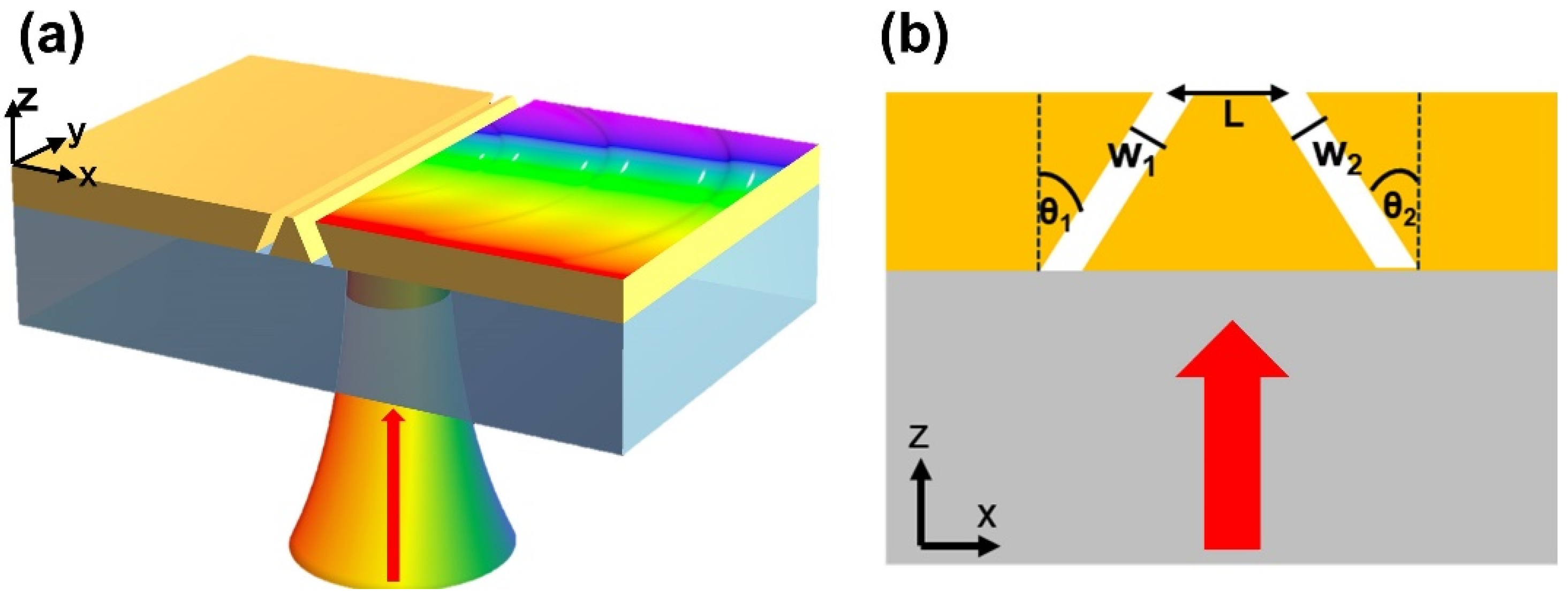
The schematic diagram of the broadband directional coupler is shown in Figure 1. A pair of nanoslits is obliquely perforated into a gold film deposited on a glass substrate. When a TM polarized light is incident on the structure from the glass side, each nanoslit acts as a nanoantenna to couple free space light to plasmonic modes propagating on the surface. The wavevector of the SPP field sustained at the gold/air interface can be expressed as
where λ is the wavelength of incident light and εm is the permittivity of gold dependent on λ. The thickness of gold film is 160 nm to block the incident light onto the gold/air interface. The directional coupling of SPPs by double-slit relies on the asymmetric excitation of plasmonic fields in each individual slit. The SPP field propagating along the ±x directions can be expressed as
where L is the distance between the slits and and (i = 1, 2) denote the coupling efficiency and phase of the SPP wave generated by each slit propagating along ±x axis. When the plasmonic field propagating in one direction is suppressed by destructive interference, whereas constructive interference occurs on the other side, the directional coupling of SPPs is realized. Assuming the plasmonic field is propagating along the positive x axis directionally, the coupling phase difference is expressed as

Figure 1.
(a) Schematic diagram of the broadband directional SPP coupler with a pair of oblique nanoslits etched on a gold film. The colored ripple at xy plane represents the plasmonic fields excited by different wavelength, which propagates directionally along positive x axis. (b) Cross sectional view of the structure along xz plane. The direction of the incident wave vector is indicated by the red arrows in (a,b).
Equations (4) and (5) can be satisfied at a specific wavelength by adjusting the structural parameters of each slit, and there are many studies on the directional coupling of SPPs by rectangular slit pairs [29,32,33]. In that case, the coupling phase of the plasmonic field propagating along the two sides of individual slit is identical (, ) and optimal directional coupling can be achieved with φ2 − φ1 = ksppL = π/2. In general, the coupling phase is dependent on the effective refractive index of the cavity mode inside the slit, and φ2 − φ1 barely changes with wavelength. While the wavevector of SPPs varies significantly with wavelength, this leads to a drift of phase difference as the incidence deviates from the central wavelength, weakening the destructive interference in Equation (3). Hence, the operating wavelength in previous research is always limited to a narrow band.
To compensate the additional propagating phase term ΔksppL as the wavelength changes, oblique nanoslits are employed in Figure 1. When incident light illuminates the gold film perpendicularly along the z-axis, oblique slits scatter light asymmetrically, exciting plasmonic fields on either side of the slit with different intensities and phases. The coupling phase exhibits a dependence on both the tilting angle of the slit and the incident wavelength, primarily due to the increased optical path length within the slit. This gives rise to varying coupling phase differences φ2–φ1 as the wavelength changes, which can compensate the additional propagating phase.
3. Numerical Results
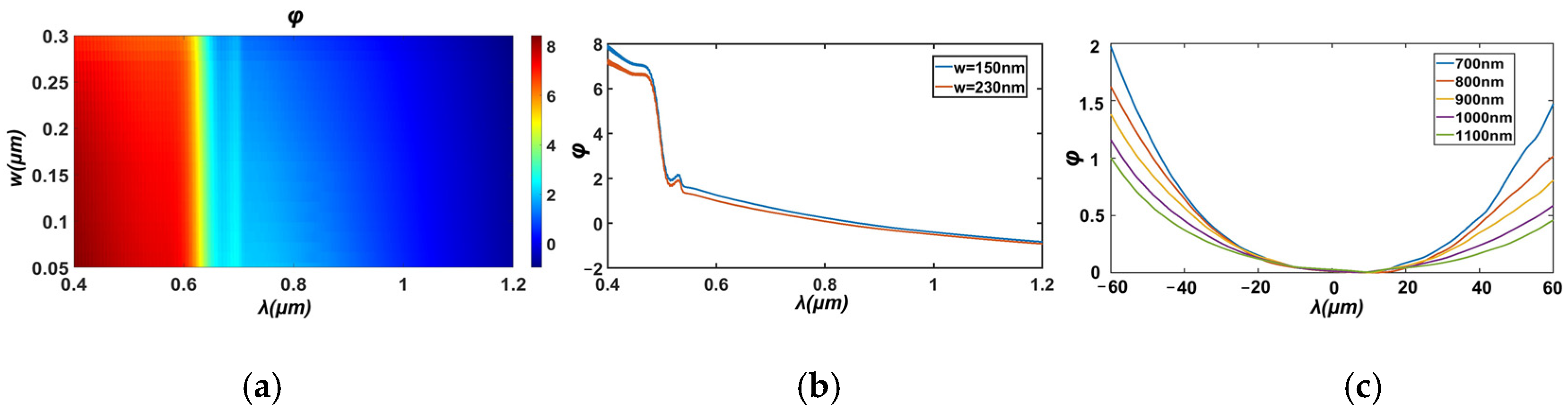
The interaction between incident wave and nanoslit is simulated using the two-dimensional finite-difference time-domain (FDTD) method in the commercial software (Lumerical 2023R1). The boundary conditions in the x and z directions are set as perfectly matched layers (PML) absorbing boundary conditions. To evaluate the coupling efficiency and phase, the nanoslit etched on the gold layer is illuminated at normal incidence by a linearly polarized plane wave underneath the sample. A point monitor is placed at the gold/air interface and 10 μm away from the right edge of the slit to measure the coupling efficiency and phase. A non-uniform mesh is used throughout the whole simulation domain and the minimum mesh size is 1 nm. The unit sizes and time steps ensure that the values of the electromagnetic fields and current densities in the spatial grid are converged and stable. Figure 2a illustrates the dependence of the coupling phase of individual rectangular slits on both slit width and incident wavelength. At a fixed wavelength, the coupling phase exhibits a slight dependence on slit width, enabling directional coupling of SPPs using a pair of asymmetric slits. In contrast, the coupling phase demonstrates a significant dependence on the incident wavelength, as illustrated in Figure 2b for two distinct slit widths of 150 nm and 230 nm. However, the phase difference in Figure 2b exhibits minimal variation with wavelength, particularly for wavelengths exceeding 500 nm, which corresponds to the typical plasmonic resonance regime for gold. Hence, the operating wavelength for directional coupling is limited in terms of the rectangular nanoslit pair. As the slit is tilted, the initial coupling phase is altered due to the resultant increase in optical path length, which depends on the incident wavelength. Figure 2c illustrates the coupling phase dependence on the slit tilt angle for different wavelengths. As can be observed in Figure 2c, the coupling phase exhibits an increase with both the tilt angle and the wavevector. This provides an additional degree of freedom for manipulating the plasmonic fields excited by the nanoslits. Specifically, the coupling phase difference between two distinct oblique slits increases with the wavevector, compensating for the additional propagating phase ΔksppL as the wavelength changes. The phase difference between the plasmonic fields for destructive interference is maintained at approximately π across a wide range of wavelengths, giving rise to broadband directional coupling of SPPs.

Figure 2.
(a) Plasmonic coupling phase dependence on incident wavelengths and slit width for rectangular slit. (b) Coupling phase of SPP varies on incident wavelength excited for slit widths of 150 nm and 230 nm, respectively. (c) Coupling phase of SPP varies on the tilt angle of the slit at a width of 150 nm for different wavelengths.
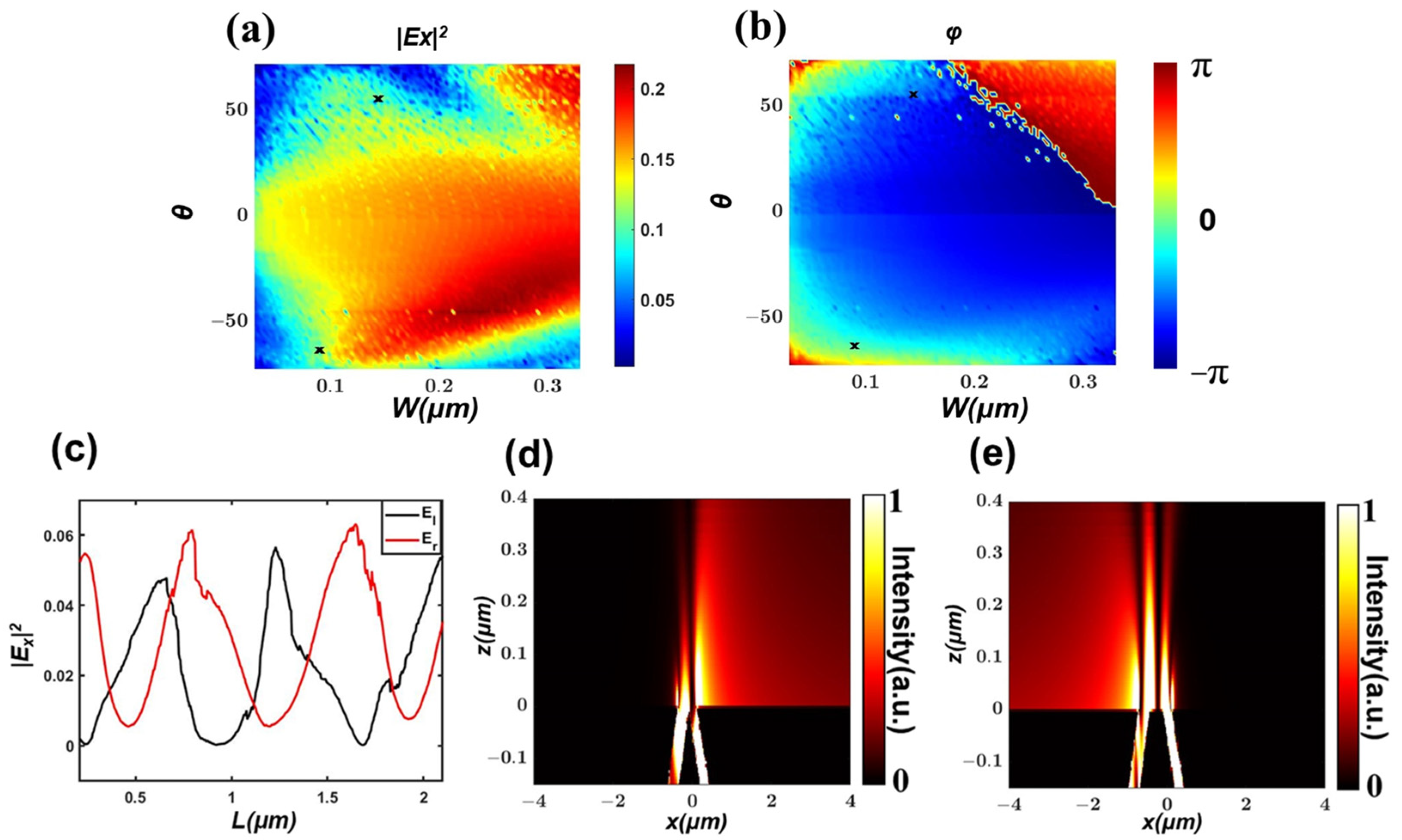
The dependence of the coupling efficiency η and phase φ on both slit width and tilt angle for individual slits are demonstrated in Figure 3a,b at a wavelength of 750 nm, respectively. As the tilt angle of the slit increases, the coupling efficiency shown in Figure 3a decreases, which is related to the dispersion relation of SPPs; meanwhile, the coupling phase in Figure 3b increases with the angle, consistent with the explanation provided in Figure 2. Guided by this pattern, a series of slit parameters that meet the conditions can be identified. Destructive interference of the plasmonic field occurs when the coupling phase difference between individual slits satisfies φ2 − φ1 = (N + 1/2)π. In addition, the coupling efficiency for each slit should be equal to optimize the directional excitation of SPPs. In order to achieve this, we select the widths and tilt angle of the slits as w1 = 90 nm, θ1 = −63° and w2 = 145 nm, θ2 = 56°, which give η1 ≈ η2~13%, φ2~φ1 ≈ π/2. The interference fields on each side exhibit oscillations as the slit spacing varies. Notably, the amplitude variations on each side of the double slit closely resemble sine functions with a distinct phase shift between them, as shown in Figure 3c. Plasmonic fields propagate directionally along the −x axis at an optimal distance of L = 230 nm. Conversely, at L = 520 nm, plasmonic fields propagate directionally along the x-axis. Figure 3d,e depicts the near-field distributions of the electric field under normal plane-wave illumination for L = 230 nm and L = 520 nm, respectively, demonstrating strong directionality in both cases. This nanoscale tilted slit can be fabricated using a focused ion beam (FIB) with tilted exposure or angled ion milling. Given the desired slit angle, the tilt angle of the FIB sample stage can be calculated to ensure the ion beam precisely mills the nanoslit at the intended angle.

Figure 3.
Dependence of (a) coupling efficiency η and (b) coupling phase φ of the SPPs on the slit width and tilt angle for a wavelength of 750 nm. The markers ‘×’ denote the geometric parameters of the asymmetric slits considered for directional coupling. (c) The amplitude variations on each side of the double slit. (d,e) Simulated near-field distribution of the electric field in the x–z plane for slit spacing of (d) L = 230 nm and (e) L = 520 nm.
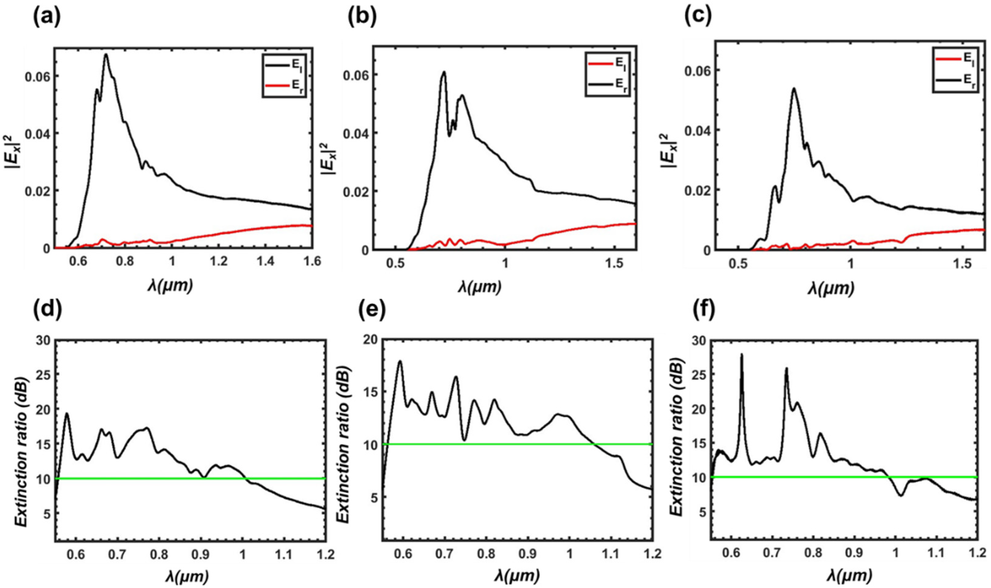
Oblique slits enable directional coupling of SPPs across a broad spectral range. Figure 4a illustrates the electric field intensities on both sides of the nanoantenna under broadband light source excitation ranging from 400 nm to 1600 nm for L = 230 nm, demonstrating a directional coupling in a broadband spectrum. To quantify the directional coupling performance, the extinction ratio is defined as the ratio of the intensities of SPPs propagating in opposite directions as
where Er and El denote x components of electric field along positive and negative x directions at z = 0 plane, respectively. The bandwidth of directional coupling is defined as the wavelength range within which the extinction ratio, as defined in Equation (6), exceeds 10. This extinction ratio threshold is considered sufficient for achieving efficient unidirectional SPP coupling in large-scale devices [15]. Figure 4b illustrates the simulated extinction ratio as a function of wavelength. Within the wavelength range of 550–950 nm, SPPs propagate directionally along the x axis, exhibiting a maximum extinction ratio of 30 dB. The near-field distribution of the electric field under broadband plane-wave illumination within the wavelength range of 550–950 nm is depicted in Figure 4c, confirming directional coupling across this broad spectral range. For comparison, the directional coupling performance for rectangular nanoslits is also simulated, as depicted in Figure 4d–f. In Figure 4, a notable difference in the directional coupling efficiency between the inclined slit and the rectangular slit can be observed. Under excitation by a broadband light source ranging from 400 nm to 1600 nm, there is a significant disparity in the electric field intensity on both sides of the inclined slit, which enables effective directional coupling transmission within the wavelength range of 550 nm to 950 nm. In contrast, for the rectangular slit, there is no significant difference in electric field intensity on either side when stimulated by the same light source. Figure 4c,f clearly illustrates the directional transmission capabilities of the inclined and rectangular slits.
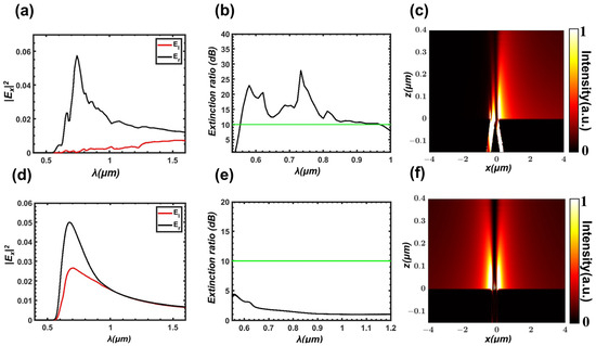
Figure 4.
(a–c) Directional coupling of SPPs for oblique nanoslits under broadband light source excitation. (a) The electric field intensity of SPPs propagating along the x (black solid line) and −x (red solid line). (b) Extinction ratio (black line) calculated from (a), with the green line indicating an extinction ratio of 10. (c) Near field distribution of the electric field under broadband light source excitation. (d–f) Directional coupling of SPPs for rectangular nanoslits under broadband light source excitation using the same slit width as in the oblique case. (d) The electric field intensity of SPPs propagating along both sides, (e) extinction ratio, and (f) near field distribution of the electric field.
The proposed structure demonstrates robust directional coupling performance even with deviations from the optimal slit parameters. To assess the impact of fabrication errors, we analyzed the effects of varying slit width, tilt angle, and slit spacing. As shown in Figure 5, the directional coupling behavior remains unaffected despite these parameter variations. While the coupling efficiency and extinction ratio exhibit slight changes, remaining within an acceptable range, the bandwidth maintains its similarity to that achieved with the optimal parameters. This indicates a good fabrication tolerance for the directional coupler.
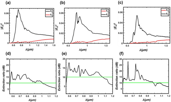
Figure 5.
The intensity and extinction ratio as the slit parameter changes. (a–c) The electric field intensity of SPPs propagating along the x (black solid line) and −x (red solid line) axis for (a) w1 = 100 nm, w2 = 155 nm with fixed tilt angle and slit spacing; (b) θ1 = −68°, θ2 = 61° with fixed slit width and spacing; (c) L = 250 nm with fixed slit width and tilt angle. (d–f) The corresponding extinction ratios (black lines) are calculated from (a–c), with the green lines indicating an extinction ratio of 10, where the bandwidth of the directional coupling is 450 nm, 480 nm, and 430 nm, respectively.
4. Conclusions
In conclusion, we propose a broadband directional coupler of SPPs by applying a pair of oblique nanoslits. We demonstrate that tilting the slit can significantly enhance the sensitivity of plasmonic coupling phase variation with respect to the wavelength of incident light, enabling more precise wavelength-dependent control over SPP propagation. By optimizing the width and tilting angle of each nanoslit, the ratio of SPP excitation in opposite directions exceeds 10 dB with a bandwidth exceeding 400 nm, spanning the visible and near-infrared spectral range. The results enable efficient and flexible control over light propagation at the nanoscale, paving the way for the development of novel devices with advanced functionalities, such as ultra-compact optical interconnects, biosensors, and nonlinear optical components.
Author Contributions
Conceptualization, X.L., J.Z. and Q.Z.; methodology, X.L.; software, C.C. and Q.W.; validation, C.C., Q.W. and X.L.; formal analysis, C.C. and Q.W.; investigation, C.C.; resources, X.L. and Q.Z.; data curation, C.C.; writing—original draft preparation, C.C.; writing—review and editing, X.L.; visualization, C.C.; supervision, X.L. and Q.Z.; project administration, X.L.; funding acquisition, X.L. and Q.Z.; All authors have read and agreed to the published version of the manuscript.
Funding
This work was supported by the National Natural Science Foundation of China (12434012, 12204309, 12304367); Shanghai Rising-Star Program (22YF1415200, 23YF1415800); and Shanghai Post-doctoral Excellence Program (2023533).
Institutional Review Board Statement
Not applicable.
Informed Consent Statement
Not applicable.
Data Availability Statement
The data presented in this study are available on request from the corresponding author.
Conflicts of Interest
The authors declare no conflicts of interest.
References
- Wang, H.; Zhang, Y.; He, Y.; Zhu, Q.; Sun, L.; Su, Y. Compact Silicon Waveguide Mode Converter Employing Dielectric Metasurface Structure. Adv. Opt. Mater. 2019, 7, 1801191. [Google Scholar]
- Karabchevsky, A.; Katiyi, A.; Ang, A.S.; Hazan, A. On-chip nanophotonics and future challenges. Nanophotonics 2020, 9, 3733–3753. [Google Scholar]
- Tonndorf, P.; Del Pozo-Zamudio, O.; Gruhler, N.; Kern, J.; Schmidt, R.; Dmitriev, A.I.; Bakhtinov, A.P.; Tartakovskii, A.I.; Pernice, W.; Michaelis de Vasconcellos, S.; et al. On-Chip Waveguide Coupling of a Layered Semiconductor Single-Photon Source. Nano Lett. 2017, 17, 5446–5451. [Google Scholar]
- Nair, R.V.; Vijaya, R. Photonic crystal sensors: An overview. Prog. Quantum Electron. 2010, 34, 89–134. [Google Scholar]
- Novotny, L.; van Hulst, N. Antennas for light. Nat. Photon. 2011, 5, 83–90. [Google Scholar]
- Mühlschlegel, P.; Eisler, H.-J.; Martin, O.J.F.; Hecht, B.; Pohl, D.W. Resonant Optical Antennas. Science 2005, 308, 1607–1609. [Google Scholar]
- Kosako, T.; Kadoya, Y.; Hofmann, H.F. Directional control of light by a nano-optical Yagi–Uda antenna. Nat. Photon. 2010, 4, 312–315. [Google Scholar]
- Guo, R.; Decker, M.; Setzpfandt, F.; Gai, X.; Choi, D.-Y.; Kiselev, R.; Chipouline, A.; Staude, I.; Pertsch, T.; Neshev, D.N.; et al. High–bit rate ultra-compact light routing with mode-selective on-chip nanoantennas. Sci. Adv. 2017, 3, e1700007. [Google Scholar]
- Kim, I.; Jang, J.; Kim, G.; Lee, J.; Badloe, T.; Mun, J.; Rho, J. Pixelated bifunctional metasurface-driven dynamic vectorial holographic color prints for photonic security platform. Nat. Commun. 2021, 12, 3614. [Google Scholar]
- Koenderink, A.F.; Alù, A.; Polman, A. Nanophotonics: Shrinkinglight-based technology. Science 2015, 348, 516–521. [Google Scholar]
- Maier, S.A.; Kik, P.G.; Atwater, H.A.; Meltzer, S.; Harel, E.; Koel, B.E.; Requicha, A.A.G. Local detection of electromagnetic energy transport below the diffraction limit in metal nanoparticle plasmon waveguides. Nat. Mater. 2003, 2, 229–232. [Google Scholar] [CrossRef] [PubMed]
- Bozhevolnyi, S.I.; Volkov, V.S.; Devaux, E.; Laluet, J.-Y.; Ebbesen, T.W. Channel plasmon subwavelength waveguide components including interferometers and ring resonators. Nature 2006, 440, 508–511. [Google Scholar] [CrossRef] [PubMed]
- Oulton, R.F.; Sorger, V.J.; Zentgraf, T.; Ma, R.-M.; Gladden, C.; Dai, L.; Bartal, G.; Zhang, X.J. Plasmon lasers at deep subwavelength scale. Nature 2009, 461, 629–632. [Google Scholar] [CrossRef] [PubMed]
- Yang, A.; Hoang, T.B.; Dridi, M.; Deeb, C.; Mikkelsen, M.H.; Schatz, G.C.; Odom, T.W. Real-time tunable lasing from plasmonic nanocavity arrays. Nat. Commun. 2015, 6, 6939. [Google Scholar] [CrossRef]
- Baron, A.; Devaux, E.; Rodier, J.C.; Hugonin, J.P.; Rousseau, E.; Genet, C.; Ebbesen, T.W.; Lalanne, P. Compact Antenna for Efficient and Unidirectional Launching and Decoupling of Surface Plasmons. Nano Lett. 2011, 11, 4207–4212. [Google Scholar] [CrossRef]
- Knight, M.W.; Sobhani, H.; Nordlander, P.; Halas, N.J. Photodetection with Active Optical Antennas. Science 2011, 332, 702–704. [Google Scholar] [CrossRef]
- Melikyan, A.; Alloatti, L.; Muslija, A.; Hillerkuss, D.; Schindler, P.C.; Li, J.; Palmer, R.; Korn, D.; Muehlbrandt, S.; Van Thourhout, D.; et al. High-speed plasmonic phase modulators. Nat. Photon. 2014, 8, 229–233. [Google Scholar] [CrossRef]
- Ayata, M.; Fedoryshyn, Y.; Heni, W.; Baeuerle, B.; Josten, A.; Zahner, M.; Koch, U.; Salamin, Y.; Hoessbacher, C.; Haffner, C.; et al. High-speed plasmonic modulator in a single metal layer. Science 2017, 358, 630–632. [Google Scholar] [CrossRef]
- Huang, H.; Overvig, A.C.; Xu, Y.; Malek, S.C.; Tsai, C.-C.; Alù, A.; Yu, N. Leaky-wave metasurfaces for integrated photonics. Nat. Nanotechnol. 2023, 18, 580–588. [Google Scholar] [CrossRef]
- Kabashin, A.V.; Evans, P.; Pastkovsky, S.; Hendren, W.; Wurtz, G.A.; Atkinson, R.; Pollard, R.; Podolskiy, V.A.; Zayats, A.V. Plasmonic nanorod metamaterials for biosensing. Nat. Mater. 2009, 8, 867–871. [Google Scholar] [CrossRef]
- Gao, Y.; Gan, Q.; Xin, Z.; Cheng, X.; Bartoli, F.J. Plasmonic Mach–Zehnder Interferometer for Ultrasensitive On-Chip Biosensing. ACS Nano 2011, 5, 9836–9844. [Google Scholar]
- Liu, Z.; Steele, J.M.; Srituravanich, W.; Pikus, Y.; Sun, C.; Zhang, X. Focusing Surface Plasmons with a Plasmonic Lens. Nano Lett. 2005, 5, 1726–1729. [Google Scholar] [CrossRef]
- Chen, W.; Abeysinghe, D.C.; Nelson, R.L.; Zhan, Q. Plasmonic Lens Made of Multiple Concentric Metallic Rings under Radially Polarized Illumination. Nano Lett. 2009, 9, 4320–4325. [Google Scholar] [CrossRef] [PubMed]
- Zhao, C.; Zhang, J. Plasmonic demultiplexer and guiding. ACS Nano 2010, 4, 6433–6438. [Google Scholar] [CrossRef]
- Li, X.; Tan, Q.; Bai, B.; Jin, G. Experimental demonstration of tunable directional excitation of surface plasmon polaritons with a subwavelength metallic double slit. Appl. Phys. Lett. 2011, 98, 251109. [Google Scholar]
- Radko, I.P.; Bozhevolnyi, S.I.; Brucoli, G.; Martin-Moreno, L.; Garcia-Vidal, F.J.; Boltasseva, A. Efficient unidirectional ridge excitation of surface plasmons. Opt. Express 2009, 17, 7228–7232. [Google Scholar] [CrossRef] [PubMed]
- López-Tejeira, F.; Rodrigo, S.G.; Martín-Moreno, L.; García-Vidal, F.J.; Devaux, E.; Ebbesen, T.W.; Krenn, J.R.; Radko, I.P.; Bozhevolnyi, S.I.; González, M.U.; et al. Efficient unidirectional nanoslit couplers for surface plasmons. Nat. Phys. 2007, 3, 324–328. [Google Scholar]
- Liu, T.; Shen, Y.; Shin, W.; Zhu, Q.; Fan, S.; Jin, C. Dislocated double-layer metal gratings: An efficient unidirectional coupler. Nano Lett. 2014, 14, 3848–3854. [Google Scholar]
- Bai, B.; Meng, X.; Laukkanen, J.; Sfez, T.; Yu, L.; Nakagawa, W.; Herzig, H.P.; Li, L.; Turunen, J. Asymmetrical excitation of surface plasmon polaritons on blazed gratings at normal incidence. Phys. Rev. B Condens. Matter 2009, 80, 1132–1136. [Google Scholar]
- Chen, J.; Li, Z.; Yue, S.; Gong, Q. Efficient unidirectional generation of surface plasmon polaritons with asymmetric single-nanoslit. Appl. Phys. Lett. 2010, 97, 041113. [Google Scholar] [CrossRef]
- Yao, W.; Liu, S.; Liao, H.; Li, Z.; Sun, C.; Chen, J.; Gong, Q. Efficient directional excitation of surface plasmons by a single-element nanoantenna. Nano Lett. 2015, 15, 3115. [Google Scholar] [PubMed]
- Chen, P.; Chen, C.; Qin, S.; Xi, J.; Huang, W.; Shi, F.; Li, K.; Liang, L.; Shi, J. Efficient planar plasmonic directional launching of linearly polarized light in a catenary metasurface. Phys. Chem. Chem. Phys. 2020, 22, 27554–27559. [Google Scholar] [PubMed]
- Yang, J.; Xiao, X.; Hu, C.; Zhang, W.; Zhou, S.; Zhang, J. Broadband surface plasmon polariton directional coupling via asymmetric optical slot nanoantenna pair. Nano Lett. 2014, 14, 704. [Google Scholar]
- Liu, J.S.; Pala, R.A.; Afshinmanesh, F.; Cai, W.; Brongersma, M.L. A submicron plasmonic dichroic splitter. Nat. Commun. 2011, 2, 525. [Google Scholar] [CrossRef] [PubMed]
- Liao, H.; Li, Z.; Chen, J.; Zhang, X.; Yue, S.; Gong, Q. A submicron broadband surface-plasmon-polariton unidirectional coupler. Sci. Rep. 2013, 3, 1918. [Google Scholar] [CrossRef]
- Xu, G.; Overvig, A.; Kasahara, Y.; Martini, E.; Maci, S.; Alù, A. Arbitrary aperture synthesis with nonlocal leaky-wave metasurface antennas. Nat. Commun. 2023, 14, 4380. [Google Scholar]
- Gupta, N.; Dhawan, A. Harnessing surface plasmon polaritons from nanogroove plasmonic lenses to enhance the EM fields around plasmonic nanoantennas. J. Opt. Soc. Am. B 2024, 41, 2247–2258. [Google Scholar]

Disclaimer/Publisher’s Note: The statements, opinions and data contained in all publications are solely those of the individual author(s) and contributor(s) and not of MDPI and/or the editor(s). MDPI and/or the editor(s) disclaim responsibility for any injury to people or property resulting from any ideas, methods, instructions or products referred to in the content. |
© 2025 by the authors. Licensee MDPI, Basel, Switzerland. This article is an open access article distributed under the terms and conditions of the Creative Commons Attribution (CC BY) license (https://creativecommons.org/licenses/by/4.0/).