Abstract
As the popularity of Internet of Things (IoT) increases, there is a considerable demand for the improvement of physical security, owing to the increase in edge devices. However, fabrication and measurement techniques used by attackers are also improving continuously, and hence, it is becoming increasingly difficult to ensure the security of each device using conventional approaches. To counter variable attacks in this context, the concept of nano-photonic metrics has been proposed, which is based on a functional collaboration between existing physical security and near-field optical techniques. In this approach, the optical signals obtained from optical near-field interactions, which are induced between the target with nano-scale structures and the tip of the scanning probe as the reader, are defined as the unique features of each device to be authenticated. When attackers attempt spoofing, they must fabricate not only clones of original nano-scale structures but also the scanning probe; otherwise, they cannot impersonate regular users. Moreover, the estimation of the nano-scale structures of the target and the characteristics of the probe is typically a complex, inverse problem. Therefore, a novel authentication is expected to be performed. In this paper, we report the results of the quantitative evaluations of the performance from the viewpoint of physical security and the experimental verification of the practicality of the proposed approach.
1. Introduction
With the increasing popularity of Internet of Things (IoT), the number of edge devices has been continuously increasing as gateways between the Internet and the real world. Simultaneously, there are social requirements to improve the performance of physical security systems, which can definitely exclude widespread access to the Internet via disapproved edge devices and their electrical components. Thus, artifact metrics [1] are among the most promising concepts for addressing such requirements. A manufacturer tries to give unique, novel, and physical features to individual devices and components such that they are difficult to accurately counterfeit, and an attacker seeks a method to counterfeit such features [2]. Physical features include electromagnetic [3,4], mechanical, and optical properties [5,6]. Simultaneously, corresponding measurement technologies must be developed to read out each physical feature. In recent years, advanced fabrication and measurement technologies have become increasingly common. It is desirable to further popularize artifact metrics. However, at the same time, this means that disapproved artifacts can also be fabricated by utilizing such technologies. Therefore, it is difficult to ensure the security of edge devices using conventional approaches, which depend on the technical difficulty of counterfeiting.
To this end, we recently proposed the concept of nano-photonic metrics [7], which is based on the functional collaboration between conventional artifact metrics and near-field optical techniques [8]. The optical nearfields behave as a virtual cloud of photons that are constantly localized around nanostructures illuminated by the incident light. As the virtual cloud of photons is localized in a region close to the electrons in the material, they can effectively interact with the materials in a unique manner [8]. In nano-photonic metrics, the physical features of an artifact with nanostructures are experimentally determined using near-field optical microscopy (NOM). NOM is an advanced method for obtaining two-dimensional images of spatially distributed optical nearfields based on high-resolution interactions between the probe and the nanostructures of the target [9]. The optical response, derived from the optical near-field interactions generated between the tip of the probe and the nanostructures on the surface of the artifact, is utilized as individual information that is unique to each artifact. Since this response varies greatly depending not only on the nanostructures but also on the specifications of the probe, such as the size, material, and physical behavior, it is expected that readout optical response will include sufficient characteristics of both the nanostructure and the probe to be identified. Moreover, in principle, it is difficult to duplicate the probe or nanostructures from stalled optical responses. The performance of nano-photonic metrics is affected not only by the technological difficulty in duplicating nanostructures but also by the fundamental improbability of estimating the characteristic behavior of optical near-field interactions [8] between the probe and the nanostructures. In general, the use of NOM entails a scanning process, which is not necessarily required in security applications. However, from a previous study [7], it is known that a clear, signal difference can be obtained between different nanostructures using a non-scanning readout process.
In this paper, we report quantitative evaluations of the performance of nano-photonic metrics. The performance is discussed based on the values of the false match rate (FMR) and false non-match rate (FNMR), which are quantitative indices that reveal the individuality and readout stability of the security system, respectively, from the results of multiple readouts using non-scanning NOM. Furthermore, the origin of the performance is discussed by analyzing the NOM results, and the corresponding dynamics of the optical near-field interactions during the readout process is clarified.
2. Nano-Photonic Metrics
The basic architecture of the nano-photonic metric system is illustrated schematically in Figure 1. Here, we anticipate the utilization of the non-scanning NOM for the identification of nano-photonic features of the artifacts. In the nano-scale field, the probe continuously fluctuates to maintain its mean distance from the surface of the artifact. During these fluctuations, various scales of interaction between the probe and artifact are sequentially induced based on the size resonance effect of the optical near-field interaction [10]. This means that by fluctuating on a fixed readout point on the target, the probe induces interactions between not only the structure underneath but also the surrounding structures of the artifact. Hence, readout signals during fluctuations are expected to include sufficient information regarding the structural distribution of the artifact without any scanning process.
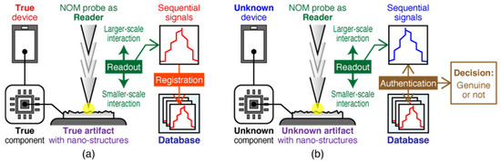
Figure 1.
Fundamental system architecture of nano-photonic metrics based on non-scanning NOM consists of (a) initial registration of true target and (b) authentication of an unknown target.
The first registration process must be executed, as shown in Figure 1a. In this process, a single stroke of the periodically oscillating tip from the nearest to the farthest distance between the surfaces of the artifact was defined as a single readout. An appropriate readout signal with true artifacts is registered in the database, which is used as the template for the following authentication of an unknown artifact. During the authentication process, as shown in Figure 1b, we read out the signal output of the NOM from an unknown artifact to be authenticated by a procedure similar to the registration process to determine whether the artifact is genuine. The deciding factor is the score of similarity, the Pearson correlation coefficient [11], between the observed and registered signals.
3. Experimental Demonstration
To verify the performance of nano-photonic metrics, a non-scanning NOM with a SiO2 probe and substrate with Al nanorods were used as a reader and an artifact, respectively, as in our previous study [7]. A schematic diagram of the dynamics during the readout process using a non-scanning NOM is shown in Figure 2.
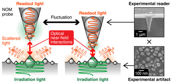
Figure 2.
Schematical diagram of dynamics during readout process with fluctuation by non-scanning NOM.
The probe was fabricated using a multistep HF etching process [12]. The shape of the tip can be arbitrarily varied by controlling various etching parameters, such as the composition of the HF solutions and the etching times. In our experiment, the radius of the curvature of the probe tip was set to less than 20 nm, and the tip was covered with a 50nm-thick Au layer formed by sputtering. A resonance oscillator with an oscillating frequency of 32 kHz was attached to the probe to monitor the molecular interaction, which is induced between the probe and the surface of the artifact during the readout process. This was done to control the shear force of the probe on the target to maintain a constant distance between them. Specifically, if the oscillating frequency increases, owing to the contribution of the molecular interaction, it can be assumed that the distance between the probe and the target decreases. In this case, the shear force must be decreased by reducing the applied voltage to the piezo actuator, which was set to the sample stage. In contrast, if the oscillating frequency decreases, the shear force must be increased by applying a higher voltage to the piezo actuator. Therefore, the probe position typically oscillates vertically. In our experiment, the mean distance between the probe and the artifact was set to be less than 50 nm.
The nanorods were grown on a Si substrate using the glancing angle deposition (GLAD) method [13]. Based on the size-resonance effect of probe–target interaction [10], for the induction of sufficient intensity of interactions, the size of the artifact on the target is preferred to reveal similar scales with the probe tip. Here, we prepared two types of artifacts: artifact 1 and artifact 2, which consisted of nanorods of various diameters, with mean diameters of 30 and 70 nm, respectively. A laser with a wavelength of 532 nm was used to induce optical near-field interactions, corresponding molecular interactions, and optical responses. Signals due to the optical responses were detected using a photomultiplier R-3896, manufactured by Hamamatsu Photonics, Japan, and read out as electrical signals. In nano-photonic metrics, the signals are utilized for the authentication of artifacts. SEM images of the tip of the probe and the surface of the nanorods are shown in the insets of Figure 2 as the experimental reader and artifact, respectively.
Figure 3a shows an example of the sequential readout results of the output signals due to optical response. As shown with the dashed line in Figure 3b, a time of less than 600 ms is required for a single readout in our experiment. Here, Figure 3b is the overlap of the results of two signals, which are readouts from individual Al nanorod samples. As shown in the figure, clear differences were obtained between the two, and nano-photonic metrics is expected to clearly determine whether a target artifact is genuine or not. In addition, an important matter is that injected voltage signals, which are simultaneously read out with optical signals by a non-scanning NOM, as shown in Figure 3c, do not reveal such variations. This is the reason for which optical signals are utilized for authentication in nano-photonic metrics.
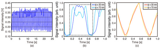
Figure 3.
(a) Sequential readout signal of non-scanning NOM due to optical response via optical near-field interactions. A comparison of results of (b) optical signals and (c) injected voltage signals against to two individual Al nanorod samples.
To quantitatively evaluate the security performance of the proposed system as an authentication system, the correlation coefficient between readout optical signals was calculated [14]. If an optical signal, denoted by , passes through the normalization of the amplitude and the time length, we calculated the correlations between the device under study and the template stored in the system, denoted , based on the Pearson correlation coefficient
where and are the average values of and , respectively. Based on , FMR and FNMR were evaluated as indicators of individuality and measurement stability, respectively. To calculate the FMR, if the similarity value given by Equation (1) was greater than a given threshold, the two signals were presumed to be the same, which is false. For the evaluation of the FNMR, if the similarity between two readouts from the same sample was smaller than a given threshold, the two signals were considered to be readout from different samples, which is false. In our experiment, we read more than 70 times at 20 points using two individual Al nanorod samples.
Figure 4 shows one of the calculated results of the FNMR and FMR curves, which was obtained by the appropriate selection of a registered signal. The solid and dashed lines represent the experimental results and their polynomial approximations, respectively. Generally, the equal error rate (EER) [15], which is defined as the crossed point of the FNMR and FMR curves, is often defined for quantitative evaluation, and if it is less than 10−5, it can be said to be sufficiently secure for practical use. Since there were only a few samples in our experiment, both solid lines reached a 10−1 error rate. However, if we evaluate the corresponding approximations using dashed lines, the EER is expected to be sufficiently low. As a result, it can be concluded that nano-photonic metrics display sufficient performance for practical use in the current information society.
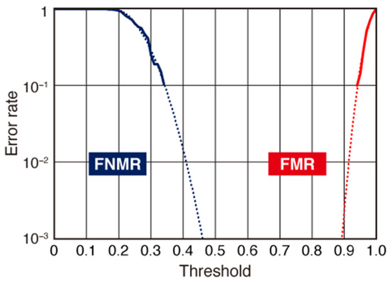
Figure 4.
Calculated results (solid lines) and approximated results (dashed lines) of FMR/FNMR.
4. Discussion
The performance of nano-photonic metrics can be discussed in terms of the characteristic behavior of optical near-field interactions during the readout process. In particular, in the case of the general scanning-use of NOM, only statistical results are obtained as two-dimensional images. However, in the case of our non-scanning use, sequential dynamics during fluctuations can be traced as readout signals, owing to the optical response and shear force of the probe. Here, we discuss the origin of the above dynamics by analyzing the readout signals.
NOM reads out signals using the optical response via fiber propagation of scattered light and the signal due to shear force of the probe by monitoring the amount of injection voltage to the piezo actuator. The piezo actuator, which is controlled by the probe, can maintain a constant distance between the artifacts. These were synchronized. Figure 5a shows an example of an overlapped signal. Unlike the optical signal, the shear force shows a simple fluctuation. Here, a decrease in the signal intensity corresponds with a decrease in the injection voltage to the piezoelectric actuator, and the probe is distanced from the artifact. An increase in the signal intensity induces the probe to approach the artifact. However, the fluctuation of the optical signal did not follow the fluctuation in shear force. In other words, the frequency and phase of the two are not similar. In particular, in step 4 of Figure 5a, the optical signal shows a peak in intensity despite the probe being at the farthest position from the artifact. This matter conflicts with the conventional model of the probe dynamics of NOM, and the construction of another model is needed. A schematic of the probe dynamics based on the experimental results is shown in Figure 5b.
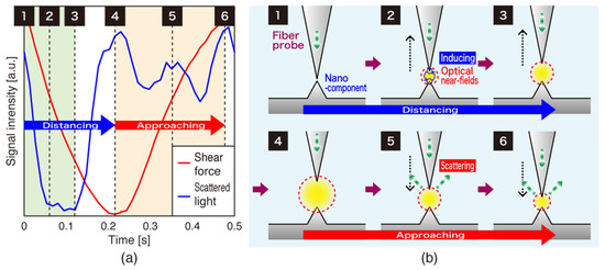
Figure 5.
(a) Experimentally obtained corresponding signal intensities. (b) Schematic of inducing and scattering of optical near-fields during a single cycle of nano-scale fluctuation of the probe.
Figure 5b starts from step 1, which corresponds to the situation after all optical energy due to optical near-fields is emitted. Irradiated light is continuously injected into the nano-space via the probe, and the capacitance of the optical near-fields is continuously increased according to the distance of the probe from the artifact, as in steps 2 to 3. Then, after the capacitance reaches the maximum value, the probe begins approaching the artifact from steps 4 to 6. During the steps, the capacitance becomes increasingly smaller, so that excess energy is continuously emitted as scattered light to the macro-space.
Here, as shown in Figure 5a, the amount of scattered light exhibits another fluctuation during the approach to the probe. We are now discussing how the size resonance effect of optical near-field interactions [10] affects this behavior. For example, from the comparison in Figure 3b, Al nanorod samples with a mean diameter of 70 nm exhibit a larger fluctuation width than those with 30 nm. This matter can be discussed as the former sample includes much variation in the diameter of nanorods than the latter, so various scales of optical near-field interactions are induced during the approaching process; as a result, the former reveals the clear modulation of the capacitance and corresponding optical signals.
5. Conclusions
With the goal of verifying the validity and effectiveness of nano-photonic metrics, we experimentally demonstrated their concept and their adequate performance for practical use. Specifically, its individuality and readout stability were quantitatively ensured by FMR, FNMR, and EER. In future studies, many more readout signals are needed to further calculate FMR/FNMR and indicate a more reliable EER instead of using approximation curves. Furthermore, the clone match rate (CMR) can be discussed. However, to discuss CMR, not only clones of artifacts, but also clones of probes must be prepared, and this is the fundamental reason that nano-photonic metrics are robust to clone attacks by attackers.
We introduced an original model of optical near-field interactions during the fluctuation of the NOM probe and explained the difference between the behaviors of the optical responses and the shear forces of the probe. In the future, we plan to investigate the characteristics of nano-photonic responses based on the model and intend to design nanostructures that emphasize these characteristics. These aspects, which were realized by exploiting nano-metrically fluctuating signals due to optical near-field interactions, are expected to be a conceptual breakthrough, not only for security applications but also for various research fields based on nano-photonics and nano-optics.
Author Contributions
Conceptualization, N.T.; methodology, N.T.; software, T.O. and S.-i.S.; validation, T.O. and S.-i.S.; formal analysis, T.O.; investigation, S.-i.S.; resources, N.T.; data curation, T.O. and S.-i.S.; writing—original draft preparation, T.O.; writing—review and editing, N.T.; visualization, N.T.; supervision, N.T.; project administration, N.T.; funding acquisition, N.T. All authors have read and agreed to the published version of the manuscript.
Funding
This research was funded by JSPS KAKENHI, grant number 17K14125.
Institutional Review Board Statement
Not applicable.
Informed Consent Statement
Not applicable.
Data Availability Statement
Data available in a publicly accessible repository.
Acknowledgments
Special thanks are due to Tadashi Kawazoe, NICHIA, for important the discussion on capacitance model of optical near-fields during the readout process of NOM.
Conflicts of Interest
The authors declare no conflict of interest.
References
- Matsumoto, H.; Matsumoto, T. Clone Match Rate Evaluation for an Artifact-metric System. IPSJ J. 2003, 44, 1991–2001. [Google Scholar]
- Van Renesse, R.L. Optical Document Security; Artech: Morristown, NJ, USA, 1994. [Google Scholar]
- Lim, D.; Lee, W.J.; Gassend, B.; Suh, G.E.; Van Dijk, M.; Devadas, S. Extracting Secret Keys from Integrated Circuits. IEEE Trans. Very Large Scale Integr. VLSI Syst. 2005, 13, 1200–1205. [Google Scholar]
- DeJean, G.; Darko, K. RF-DNA: Radio-frequency certificates of authenticity. In Proceedings of the Cryptographic Hardware and Embedded Systems—CHES 2007, 9th International Workshop, Vienna, Austria, 10–13 September 2007; Springer: Heidelberg, Germany, 2007; Volume 4727, pp. 346–363. [Google Scholar]
- Buchanan, J.D.; Cowburn, R.P.; Jausovec, A.V.; Petit, D.; Seem, P.; Xiong, G.; Bryan, M.T. Forgery: Fingerprinting documents and packaging. Nature 2005, 436, 475. [Google Scholar] [CrossRef]
- Yamakoshi, M.; Tanaka, J.; Furuie, M.; Hirabayashi, M.; Matsumoto, T. Individuality evaluation for paper based artifact-metrics using transmitted light image. Proc. SPIE 2008, 6819, 188–197. [Google Scholar] [CrossRef][Green Version]
- Tate, N.; Naruse, M.; Matsumoto, T.; Hoga, M.; Ohyagi, Y.; Nishio, S.; Nomura, W.; Ohtsu, M. Non-scanning optical near-field microscopy for nanophotonic security. Appl. Phys. A 2015, 121, 1383–1387. [Google Scholar] [CrossRef]
- Ohtsu, M. Dressed Photons—Concepts of Light-Matter Fusion Technology; Springer: Berlin, Germany, 2013. [Google Scholar]
- Hecht, B.; Sick, B.; Wild, U.P.; Deckert, V.; Zenobi, R.; Martin, O.J.F.; Pohl, D.W. Scanning near-field optical microscopy with aperture probes: Fundamentals and applications. J. Chem. Phys. 2000, 112, 7761–7774. [Google Scholar] [CrossRef]
- Sangu, S.; Kobayashi, K.; Ohtsu, M. Optical near fields as photon-matter interacting systems. J. Microsc. 2001, 202, 279–285. [Google Scholar] [PubMed]
- Kvalseth, T.O. Cautionary note about R2. Am. Stat. 1985, 39, 279–285. [Google Scholar]
- Mononobe, S. Fabrication of a double-tapered probe with enhanced aspect ratio for near-field scanning optical microscopy. Appl. Phys. A 2015, 121, 1365–1368. [Google Scholar] [CrossRef]
- Pihosh, Y.; Turkevych, I.; Ye, J.; Goto, M.; Kasahara, A.; Kondo, M.; Tosa, M. Physical and photocatalytic properties of TiO2 nanostructures fabricated by means of glancing angle deposition. ECS Trans. 2009, 16, 49–58. [Google Scholar] [CrossRef]
- Ohteki, T.; Mikami, Y.; Tate, N.; Oki, Y. Security performance of nano opt metric system based on near field optical interaction. In Proceedings of the 9th Korea-Japan Workshop on Digital Holography and Information Photonics, Gwangju, Korea, 18–20 November 2019. [Google Scholar]
- Duda, R.O.; Hart, P.E.; Stork, G. Pattern Classification, 2nd ed.; Wiley: New York, NY, USA, 2000. [Google Scholar]


Publisher’s Note: MDPI stays neutral with regard to jurisdictional claims in published maps and institutional affiliations. |
© 2022 by the authors. Licensee MDPI, Basel, Switzerland. This article is an open access article distributed under the terms and conditions of the Creative Commons Attribution (CC BY) license (https://creativecommons.org/licenses/by/4.0/).