
Growth of KNbO3 Single Crystals by the Flux Method Using KBO2 as a Flux
 , , , , , , and
Abstract
:1. Introduction
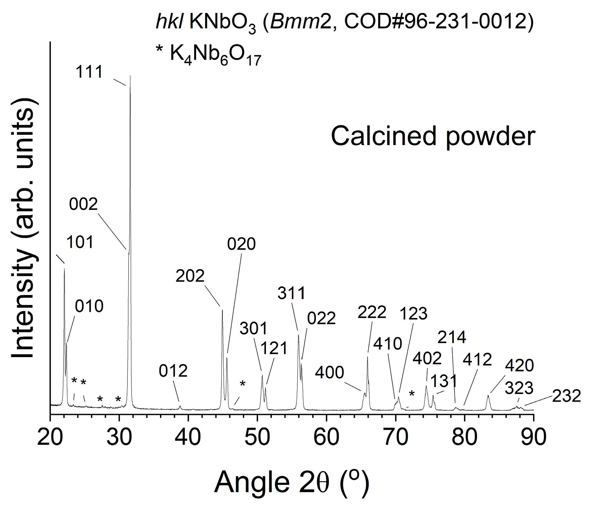
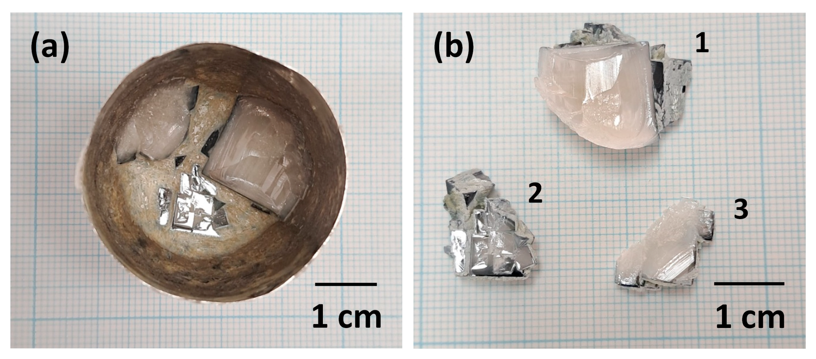
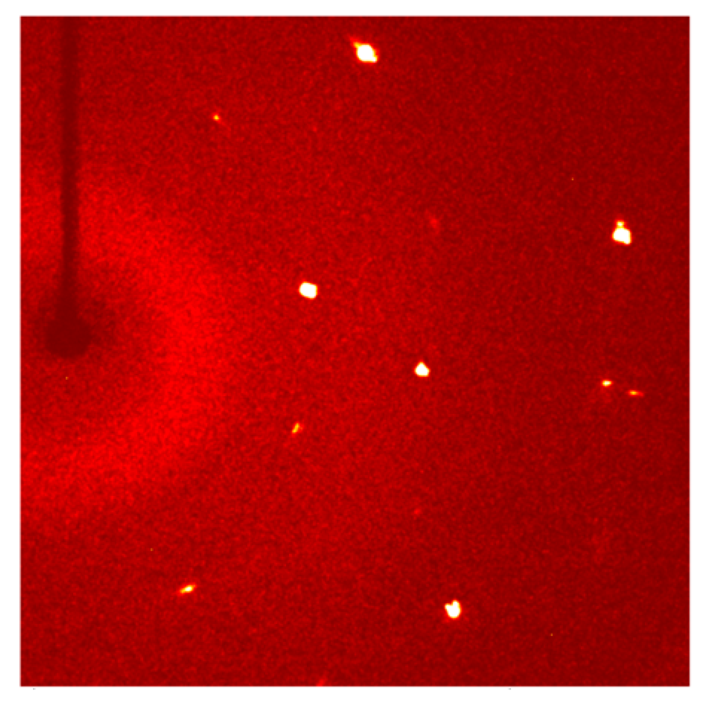
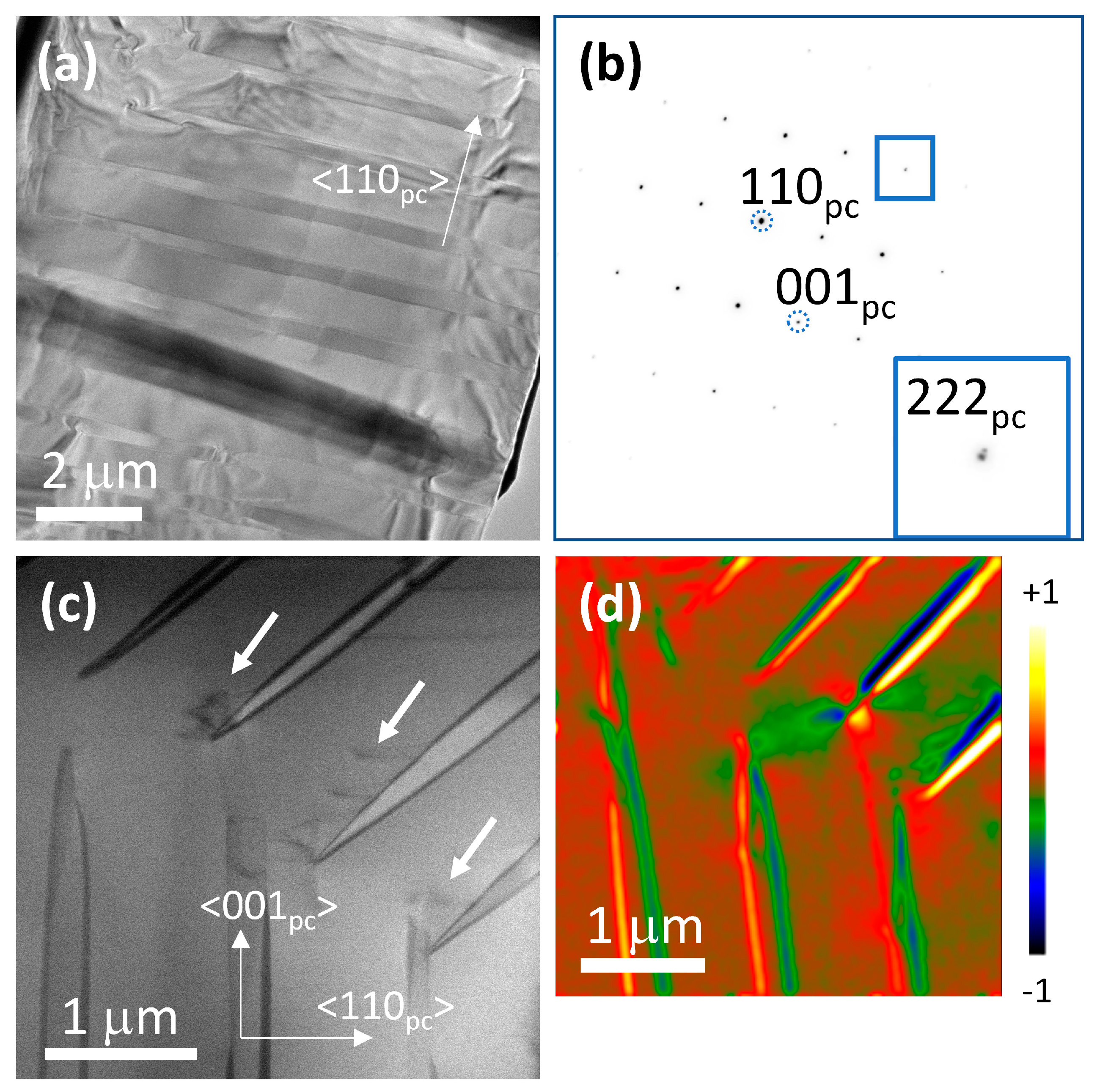
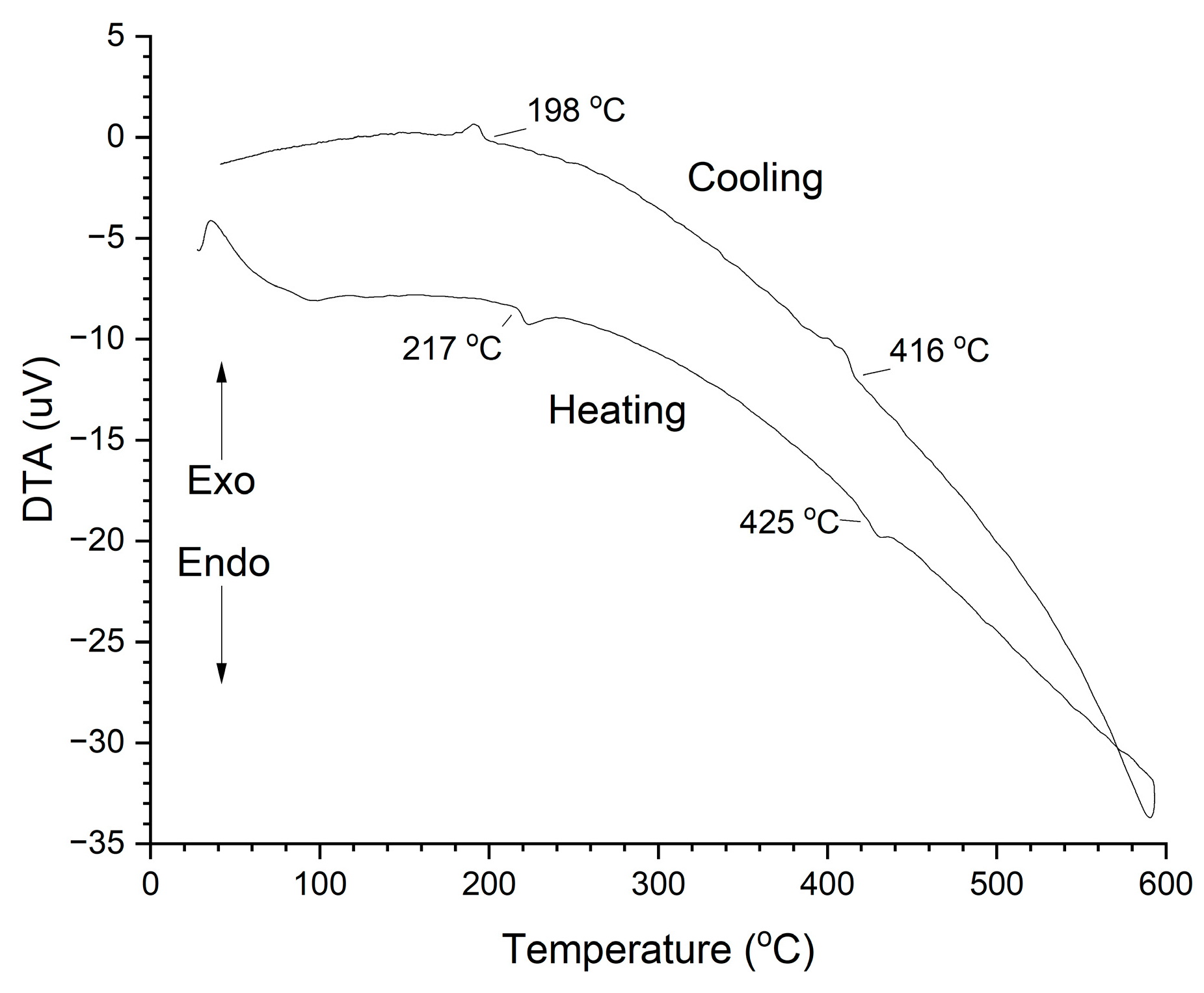
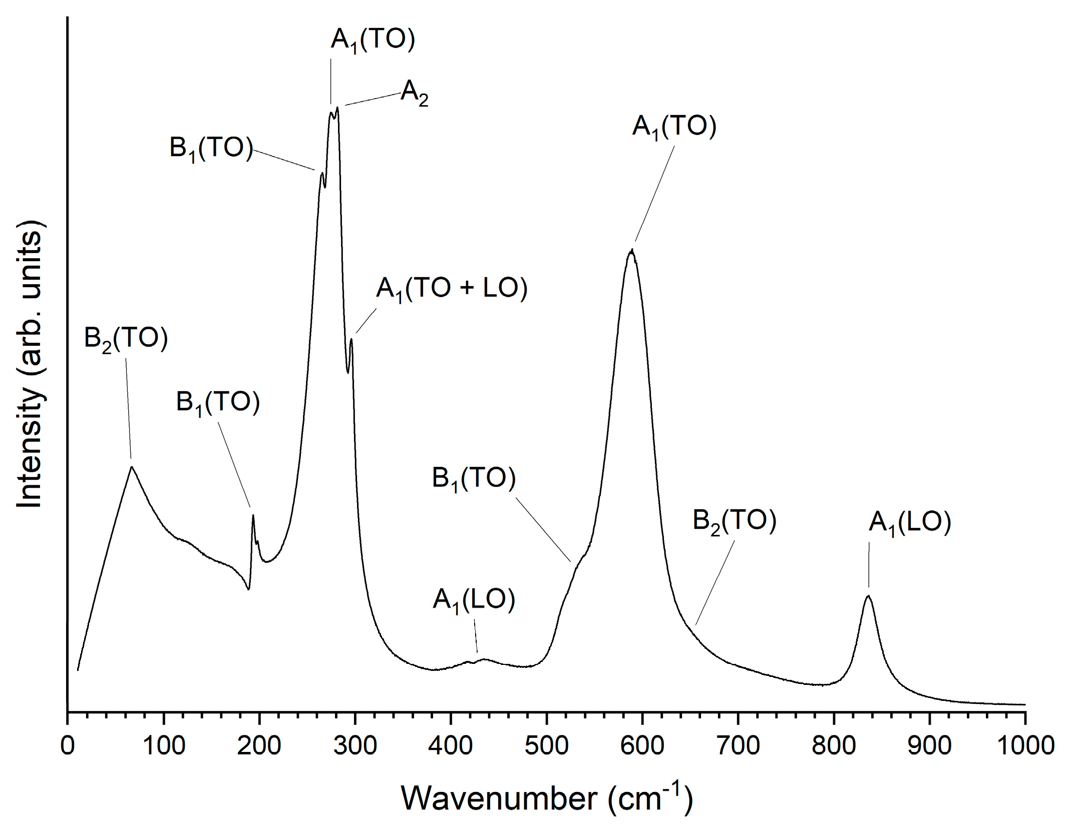
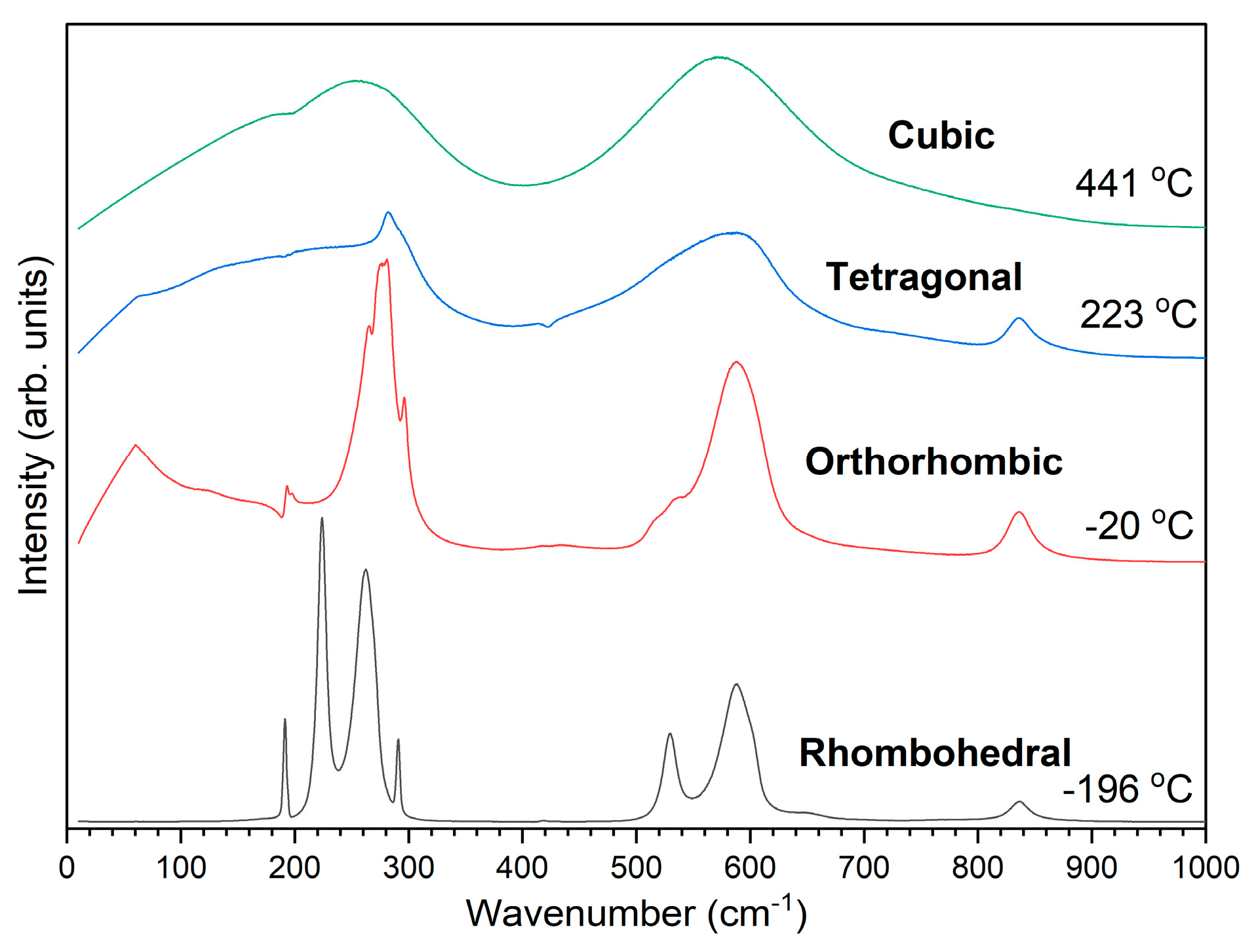
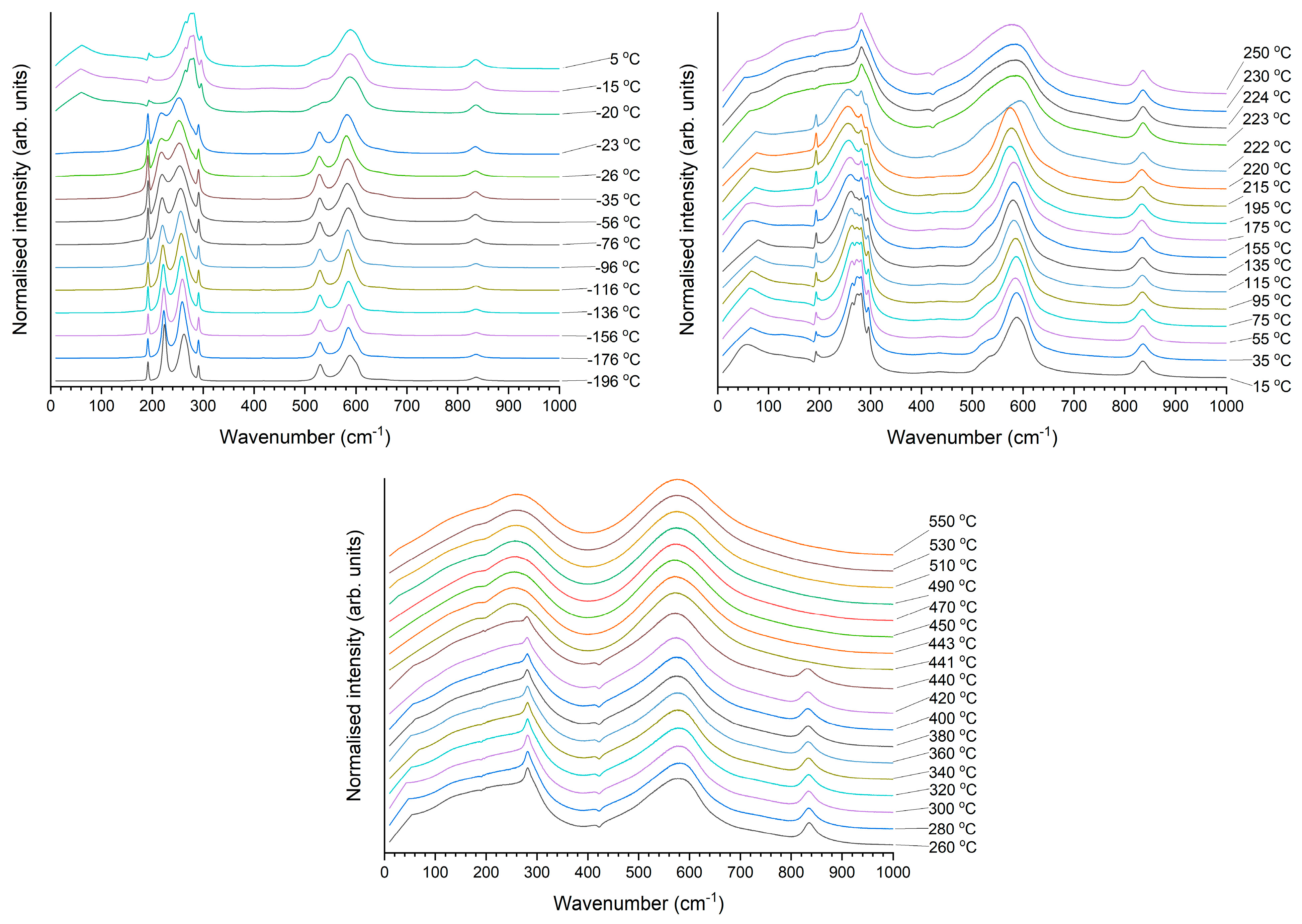
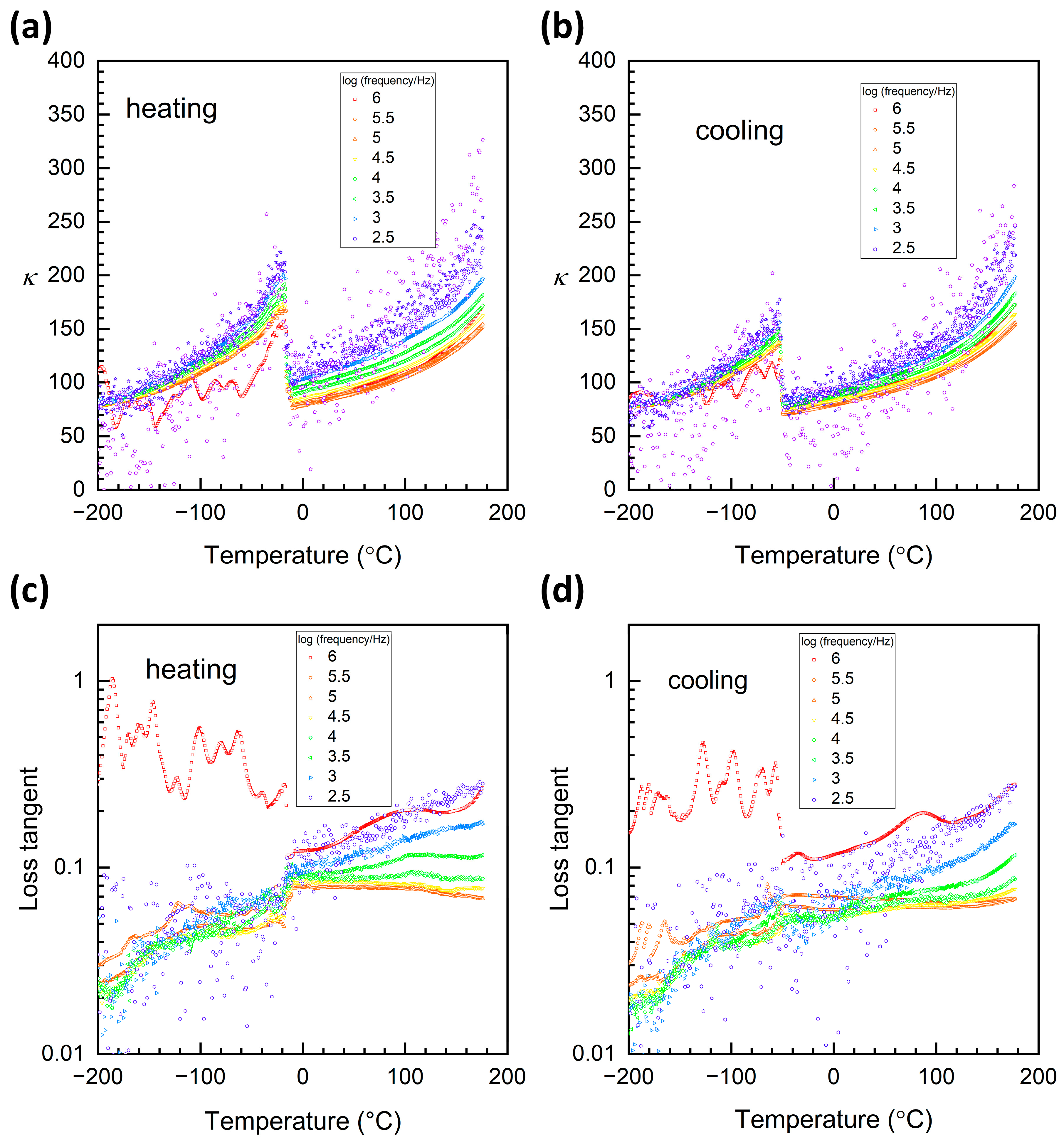
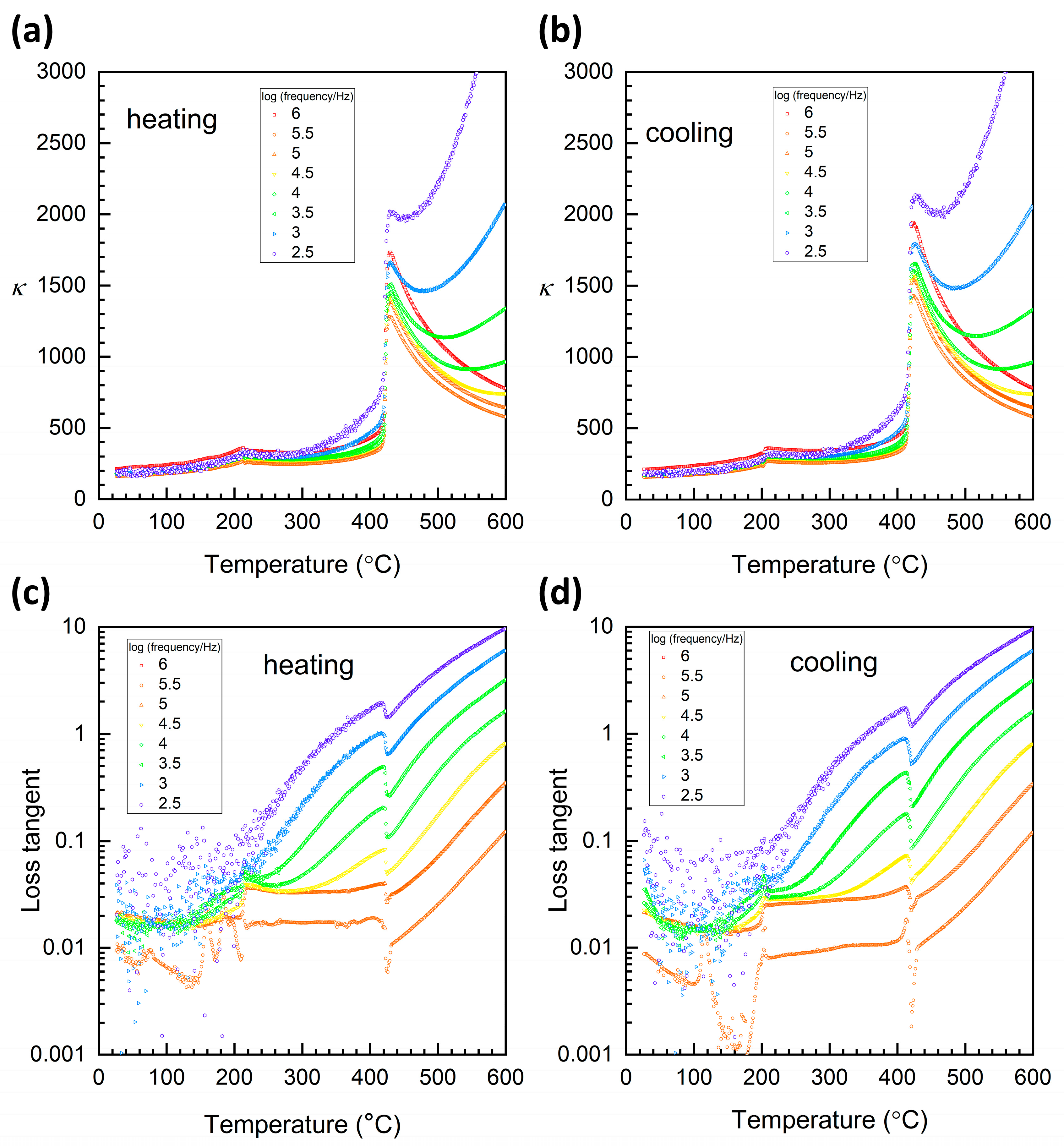
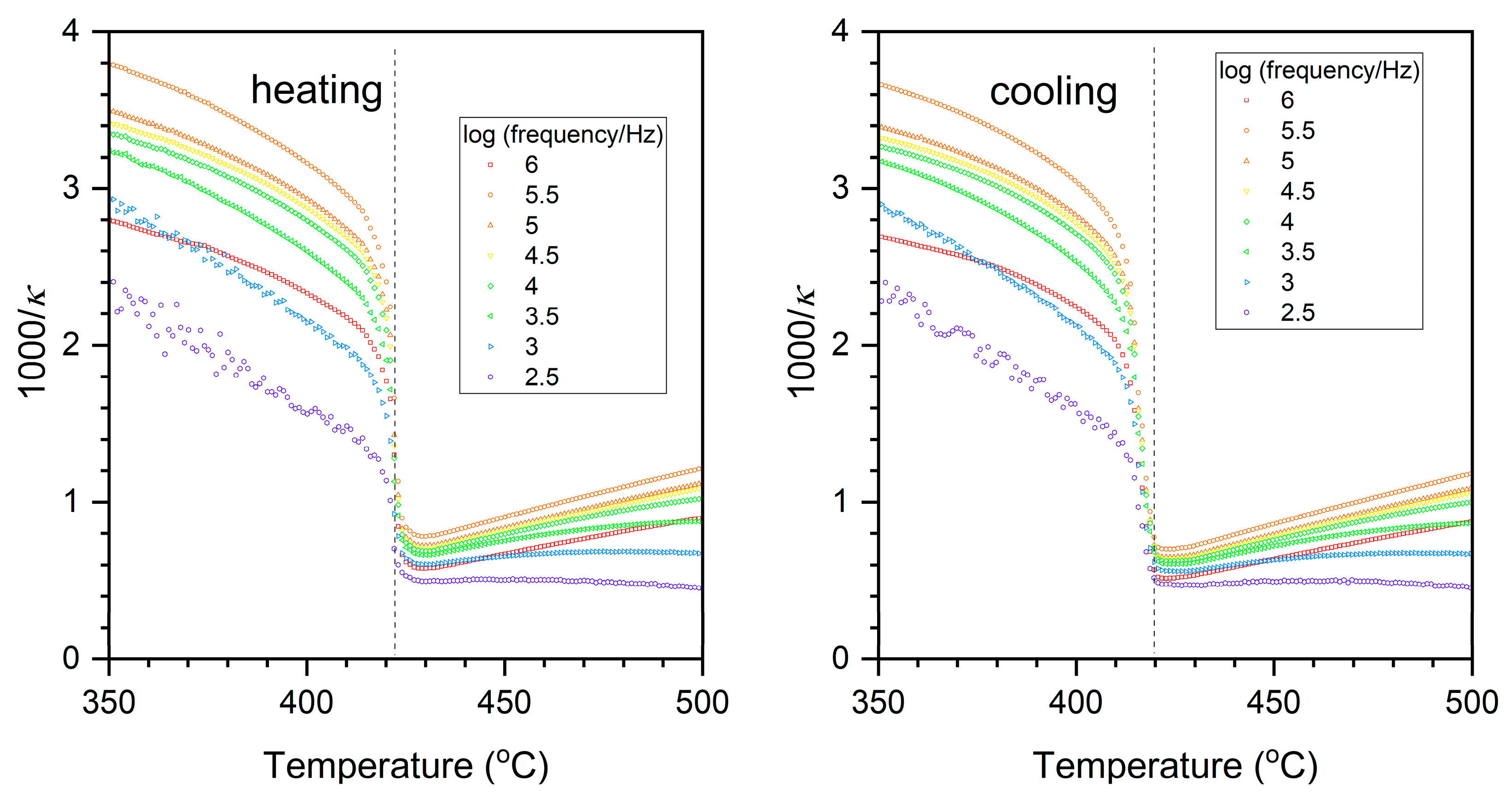
2. Results
3. Discussion
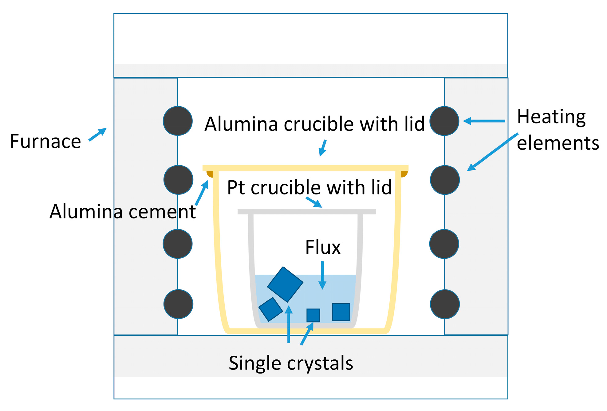
4. Materials and Methods
5. Conclusions
Author Contributions
Funding
Data Availability Statement
Acknowledgments
Conflicts of Interest
References
- Baier-Saip, J.A.; Ramos-Moor, E.; Cabrera, A.L. Raman study of phase transitions in KNbO3. Solid State Commun. 2005, 135, 367–372. [Google Scholar] [CrossRef]
- Wood, E.A. Polymorphism in Potassium Niobate, Sodium Niobate, and other ABO3 Compounds. Acta Crystallogr. 1951, 4, 353–362. [Google Scholar] [CrossRef]
- Shirane, G.; Danner, H.; Pavlovic, A.; Pepinsky, R. Phase Transitions in Ferroelectric KNbO3. Phys. Rev. 1954, 93, 672–673. [Google Scholar] [CrossRef]
- Yoneda, Y.; Ohara, K.; Nagata, H. Local structure and phase transitions of KNbO3. Jpn. J. Appl. Phy. 2018, 57, 11UB07. [Google Scholar] [CrossRef]
- Tennery, V.J.; Hang, K.W. Thermal and X-Ray Diffraction Studies of the NaNbO3–KNbO3 System. J. Appl. Phys. 1968, 39, 4749–4753. [Google Scholar] [CrossRef]
- Jaffe, B.; Cook, W.R.; Jaffe, H. Perovskite Niobates and Tantalates. In Piezoelectric Ceramics; Academic Press: London, UK, 1971; pp. 185–212. [Google Scholar]
- Rödel, J.; Jo, W.; Seifert, K.T.P.; Anton, E.M.; Granzow, T.; Damjanovic, D. Perspective on the Development of Lead-free Piezoceramics. J. Am. Ceram. Soc. 2009, 92, 1153–1177. [Google Scholar] [CrossRef]
- Wu, J.; Xiao, D.; Zhu, J. Potassium–Sodium Niobate Lead-Free Piezoelectric Materials: Past, Present, and Future of Phase Boundaries. Chem. Rev. 2015, 115, 2559–2595. [Google Scholar] [CrossRef] [PubMed]
- Kakimoto, K.-I.; Masuda, I.; Ohsato, H. Ferroelectric and Piezoelectric Properties of KNbO3 Ceramics Containing Small Amounts of LaFeO3. Jpn. J. Appl. Phy. 2003, 42 Pt 1, 6102–6105. [Google Scholar] [CrossRef]
- Kakimoto, K.-i.; Masuda, I.; Ohsato, H. Solid-Solution Structure and Piezoelectric Property of KNbO3 Ceramics Doped with Small Amounts of Elements. Jpn. J. Appl. Phy. 2004, 43, 6706–6710. [Google Scholar] [CrossRef]
- Masuda, I.; Kakimoto, K.-I.; Ohsato, H. Ferroelectric Property and Crystal Structure of KNbO3 Based Ceramics. J. Electroceram. 2004, 13, 555–559. [Google Scholar] [CrossRef]
- Birol, H.; Damjanovic, D.; Setter, N. Preparation and Characterization of KNbO3 Ceramics. J. Am. Ceram. Soc. 2005, 88, 1754–1759. [Google Scholar] [CrossRef]
- Kim, D.-H.; Joung, M.-R.; Seo, I.-T.; Hur, J.; Kim, J.-H.; Kim, B.-Y.; Lee, H.-J.; Nahm, S. Influence of sintering conditions on piezoelectric properties of KNbO3 ceramics. J. Eur. Ceram. Soc. 2014, 34, 4193–4200. [Google Scholar] [CrossRef]
- Park, J.; Kim, D.H.; Lee, T.G.; Cho, S.H.; Park, S.J.; Ryu, J.; Nahm, S. CuO-added KNbO3-BaZrO3 lead-free piezoelectric ceramics with low loss and large electric field-induced strain. J. Am. Ceram. Soc. 2017, 100, 2948–2957. [Google Scholar] [CrossRef]
- Kim, D.-H.; Joung, M.-R.; Seo, I.-T.; Hur, J.; Kim, J.-H.; Kim, B.-Y.; Lee, H.-J.; Nahm, S. Low-Temperature Sintering and Piezoelectric Properties of CuO-Added KNbO3 Ceramics. J. Am. Ceram. Soc. 2014, 97, 3897–3903. [Google Scholar] [CrossRef]
- Davis, M.; Klein, N.; Damjanovic, D.; Setter, N.; Gross, A.; Wesemann, V.; Vernay, S.; Rytz, D. Large and stable thickness coupling coefficients of [001]C-oriented KNbO3 and Li-modified (K,Na)NbO3 single crystals. Appl. Phys. Lett. 2007, 90, 062904. [Google Scholar] [CrossRef]
- Adachi, H.; Wakabayashi, K.; Nishio, M.; Ogawa, H.; Kamakura, T. Fabrication of Ultrasonic Transducers with KNbO3 Piezoelectric Single Crystal for Detecting Harmonic Signals. Jpn. J. Appl. Phy. 2001, 40, 5698. [Google Scholar] [CrossRef]
- Rouffaud, R.; Marchet, P.; Hladky-Hennion, A.C.; Bantignies, C.; Pham-Thi, M.; Levassort, F. Complete electroelastic set for the (YXt)-45° cut of a KNbO3 single crystal. J. Appl. Phys. 2014, 116, 194106. [Google Scholar] [CrossRef]
- Pollard, T.B.; Kenny, T.D.; Vetelino, J.F.; Da Cunha, M.P. Pure SH-SAW propagation, transduction and measurements on KNbO3. IEEE Trans. Ultrason. Ferroelectr. Freq. Control. 2006, 53, 199–208. [Google Scholar] [CrossRef] [PubMed]
- Nakamura, K.; Oshiki, M.; Kitazume, H. SH-mode SAW and its acousto-optic interaction in KNbO3. In Proceedings of the IEEE Ultrasonics Symposium Proceedings (Cat. No. 98CH36102), Sendai, Japan, 5–8 October 1998; Volume 2, pp. 1305–1308. [Google Scholar]
- Yamanouchi, K.; Wagatsuma, Y.; Odagawa, H.; Cho, Y. Single crystal growth of KNbO3 and application to surface acoustic wave devices. J. Eur. Ceram. Soc. 2001, 21, 2791–2795. [Google Scholar] [CrossRef]
- Uematsu, Y. Nonlinear Optical Properties of KNbO3 Single Crystal in the Orthorhombic Phase. Jpn. J. Appl. Phy. 1974, 13, 1362–1368. [Google Scholar] [CrossRef]
- Fluck, D.; Gunter, P. Second-harmonic generation in potassium niobate waveguides. IEEE J. Sel. Top. Quantum Electron. 2000, 6, 122–131. [Google Scholar] [CrossRef]
- Lee, K.J.; Yoon, C.S.; Rotermund, F. Phase Matching Characteristics of Second-Harmonic Generation in Periodic 90°-Domain Structures of KNbO3. Jpn. J. Appl. Phy. 2007, 46, 7317. [Google Scholar] [CrossRef]
- Beckers, L.; Buchal, C.; Fluck, D.; Pliska, T.; Günter, P. Potassium niobate waveguides: He+ implantation in bulk single crystals and pulsed laser deposition of thin films. Mater. Sci. Eng. A 1998, 253, 292–295. [Google Scholar] [CrossRef]
- Irle, E.; Blachnik, R.; Gather, B. The phase diagrams of Na2O and K2O with Nb2O5 and the ternary system Nb2O5-Na2O-Yb2O3. Thermochim. Acta 1991, 179, 157–169. [Google Scholar] [CrossRef]
- Kudo, K.; Kakiuchi, K.; Mizutani, K.; Hoshikawa, K.; Fukami, T. Growth and Characterization of KNbO3 Single Crystal by Vertical Bridgman Method. Ferroelectrics 2005, 323, 157–164. [Google Scholar] [CrossRef]
- Ilangovan, R.; Balakumar, S.; Subramanian, C. Growth and characterisation of KNbO2 single crystals. Mater. Sci. Technol. 1999, 15, 132–136. [Google Scholar] [CrossRef]
- Xing, W.; Looser, H.; Wüest, H.; Arend, H. Progress in KNbO3 crystal growth. J. Cryst. Growth 1986, 78, 431–437. [Google Scholar] [CrossRef]
- Flückiger, U.; Arend, H. On the preparation of pure, doped and reduced KNbO3 single crystals. J. Cryst. Growth 1978, 43, 406–416. [Google Scholar] [CrossRef]
- Durugkar, P.D.; Katpatal, A.G. Growth and characterization of pure, and doped crystals of potassium niobate. J. Cryst. Growth 1996, 162, 161–166. [Google Scholar] [CrossRef]
- Wenshan, W.; Qun, Z.; Zhaohua, G. Investigation of the colour of KNbO3 single crystals grown by the radio-frequency heating Czochralski technique. J. Cryst. Growth 1987, 83, 62–68. [Google Scholar] [CrossRef]
- Takagi, T.; Fujii, T.; Sakabe, Y. Growth and characterization of KNbO3 by vertical Bridgman method. J. Cryst. Growth 2003, 259, 296–301. [Google Scholar] [CrossRef]
- Jiao, X.; Liu, T.; Lu, Y.; Li, Q.; Guo, R.; Wang, X.; Xu, X. Optical Properties of the Oxygen Vacancy in KNbO3 Crystal. J. Electron. Mater. 2020, 49, 2137–2143. [Google Scholar] [CrossRef]
- Varnhorst, T.; Schirmer, O.F.; Hesse, H. Blue coloration of KNbO3 caused by scattering. J. Cryst. Growth 1991, 108, 429–432. [Google Scholar] [CrossRef]
- Tachibana, M. Beginner’s Guide to Flux Crystal Growth; Springer: Tokyo, Japan, 2017. [Google Scholar]
- Bugaris, D.E.; Zur Loye, H.-C. Materials Discovery by Flux Crystal Growth: Quaternary and Higher Order Oxides. Angew. Chem. Int. Ed. 2012, 51, 3780–3811. [Google Scholar] [CrossRef] [PubMed]
- Watanabe, T.; Yabuta, H.; Ueda, M.; Watanabe, M.; Suzuki, T.; Miura, K.; Ito, N.; Kumada, N. Growth of (1-x)NaNbO3–xBaTiO3 Single Crystals by Slow-Cooling and Flux Methods. Jpn. J. Appl. Phy. 2013, 52, 09KC02. [Google Scholar] [CrossRef]
- Dec, J. Real domain structure in orthorhombic phase of NaNbO3 crystals. Cryst. Res. Technol. 1983, 18, 195–204. [Google Scholar] [CrossRef]
- Rudkovskaya, L.M.; Smotrakov, V.G. Thermogravimetric investigation of the KNbO3-KBO2 system. Inorg. Mater. 1982, 18, 911–912. [Google Scholar]
- Smotrakov, V.G.; Raevskij, I.P.; Rudkovskaya, L.M. Potassium metaniobate preparation in K2CO3–Nb2O5, K2CO3–Nb2O5–B2O3 system. Russ. J. Inorg. Chem. 1982, 27, 1875–1877. [Google Scholar]
- Smotrakov, V.G.; Raevskii, I.P.; Rudkovskaya, L.M. Fig. 09401-System KNbO3-KBO2. In ACerS-NIST Phase Equilibria Diagrams Version 3.3.0; Roth, R.S., Ed.; The American Ceramic Society: Westerville, OH, USA, 2010. [Google Scholar]
- Tian, H.; Hu, C.; Meng, X.; Tan, P.; Zhou, Z.; Li, J.; Yang, B. Top-Seeded Solution Growth and Properties of K1–xNaxNbO3 Crystals. Cryst. Growth Des. 2015, 15, 1180–1185. [Google Scholar] [CrossRef]
- Koruza, J.; Liu, H.; Höfling, M.; Zhang, M.-H.; Veber, P. (K,Na)NbO3-based piezoelectric single crystals: Growth methods, properties, and applications. J. Mater. Res. 2020, 35, 990–1016. [Google Scholar] [CrossRef]
- Lee, M. X-ray Diffraction for Materials Research: From Fundamentals to Applications; Apple Academic Press Inc.: Oakville, ON, Canada, 2016; pp. 182–223. [Google Scholar]
- Iamsasri, T.; Tutuncu, G.; Uthaisar, C.; Pojprapai, S.; Jones, J.L. Analysis methods for characterizing ferroelectric/ferroelastic domain reorientation in orthorhombic perovskite materials and application to Li-doped Na0.5K0.5NbO3. J. Mater. Sci. 2013, 48, 6905–6910. [Google Scholar] [CrossRef]
- Ochoa, D.A.; Esteves, G.; Iamsasri, T.; Rubio-Marcos, F.; Fernández, J.F.; García, J.E.; Jones, J.L. Extensive domain wall contribution to strain in a (K,Na)NbO3-based lead-free piezoceramics quantified from high energy X-ray diffraction. J. Eur. Ceram. Soc. 2016, 36, 2489–2494. [Google Scholar] [CrossRef]
- Deng, H.; Zhang, H.; Zhao, X.; Chen, C.; Wang, X.A.; Li, X.; Lin, D.; Ren, B.; Jiao, J.; Luo, H. Direct observation of monoclinic ferroelectric phase and domain switching process in (K0.25Na0.75)NbO3 single crystals. CrystEngComm 2015, 17, 2872–2877. [Google Scholar] [CrossRef]
- Hirohashi, J.; Yamada, K.; Kamio, H.; Uchida, M.; Shichijyo, S. Control of specific domain structure in KNbO3 single crystals by differential vector poling method. J. Appl. Phys. 2005, 98, 034107. [Google Scholar] [CrossRef]
- Skjærvø, S.L.; Høydalsvik, K.; Blichfeld, A.B.; Einarsrud, M.-A.; Grande, T. Thermal evolution of the crystal structure and phase transitions of KNbO3. R. Soc. Open Sci. 2018, 5, 180368. [Google Scholar] [CrossRef] [PubMed]
- Bhattacharjee, S.; Chattopadhyay, K.K. Laser-induced Fano interference subsumed by electron–phonon coupling in orthorhombic KNbO3 nano-bricks: An ab initio vibrational and Raman spectroscopic investigation. J. Raman Spectrosc. 2023, 54, 871–886. [Google Scholar] [CrossRef]
- Qi, W.; Xie, C.; Hushur, A.; Kojima, S. Pressure-induced successive phase transitions and Fano resonance engineering in lead-free piezoceramics KNbO3. Appl. Phys. Lett. 2023, 122, 232901. [Google Scholar] [CrossRef]
- Buixaderas, E.; Nuzhnyy, D.; Gregora, I.; Kamba, S.; Berta, M.; Malic, B.; Kosec, M. Lattice Dynamics and Phase Transitions in KNbO3 and K0.5Na0.5NbO3 Ceramics. IEEE Trans. Ultrason. Ferroelectr. Freq. Control. 2009, 56, 1843–1849. [Google Scholar] [CrossRef] [PubMed]
- Kuzmany, H. Solid-State Spectroscopy; Springer: Berlin/Heidelberg, Germany, 2009. [Google Scholar]
- Połomska, M.; Hilczer, B.; Kosec, M.; Malič, B. Raman Scattering Studies of Lead Free (1-x)K0.5Na0.5NbO3-xSrTiO3 Relaxors. Ferroelectrics 2008, 369, 149–156. [Google Scholar] [CrossRef]
- Trodahl, H.J.; Klein, N.; Damjanovic, D.; Setter, N.; Ludbrook, B.; Rytz, D.; Kuball, M. Raman spectroscopy of (K,Na)NbO3 and (K,Na)1−xLixNbO3. Appl. Phys. Lett. 2008, 93, 262901. [Google Scholar] [CrossRef]
- Klein, N.; Hollenstein, E.; Damjanovic, D.; Trodahl, H.J.; Setter, N.; Kuball, M. A study of the phase diagram of (K,Na,Li)NbO3 determined by dielectric and piezoelectric measurements, and Raman spectroscopy. J. Appl. Phys. 2007, 102, 014112. [Google Scholar] [CrossRef]
- Kodre, A.; Tellier, J.; Arčon, I.; Malič, B.; Kosec, M. Extended x-ray absorption fine structure study of phase transitions in the piezoelectric perovskite K0.5Na0.5NbO3. J. Appl. Phys. 2009, 105, 113528. [Google Scholar] [CrossRef]
- Tsuda, K.; Tanaka, M. Nanometer-scale local structural study of the paraelectric cubic phase of KNbO3 by convergent-beam electron diffraction. Jpn. J. Appl. Phy. 2017, 56, 10PB09. [Google Scholar] [CrossRef]
- Fridkin, V.M. Ferroelectric Semiconductors; Consultants Bureau: New York, NY, USA, 1980. [Google Scholar]
- Lines, M.E.; Glass, A.M. Principles and Applications of Ferroelectrics and Related Materials; Oxford University Press: Oxford, UK, 2001. [Google Scholar]
- Shannon, R.D. Revised effective ionic radii and systematic studies of interatomic distances in halides and chalcogenides. Acta Crystallogr. A 1976, 32, 751–767. [Google Scholar] [CrossRef]
- Bruker-AXS. APEX2; Version 2014.11-0; Bruker-AXS: Madison, WI, USA, 2014. [Google Scholar]
- Krause, L.; Herbst-Irmer, R.; Sheldrick, G.M.; Stalke, D. Comparison of silver and molybdenum microfocus X-ray sources for single-crystal structure determination. J. Appl. Crystallogr. 2015, 48, 3–10. [Google Scholar] [CrossRef] [PubMed]
- Sheldrick, G. Crystal structure refinement with SHELXL. Acta Cryst. C 2015, 71, 3–8. [Google Scholar] [CrossRef]
- Dolomanov, O.V.; Bourhis, L.J.; Gildea, R.J.; Howard, J.A.K.; Puschmann, H. OLEX2: A complete structure solution, refinement and analysis program. J. Appl. Crystallogr. 2009, 42, 339–341. [Google Scholar] [CrossRef]
- Svitelskiy, O.; Toulouse, J.; Yong, G.; Ye, Z.G. Polarized Raman study of the phonon dynamics in Pb(Mg1/3Nb2/3)O3 crystal. Phys. Rev. B 2003, 68, 104107. [Google Scholar] [CrossRef]


| Crystal 2a | Crystal 2b | |||||||
|---|---|---|---|---|---|---|---|---|
| Miller indices | 101 | 010 | 202 | 020 | 101 | 010 | 202 | 020 |
| Peak position (2θ) | 21.98 | 22.35 | 44.83 | 45.60 | 22.03 | 22.37 | 44.93 | 45.66 |
| d-spacing (Å) | 4.0434 | 3.9777 | 2.0218 | 1.9893 | 4.0348 | 3.9740 | 2.0176 | 1.9868 |
| Space Group Crystal System | Orthorhombic |
|---|---|
| Space group name | Cmm2 (no. 35) |
| Unit cell length a | 5.660(1) Å |
| Unit cell length b | 5.664(1) Å |
| Unit cell length c | 4.027(1) Å |
| Unit cell angle α | 90° |
| Unit cell angle β | 90° |
| Unit cell angle γ | 90° |
| Unit cell volume | 129.09(5) Å3 |
| Formula units (Z) | 2 |
| Calculated density | 4.631 g/cm3 |
| Oxide | Sample 1 (mol %) | Sample 2 (mol %) | Nominal Composition (mol %) |
|---|---|---|---|
| K2O | 50.00 ± 0.19 | 48.53 ± 0.28 | 50 |
| Nb2O5 | 49.75 ± 0.19 | 49.83 ± 0.48 | 50 |
| B2O3 | 0.25 ± 0.32 | 1.63 ± 0.61 | - |
| Al2O3 | Not measured | 0.01 ± 0.01 | - |
Disclaimer/Publisher’s Note: The statements, opinions and data contained in all publications are solely those of the individual author(s) and contributor(s) and not of MDPI and/or the editor(s). MDPI and/or the editor(s) disclaim responsibility for any injury to people or property resulting from any ideas, methods, instructions or products referred to in the content. |
© 2024 by the authors. Licensee MDPI, Basel, Switzerland. This article is an open access article distributed under the terms and conditions of the Creative Commons Attribution (CC BY) license (https://creativecommons.org/licenses/by/4.0/).
Share and Cite
Doan, T.T.; Fisher, J.G.; Lee, J.-S.; Tran, H.T.; Gao, J.; Mok, J.; Lee, J.; Benčan, A.; Dražić, G.; Junaid, S.B.; et al. Growth of KNbO3 Single Crystals by the Flux Method Using KBO2 as a Flux. Inorganics 2024, 12, 151. https://doi.org/10.3390/inorganics12060151
Doan TT, Fisher JG, Lee J-S, Tran HT, Gao J, Mok J, Lee J, Benčan A, Dražić G, Junaid SB, et al. Growth of KNbO3 Single Crystals by the Flux Method Using KBO2 as a Flux. Inorganics. 2024; 12(6):151. https://doi.org/10.3390/inorganics12060151
Chicago/Turabian StyleDoan, Thanh Trung, John G. Fisher, Jong-Sook Lee, Huyen Tran Tran, Jie Gao, Jungwi Mok, Junseong Lee, Andreja Benčan, Goran Dražić, Syed Bilal Junaid, and et al. 2024. "Growth of KNbO3 Single Crystals by the Flux Method Using KBO2 as a Flux" Inorganics 12, no. 6: 151. https://doi.org/10.3390/inorganics12060151