Article

Some Aspects of Hot Carrier Photocurrent across GaAs p-n Junction

by
Steponas Ašmontas
1,*,
Oleksandr Masalskyi
2,*,
Ihor Zharchenko
1,2,
Algirdas Sužiedėlis
1 and
Jonas Gradauskas
1,2
1
Laboratory of Electronic Processes, Center for Physical Sciences and Technology, LT-10257 Vilnius, Lithuania
2
Department of Physics, Vilnius Gediminas Technical University, LT-10223 Vilnius, Lithuania
*
Authors to whom correspondence should be addressed.
Inorganics 2024, 12(6), 174; https://doi.org/10.3390/inorganics12060174
Submission received: 7 May 2024 / Revised: 4 June 2024 / Accepted: 14 June 2024 / Published: 20 June 2024
(This article belongs to the Special Issue Optical and Quantum Electronics: Physics and Materials)

Abstract

:
The photocurrent across crystalline GaAs p-n junction induced by Nd:YAG laser radiation was investigated experimentally. It is established that the displacement current is dominant at reverse and low forward bias voltages in the case of pulsed excitation. This indicates that hot carriers do not have enough energy to overcome the p-n junction until the forward bias significantly reduces the potential barrier. At a sufficiently high forward bias, the photocurrent is determined by the diffusion of hot carriers across the p-n junction. The current–voltage (I-V) characteristics measured at different crystal lattice temperatures show that the heating of carriers by laser radiation increases with a drop in crystal lattice temperature. This study proposes a novel model for evaluating carrier temperature based on the temperature coefficient of the I-V characteristic. It is demonstrated that the heating of carriers by light diminishes the conversion efficiency of a solar cell, not only through thermalisation but also because of the conflicting interactions between the hot carrier and conventional photocurrents, which exhibit opposite polarities. These findings contribute to an understanding of hot carrier phenomena in photovoltaic devices and may prompt a revision of the intrinsic losses in solar cells.

1. Introduction

The ambition to reduce the difference between the theoretically predicted and practically achieved efficiencies of a solar cell requires the introduction of new physical concepts. Hot carriers (HCs) are one of the modern candidates for solving this problem. Hot carriers are free carriers with excess energy higher than the crystal lattice temperature. In a semiconductor, light can heat the carriers in two cases. First, if the light photon energy h v is lower than the bandgap E g , heating results from intraband absorption. Such free carrier absorption is not spectrally selective and follows the classical Drude–Zener ∝ λ 2 law ( λ is the light wavelength) [1]. The HC photocurrent induced by below-bandgap photons was studied in Si, Ge, and GaAs p-n [2,3,4], and n-n+ and p-p+ [5] diodes exposed to CO2 laser radiation ( h v = 0.12 eV). The polarity of the HC photocurrent indicates carrier flow up the potential barrier. Another possibility for creating hot carriers is the interband absorption of photons with energy h v > E g . The excess energy, h v E g , is given to the generated electron or hole. Independent of excitation, HCs dissipate their energy through carrier–phonon and carrier–carrier scattering events. This process is defined by the energy relaxation time, which is typically on a picosecond scale [6].
The role of hot carriers in photovoltaics remains unclear. On the one hand, classical calculations of the possible efficiency of a solar cell ignore intraband absorption, which is treated as an intrinsic “below  E g  loss” [7,8]. The indirect harmful impact of HCs on the operation of a cell is considered only as a “thermalisation loss”; that is, their excess energy heats the crystal lattice and hence leads to efficiency loss.
On the other hand, HCs are evidenced in solar cells, and despite their extremely short lifetime, they provide benefits. For example, excess energy in hot carriers can be optically eliminated by the emission of infrared photons [9], or used for photon upconversion [10]. Direct energy harvesting before thermalisation can be realised by impact ionisation [11,12], nanowire-modified phononic properties leading to increased relaxation times [13], or extraction of excess energy through contacts [14,15,16]. Extraction of hot electrons near the collector results in an increased open-circuit voltage of an ultrathin p-i-n cell [14]. If an energy-selective contact is made up of many contacts with particular energy differences, collecting HCs through it enhances the efficiency of a single-bandgap p-i-n solar cell both by using the extra energy of HCs and by avoiding lattice heating [15]. An efficient hot carrier solar cell, a cell based entirely on the HC phenomenon, was proposed [17]. According to theoretical calculations by Ross and Nozik, the conversion efficiency of HC solar cells can reach 60%. More recently, a large number of theoretical and experimental studies devoted to the development of HC solar cells were carried out [18,19,20,21,22,23,24,25,26,27,28,29]. But until now, no HC solar cell valuable for practical application has been created.
To understand and rule HC processes in semiconductors, knowledge of carrier temperature becomes a key parameter. Various techniques were developed to determine the temperature of the hot carriers. Ultrafast pump–probe spectroscopy [27,28], spontaneous photoemission spectroscopy [29], electrical measurements [30], steady-state photoluminescence spectroscopy [31], theoretical considerations [32] and other studies provide insights into the thermodynamic characteristics of the carriers.
This study presents the hot carrier photocurrent induced by close-to-bandgap laser light across a GaAs p-n diode. A model of the temperature coefficient of the voltage changes of the current–voltage characteristic is used to obtain the HC temperature. The distribution of ‘cold’ and hot carriers is analysed with regard to the potential barrier height of the p-n junction. The impact of HC on photovoltage formation in solar cells is discussed

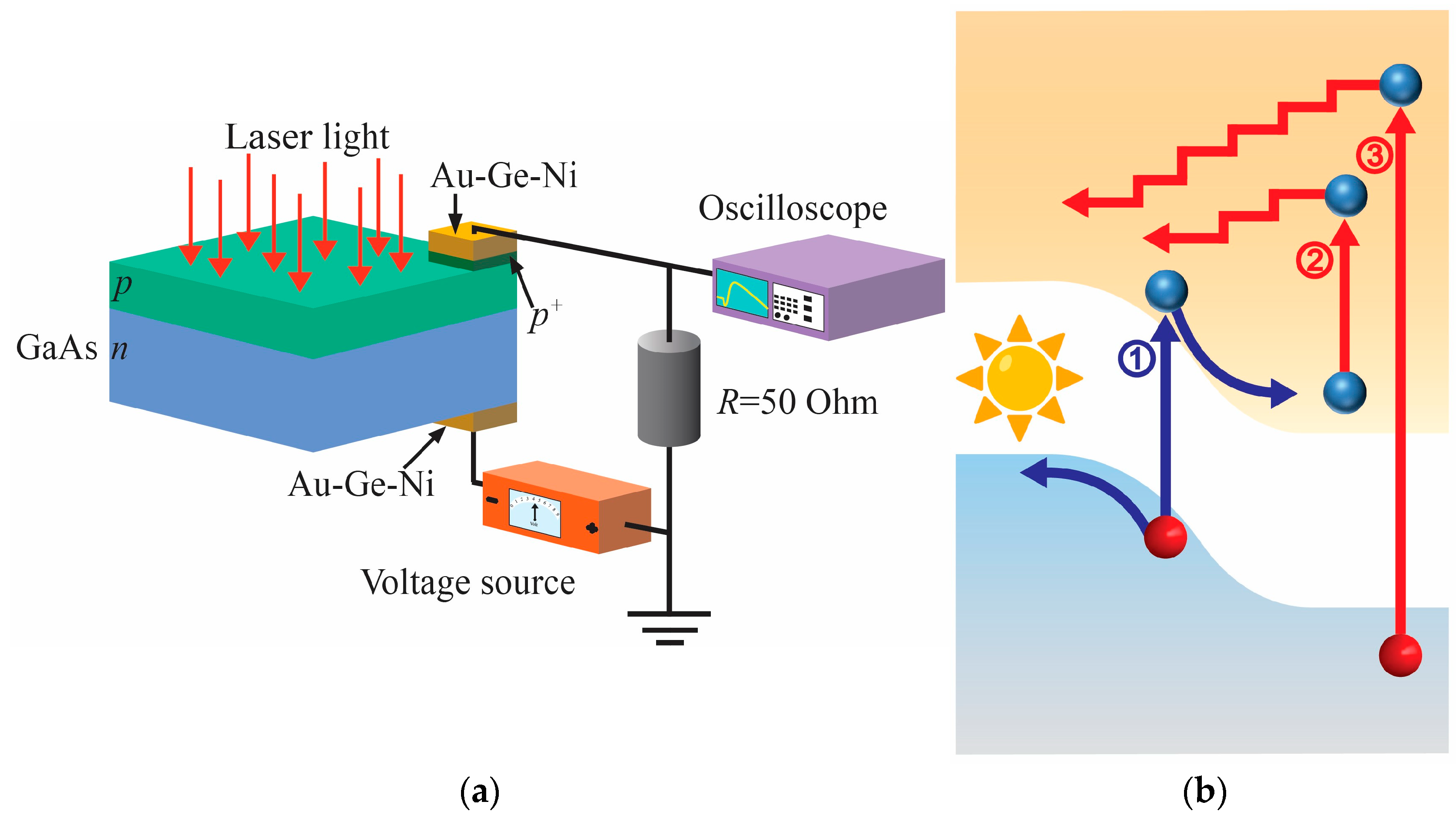
2. Materials and Methods
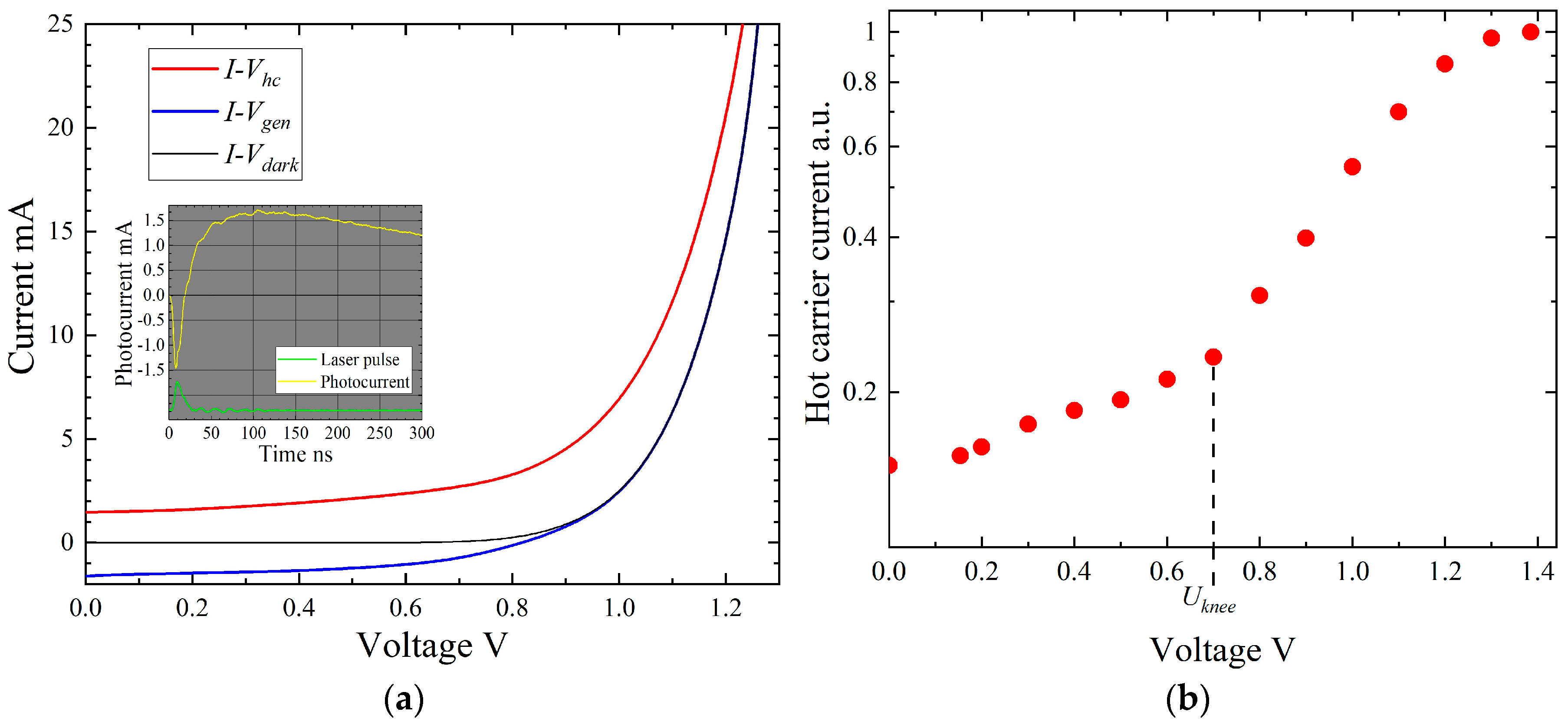
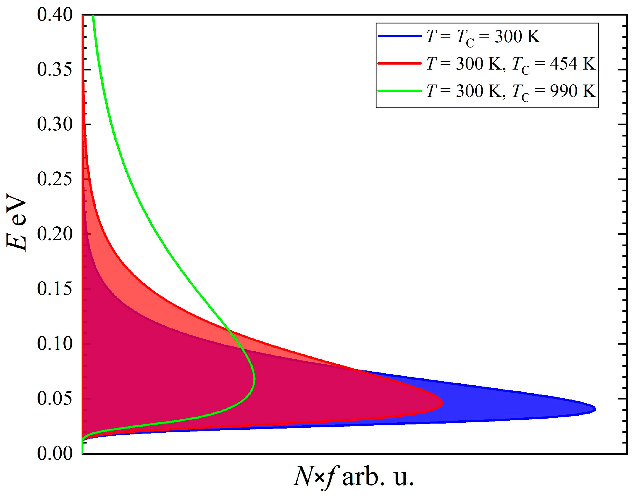
The GaAs p-n junction was a 5 µm thick liquid-phase epitaxy-grown p-type layer on an n-type substrate with respective 5 × 1017 cm−3 and 3 × 1017 cm−3 hole and electron densities. For better ohmic contact, a thin heavily doped p+-layer with a 2 × 1018 cm−3 hole density was additionally grown (see Figure 1a). The fabrication process involved traditional photolithography techniques finalised by thermal evaporation and standard annealing of the Au–Ge–Ni ohmic contacts. To avoid direct illumination and the rise of unwanted photosignals across the top p-p+ and semiconductor–metal contacts, the p+-layer was etched off, leaving it only below the metal contacts, and the contacts were positioned at the periphery of the 2.5 × 2.5 mm2 cut sample (Figure 1a). Laser light of 1.064 μm wavelength, 17 ns long pulses, 50 Hz repetition rate, and 0.7 MW/cm2 intensity was used for excitation (Nd:YAG laser fabricated by Ekspla Ltd., Vilnius, Lithuania). The material was chosen because of its bandgap E g = 1.42 eV, which is close to the bandgap of a solar cell with maximum possible efficiency [8], and because single-crystal single-junction solar cells demonstrate higher efficiency as compared to multicrystalline or thin-film solar cells [33]. In addition, to evidence the hot carrier effect, the GaAs bandgap was wider than the laser light photon energy h v = 1.17 eV.
The experiment was conducted under the photocurrent regime, where the photovoltage across the 50-Ohm load resistor was measured using a digital oscilloscope from Agilent Technologies DSO6102A (Santa Rosa, CA, USA) as shown in Figure 1a. The photoresponse consisted of two components of opposite polarity (see the inset in Figure 2a). The peak value of each photocurrent subpulse induced by pulsed laser light was measured and used for analysis. The research was carried out at 300 K and 80 K temperatures.

3. Results

When the GaAs p-n junction is exposed to pulsed 1.064 μm laser light, the induced photocurrent, on the whole, consists of three components defined by carrier generation, hot carriers, and lattice heating [34]. Since the photon energy is lower than the semiconductor bandgap, the generated current results from interband two-photon absorption [35]. The polarity of the two heating-associated photocurrent components is opposite to that of the generation. Specifically, the diffusion of high-energy carriers across the junction against the built-in electric field is caused by the carrier density gradient, and it initiates the hot carrier photocurrent, as shown by the red stepped arrows in Figure 1b. At the same time, the heated lattice-induced change in the potential barrier results in the redistribution of charges and, thus, carrier transport in the same direction. The source of carrier heating is dual. First, it is determined by the free carrier absorption of the below-bandgap photons (Figure 1b, process 2). Second, they are heated by the energy 2 h v E g = 0.91 eV left over from electron–hole generation (process 3). Until they dissipate their excess energy, the HCs can diffuse toward the junction barrier, thus forming the HC photocurrent. Calculation of the hot carrier diffusion length,
L D = D τ ε ,
reveals that it is of the order of 100–150 nm; using approximate values of the diffusion coefficient D ≤ 200 cm2/s, and the carrier energy relaxation time τ ε = 1 ps [6], we obtain L D = 141 nm. This is comparable to the width of the depleted region of the junction W  = 100 nm [36]. Thus, this version of hot carrier transport over the p-n junction, as previously believed [2], seems reasonable.
In this work, the negative (see inset in Figure 2a) photocurrent component is attributed to the hot carrier effect because of (a) its fast run determined by the carrier energy relaxation time, and (b) polarity corresponding to the carrier flow up the barrier of the p-n junction, as indicated by red stepped arrows in Figure 1b, and its rise with increasing forward bias. The role of the lattice heating-caused component was ignored because of its relatively small input into the net photocurrent, as shown earlier [34]. Due to their opposite polarities, competition between the generation (blue) and hot carrier (red) photocurrents is seen in the I-V characteristics, and both of them are influenced by the bias voltage (Figure 2a).
The HC photocurrent increases with the forward voltage (Figure 2b). At a particular voltage of 0.7 V (the ‘knee’ voltage), the dependence shows a typical turning point when the hot carrier photocurrent starts to grow sharply. This sudden exponential rise of the HC photocurrent was explained by the change in the photocapacitive nature of the pulsed displacement current at reverse and low-forward-bias voltage to the flow of hot carriers across the bias-lowered p-n junction barrier [37,38]. The displacement HC photocurrent is analogous to the AC current across a capacitor; it is present only in the case of pulsed carrier heating and resulting recharging of the junction. A similar HC-caused displacement current was also observed across an MOS structure [39]. A further increase in the forward bias leads to saturation of the HC photocurrent because of the reduced potential barrier and Joule’s heating effect [2].
The potential barrier height is also influenced by the temperature of the diode. Figure 3 shows the I-V curves at room and liquid nitrogen temperatures. The shift of the I-Vs with temperature change can be described by the temperature coefficient, which is a material-specific parameter and is associated with electronic components whose characteristics are temperature-dependent [15,28,40].
The temperature coefficient indicates the voltage change per temperature degree at a fixed current value [41]:
α T = Δ U Δ T i = c o n s t . ,
where Δ U is the voltage change, and Δ T is the corresponding change in temperature. Using the data in Figure 3, we obtain
α T = U N 2 d a r k U R d a r k 80 K 300 K = 2 . 14   mV K i = 42 . 7   mA cm 2 .
The reason for choosing the 42.7 mA·cm–2 current density as a fixed one is described in the next paragraph. The obtained value of the temperature coefficient falls within the −(1.88–2.30) mV/K range announced for GaAs solar cells [42], and is close to −2.37 mV/K of GaAs diodes, as calculated using data from ref. [43]. In Equation (3) and elsewhere, the index “dark” indicates the voltage of the unilluminated diode, and the indices “N2” and “R” represent liquid nitrogen and room temperature, respectively.
As Figure 3 shows, the dark current can be assumed to still be equal to zero at the mentioned ‘knee’ voltage of 0.7 V, and the corresponding 42.7 mA·cm–2 current density in the I-Vhc is determined entirely by the hot carriers (Figure 3). This point of the I-Vhc contains information about the carrier temperature. As the forward bias voltage increases further, the total current starts to consist of both the dark current and the HC photocurrent. Fixing this 42.7 mA·cm–2 value as a constant both for the illuminated and dark cases, and assuming that both these currents, the dark and HC, are of the same (recombination) nature, as explained below, we calculate the difference between the carrier and lattice temperatures, Δ T C , under room temperature conditions using the obtained temperature coefficient α T = −2.14 mV·K–1:
Δ T C = U R d a r k U R h c α T = 154   K   i = 42 . 7   mA cm 2 ,
where U R h c = 0.70 V, U R d a r k = 1.03 V, and the index “hc” refers to the I-Vhc of the hot carriers. The same approach was used to calculate the HC temperature under the liquid nitrogen conditions assuming the same constant current density value of 42.7 mA·cm−2 at respective voltage values of U N 2 h c = 1.10 V (illuminated case, pure hot carrier current) and U N 2 d a r k = 1.50 V (dark current). As a result, Δ T C  = 187 K at T = 80 K. These findings indicate that the carrier heating process is more pronounced at lower temperatures, which is probably related to the increase in the carrier energy relaxation time constant at lower temperatures [6]. The proposed model for evaluating carrier temperature is supported by the following sequential reasoning: the stronger the heating, the stronger the hot carrier current, and the higher the upward shift of the current–voltage characteristic (see red lines in Figure 2a and Figure 3). Higher shift is followed by a bigger difference in voltage values and, according to Equation (4), leads to a higher value of Δ T C . The results obtained using the temperature coefficient method agree with the findings reported in other studies, as summarised in Table 1.
The estimated hot carrier temperature provides an additional tool to investigate the dynamics of hot carriers in a p-n junction. In general, the density of states occupied by free electrons in the conduction band is expressed as [36]
n ( E ) = N ( E ) × f ( E ) ,
where f ( E ) is the Fermi–Dirac probability function, and N ( E ) is the density of states in the conduction band. After making all the necessary substitutions [36], Equation (5) becomes
n ( E ) = N C E E C 4 π 3.5 k 3.5 T 1.5 × 1 1 + exp E E F k T C ,
where E C = 0 eV is the energy of the conduction band bottom, N C is the effective density of states in the conduction band, T is the lattice temperature, T C is the carrier temperature, E is the energy (in eV), E F is the Fermi level, and k is the Boltzmann constant.
The blue area in Figure 4 shows the electron distribution in the conduction band calculated in the case of no excitation, i.e., at T = T C = 300 K. The data needed for the calculation were taken from ref. [6]. When the carriers are heated, in our case, we obtain a hot electron distribution using T C = 454 K in the Fermi–Dirac probability function of Equation (6) at a T = 300 K lattice temperature (red area). Naturally, the ‘tail’ of the HC distribution is now extended to higher energies. However, its value is fading away at a level that is much lower than the unbiased potential barrier of the junction, 1.31 eV, and is still lower than the 0.7 V forwardly biased barrier of 1.31 eV − 0.7 eV = 0.61 eV. Statistically, only 10–4% of the hot electrons, or of the total red area in Figure 4, are above the 0.61 eV energy level. Thus, the probability that a hot electron will form a current by overcoming the barrier is negligibly small. Similar results are obtained for the hot hole distribution in the valence band, and similar barrier-related considerations can be applied to the hot holes. This means that the hot carrier photocurrent across the p-n junction at reverse and low-forward-bias voltages cannot be a diffusion of the HCs over the barrier, as was supposed earlier [2] and is schematised in Figure 1b. Therefore, the hot carrier photocurrent changes its nature from a displacement character to a recombination character when the ‘knee’ voltage is exceeded. Still being well below the top of the barrier, the hot carriers do not manage to overcome it, as the calculated carrier distribution shows, but now, the heated electrons and holes can meet each other in the depleted region and recombine, thus forming the recombination current. However, at higher voltages, the HC photocurrent most probably turns into diffusion of the hot carriers over the substantially reduced potential barrier. To reach the same 42.7 mA·cm–2 recombinative photocurrent across the unbiased potential barrier, or, in other words, to obtain 10–4% of hot electrons above the energy level of 1.31 eV, the electron temperature should be approximately 990 K.
In the case of sunlight-illuminated solar cells, the potential barrier of the p-n junction decreases due to generated electron–hole pairs, thereby creating favourable conditions for the HC current flow through the junction. Since the generation-related photocurrent and HC photocurrent flow in opposing directions, it is evident that carrier heating diminishes the overall current passing through the p-n junction, thereby decreasing the conversion efficiency of a solar cell.

4. Conclusions

In conclusion, we analysed the hot carrier photocurrent induced across the GaAs p-n junction by the 1.064 μm laser radiation. Based on earlier studies and this study, the hot carrier photocurrent, in contrast to traditional assumptions, has three stages: (1) displacement current at low bias voltage in the case of pulsed excitation, (2) recombination current at higher forward bias exceeding the ‘knee’ voltage, and (3) diffusion current, which is possible only in the case of a strong excitation level resulting in high carrier temperature and at a high enough forward bias allowing the hot carriers to overcome the potential barrier. On the basis of the temperature coefficient of the current–voltage characteristics, we propose a novel technique to estimate the hot carrier temperature. The result of the calculation falls within the reasonable range of carrier temperatures obtained by other methods. A more substantial change in the absolute hot carrier temperature at liquid nitrogen temperature compared with room temperature implies that carrier heating is stronger at lower lattice temperatures because of the longer energy relaxation time of the hot carriers.
Concerning solar photovoltaics, several points based on the results are worth noting. The hot carrier photocurrent flows in a direction opposite to the functional generation current, and this way, it can have a detrimental impact on the operation of a solar cell; it should be considered an additional intrinsic “pre-thermalisational loss”. Absorption of the below-bandgap radiation also causes carrier heating and cannot be neglected. Although this study focuses on the hot carrier effect caused by single-wavelength radiation at intensities much higher than sunlight, hot carriers will still have a certain impact when considering the entire solar spectrum. These findings contribute to a deeper understanding of the hot carrier phenomena in single-junction solar cells and will probably facilitate a quicker alignment between theoretically predicted and practically achieved solar cell efficiencies.

Author Contributions

Conceptualisation, O.M., J.G. and S.A.; methodology, O.M., J.G., A.S. and S.A.; software, O.M. and I.Z.; validation, O.M., J.G. and S.A.; formal analysis, A.S., J.G. and S.A.; investigation, O.M. and I.Z.; resources, A.S.; data curation, O.M., J.G. and I.Z.; writing—original draft preparation, O.M.; writing—review and editing, J.G. and S.A.; visualisation, O.M. and J.G.; supervision, J.G. All authors have read and agreed to the published version of the manuscript.

Funding

This research received no external funding.

Data Availability Statement

The original contributions presented in the study are included in the article; further inquiries can be directed to the corresponding author.

Conflicts of Interest

The authors declare no conflicts of interest.

References

  1. Murray, R. Infrared Absorption and Energy Levels Due to Impurities. In Properties of Gallium Arsenide, 3rd ed.; Brozel, M.R., Stillman, G.E., Eds.; The Institution of Electrical Engineers INSPEC: London, UK, 1996; pp. 225–256. [Google Scholar]
  2. Umeno, M.; Sugito, Y.; Jimbo, T.; Hattori, H.; Amenixa, Y. Hot photo-carrier and hot electron effects in p-n junctions. Solid-State Electron. 1978, 21, 191–195. [Google Scholar] [CrossRef]
  3. Encinas-Sanz, F.; Guerra, J.M. Laser-induced hot carrier photovoltaic effects in semiconductor junctions. Prog. Quantum Electron. 2003, 27, 267–294. [Google Scholar] [CrossRef]
  4. Ašmontas, S.; Gradauskas, J.; Seliuta, D.; Širmulis, E. Photoelectrical properties of nonuniform semiconductor under infrared laser radiation. In Proceedings of the International Conference on Nonresonant Laser-Matter Interaction, St. Petersburg, Russia, 21–23 August 2000. [Google Scholar]
  5. Ašmontas, S.; Gradauskas, J.; Seliuta, D.; Šilėnas, A.; Širmulis, E.; Marmur, I.Y. Photoelectrical properties of nonuniform GaAs structures under infrared laser illumination. In Proceedings of the International Conference on SPIE: Nonresonant Laser-Matter Interaction, St. Petersburg, Russia, 1–3 July 1996. [Google Scholar]
  6. Dargys, A.; Kundrotas, J. Physical data for gallium arsenide. 143–188. In Handbook on the Physical Properties of Ge, Si, GaAs and InP, 1st ed.; Science and Encyclopedia: Vilnius, Lithuania, 1994. [Google Scholar]
  7. Shockley, W.; Queisser, H. Detailed Balance Limit of Efficiency of p-n Junction Solar Cells. J. Appl. Phys. 1961, 32, 510–519. [Google Scholar] [CrossRef]
  8. Hirst, L.C.; Ekins-Daukes, N.J. Fundamental losses in solar cells. Prog. Photovolt. Res. Appl. 2011, 19, 286–293. [Google Scholar] [CrossRef]
  9. Saeed, S.; de Jong, E.M.L.D.; Dohnalova, K.; Gregorkiewicz, T. Efficient optical extraction of hot-carrier energy. Nat. Commun. 2014, 5, 4665. [Google Scholar] [CrossRef] [PubMed]
  10. Torchynska, T.V.; Vivas Hernandez, A.; Goldstein, Y.; Jedrzejewskii, J.; Jimenez Sandoval, S. Photoluminescence of Si or Ge nanocrystallites embedded in silicon oxide. J. Non-Cryst. Solids 2006, 352, 1152–1155. [Google Scholar] [CrossRef]
  11. Kolodinski, S.; Werner, J.H.; Wittchen, T.; Queisser, H.J. Quantum efficiencies exceeding unity due to impact ionization in silicon solar cells. Appl. Phys. Lett. 1993, 63, 2405–2407. [Google Scholar] [CrossRef]
  12. Wurfel, P. Solar energy conversion with hot electrons from impact ionisation. Sol. Energy Mater. Sol. Cells 1997, 46, 43–52. [Google Scholar] [CrossRef]
  13. Fast, J.; Aeberhard, U.; Bremner, S.P.; Linke, H. Hot-carrier optoelectronic devices based on semiconductor nanowires. Appl. Phys. Rev. 2021, 8, 021309. [Google Scholar] [CrossRef]
  14. Kempa, K.; Naughton, M.J.; Ren, Z.F.; Herczynski, A.; Kirkpatrick, T.; Rybczynski, J.; Gao, Y. Hot electron effect in nanoscopically thin photovoltaic junctions. Appl. Phys. Lett. 2009, 95, 233121–2331214. [Google Scholar] [CrossRef]
  15. Shayan, S.; Matloub, S.; Rostami, A. Efficiency enhancement in a single bandgap silicon solar cell considering hot-carrier extraction using selective energy contacts. Opt. Express 2021, 29, 5068–5080. [Google Scholar] [CrossRef] [PubMed]
  16. Esgandari, M.; Barzinjy, A.A.; Rostami, A.; Rostami, G.; Dolatyari, M. Solar cells efficiency enhancement using multilevel selective energy contacts (SECs). Opt. Quantum Electron. 2022, 54, 1–9. [Google Scholar] [CrossRef]
  17. Ross, R.T.; Nozik, A.J. Efficiency of hot-carrier solar energy converters. J. Appl. Phys. 1982, 53, 3813–3818. [Google Scholar] [CrossRef]
  18. Neges, M.; Schwarzburg, K.; Willig, F. Monte Carlo simulation of energy loss and collection of hot charge carriers, first step towards a more realistic hot-carrier solar energy converter. Sol. Energy Mater. Sol. Cells 2006, 90, 2107–2128. [Google Scholar] [CrossRef]
  19. Conibeer, G.; Ekins-Daukes, N.; Guillemoles, J.-F.; Konig, D.; Cho, E.-C.; Jiang, C.-W.; Shrestha, S.; Green, M.A. Progress on hot carrier cells. Sol. Energy Mater. Sol. Cells 2009, 93, 713–719. [Google Scholar] [CrossRef]
  20. Le Bris, A.; Guillemoles, J.-F. Hot carrier solar cells: Achievable efficiency accounting for heat losses in the absorber and through contacts. Appl. Phys. Lett. 2010, 97, 113506. [Google Scholar] [CrossRef]
  21. Kirk, A.P.; Fischetti, M.V. Fundamental limitations of hot-carrier solar cells. Phys. Rev. B Condens. Matter. 2012, 86, 165206. [Google Scholar] [CrossRef]
  22. Rodiere, J.; Lombez, L.; Le Corre, A.; Durand, O.; Guillemoles, J.-F. Experimental evidence of hot carrier solar cell operation in multi-quantum wells heterostructures. Appl. Phys. Lett. 2015, 106, 183901. [Google Scholar] [CrossRef]
  23. Conibeer, G.; Shrestha, S.; Huang, S.; Patterson, R.; Xia, H.; Feng, Y.; Zhang, P.; Gupta, N.; Tayebjee, M.; Smyth, S.; et al. Hot carrier solar cell absorber prerequisites and candidate material systems. Sol. Energy Mater. Sol. Cells 2015, 135, 124–129. [Google Scholar] [CrossRef]
  24. Chung, S.; Wen, X.; Huang, S.; Gupta, N.; Conibeer, G.; Shrestha, S.; Harada, T.; Kee, T.W. Nanosecond long excited state lifetimes observed in hafnium nitride. Sol. Energy Mater. Sol. Cells 2017, 169, 13–18. [Google Scholar] [CrossRef]
  25. Takeda, Y. Hot-carrier solar cells and improved types using wide-bandgap energy-selective contacts. Prog. Photovolt. Res. Appl. 2022, 30, 65–84. [Google Scholar] [CrossRef]
  26. Sharma, A.S.; Hanif, M.; Bremner, S.P.; Nielsen, M.P.; Tayebjee, M.J.Y.; Rougieux, F.E.; Ekins-Daukes, N.J.; Pusch, A. Heat Flow through Nonideal Contacts in Hot-Carrier Solar Cells. Phys. Rev. Appl. 2023, 20, 034001. [Google Scholar] [CrossRef]
  27. Li, M.; Bhaumik, S.; Goh, T.W.; Kumar, M.S.; Yantara, N.; Grätzel, M.; Mhaisalkar, S.; Mathews, N.; Sum, T.C. Slow cooling and highly efficient extraction of hot carriers in colloidal perovskite nanocrystals. Nat. Commun. 2017, 8, 14350. [Google Scholar] [CrossRef] [PubMed]
  28. Yang, Y.; Ostrowski, D.P.; France, R.M.; Zhu, K.; Van De Lagemaat, J.; Luther, J.M.; Beard, M.C. Observation of a hot-phonon bottleneck in lead-iodide perovskites. Nat. Photonics 2016, 10, 53–59. [Google Scholar] [CrossRef]
  29. Johannsen, J.C.; Ulstrup, S.; Cilento, F.; Crepaldi, A.; Zacchigna, M.; Cacho, C.; Turcu, I.E.; Springate, E.; Fromm, F.; Raidel, C.; et al. Direct View of Hot Carrier Dynamics in Graphene. Phys. Rev. Lett. 2013, 111, 027403. [Google Scholar] [CrossRef] [PubMed]
  30. El Fatimy, A.; Myers-Ward, R.L.; Boyd, A.K.; Daniels, K.M.; Gaskill, D.K.; Barbara, P. Epitaxial graphene quantum dots for high-performance terahertz bolometers. Nat. Nanotechnol. 2016, 11, 335–338. [Google Scholar] [CrossRef] [PubMed]
  31. Esmaielpour, H.; Lombez, L.; Giteau, M.; Delamarre, A.; Ory, D.; Cattoni, A.; Collin, S.; Guillemoles, J.-F.; Suchet, D. Investigation of hot carrier thermalization mechanisms in quantum well structures. In Proceedings of the SPIE, Online, 6–11 March 2021; Volume 11681. Physics, Simulation, and Photonic Engineering of Photovoltaic Devices X. [Google Scholar]
  32. Gibelli, F.; Lombez, L.; Guillemoles, J.-F. Two carrier temperatures non-equilibrium generalized Planck law for semiconductors. Phys. B Condens. Matter. 2016, 498, 7–16. [Google Scholar] [CrossRef]
  33. The National Renewable Energy Laboratory. Best Research-Cell Efficiency Chart. Nrel.Gov. Available online: https://www.nrel.gov/pv/cell-efficiency.html (accessed on 10 October 2023).
  34. Gradauskas, J.; Ašmontas, S.; Sužiedėlis, A.; Šilėnas, A.; Vaičikauskas, V.; Čerškus, A.; Širmulis, E.; Žalys, O.; Masalskyi, O. Influence of Hot Carrier and Thermal Components on Photovoltage Formation across the p–n Junction. Appl. Sci. 2020, 10, 7483. [Google Scholar] [CrossRef]
  35. Ašmontas, S.; Gradauskas, J.; Sužiedėlis, A.; Šilėnas, A.; Širmulis, E.; Švedas, V.; Vaičikauskas, V.; Žalys, O. Hot carrier impact on photovoltage formation in solar cells. Appl. Phys. Lett. 2018, 113, 071103. [Google Scholar] [CrossRef]
  36. Sze, S.M. Physics of Semiconductor Devices, 1st ed.; John Wiley & Sons, Inc.: New York, NY, USA, 1969; pp. 25–38. [Google Scholar]
  37. Ašmontas, S.; Širmulis, E.; Stonys, S. Investigation of the photovoltage across germanium p-n-junction under pulsed CO2 laser irradiation. Lith. J. Phys. 1984, 24, 75–82. [Google Scholar]
  38. Ašmontas, S.; Gradauskas, J.; Seliuta, D.; Suziedelis, A.; Silenas, A.; Valusis, G. GaAs/AlGaAs heterojunction: A promising detector for infrared radiation. In Proceedings of the 5th European Gallium Arsenide and related III–V compounds Applications Symposium, Bolonga, Italy, 3–5 September 1997. [Google Scholar]
  39. Gradauskas, J.; Ašmontas, S. Hot Carrier Photocurrent through MOS Structure. Appl. Sci. 2021, 11, 7211. [Google Scholar] [CrossRef]
  40. Green, M.A.; Emery, K.; Blakers, A.W. Silicon solar cells with reduced temperature sensitivity. Electron. Lett. 1982, 18, 97–98. [Google Scholar] [CrossRef]
  41. Schaffner, J.S.; Shea, R.F. The Variation of the Forward Characteristics of Junction Diodes with Temperature. Proc. IRE 1955, 43, 101. [Google Scholar]
  42. Singh, P.; Ravindra, N.M. Temperature dependence of solar cell performance—An analysis. Sol. Energy Mater. Sol. Cells 2012, 101, 36–45. [Google Scholar] [CrossRef]
  43. Nootan, C.P. Voltage-Current Characteristics of GaAs Diodes as a Function of Temperature. Master’s Thesis, Lehigh University, Bethlehem, PA, USA, 1964. [Google Scholar]
  44. Cavassilas, N.; Makhfudz, I.; Daré, A.-M.; Lannoo, M.; Dangoisse, G.; Bescond, M.; Michelini, F. Theoretical Demonstration of Hot-Carrier Operation in an Ultrathin Solar Cell. Phys. Rev. Appl. 2022, 17, 064001. [Google Scholar] [CrossRef]
  45. Pelouch, W.S.; Ellingson, R.J.; Powers, P.E.; Tang, C.L.; Szmyd, D.M.; Nozik, A.J. Comparison of hot-carrier relaxation in quantum wells and bulk GaAs at high carrier densities. Phys. Rev. B 1992, 45, 1450–1453. [Google Scholar] [CrossRef]
  46. Nguyen, D.-T.; Lombez, L.; Gibelli, F.; Boyer-Richard, S.; Le Corre, A.; Durand, O.; Guillemoles, J.-F. Quantitative experimental assessment of hot carrier-enhanced solar cells at room temperature. Nat. Energy 2018, 3, 236–242. [Google Scholar] [CrossRef]
Figure 1. (a) Schematic of the sample and measurement circuit. (b) Schematic view of the formation of generation (blue) and HC (red) photocurrent across the p-n junction: 1—electron–hole pair generation by an equal-to-bandgap photon; 2—free electron heating; 3—generation of hot electron and hole pair. The stepped arrows indicate the cooling and diffusion of hot electrons. Analogous hot hole-related processes are omitted to avoid visual overloading.
Inorganics 12 00174 g001
Figure 2. (a) I-V characteristics of the GaAs p-n junction in the dark (black line) and under illumination: the red line represents the HC photocurrent, and the blue line signifies the generation photocurrent. The inset shows a typical oscilloscope trace of a photocurrent pulse composed of two components, negative and positive, and a laser pulse below (not to scale). (b) Dependence of the HC photocurrent (normalised) on the bias voltage; U k n e e = 0.7 V is the ‘knee’ voltage of the HC current.
Inorganics 12 00174 g002
Figure 3. I-V characteristics in the dark (black) and with HC photocurrent (red) at temperatures of 300 K (solid lines) and 80 K (dashed lines). The bias voltages used for the calculation are U R h c = 0.70 V, U R d a r k  = 1.03 V, U N 2 h c = 1.10 V, U N 2 d a r k = 1.50 V. Here, the index “hc” refers to the hot carriers, “dark” stands for the unilluminated diode, and “N2” and “R” represent liquid nitrogen and room temperature, respectively.
Inorganics 12 00174 g003
Figure 4. Electron distribution in the conduction band of the n-region of the p-n junction at a T = 300 K lattice temperature and electron temperatures of T C = 300 K (blue area), T C = 454 K (red area), and T C = 990 K (green line).
Inorganics 12 00174 g004
Table 1. Hot carrier temperature values at 300 K ambient temperature.
Absorber T C , KMethodExcitation DetailsReference
GaAs454Temperature coefficient700 kW/cm2This work
(In,Ga)As430Theoretical simulation1 kW/cm2[44]
Bulk GaAs300–680Time-resolved luminescence12.5 mW (at corresponding 100 ps to 1 ps time delay)[45]
QW InGaAsP400–1200Photoluminescence1.7–25 kW/cm2[46]
Disclaimer/Publisher’s Note: The statements, opinions and data contained in all publications are solely those of the individual author(s) and contributor(s) and not of MDPI and/or the editor(s). MDPI and/or the editor(s) disclaim responsibility for any injury to people or property resulting from any ideas, methods, instructions or products referred to in the content.

