Article

Investigation of the Dislocation Behavior of 6- and 8-Inch AlGaN/GaN HEMT Structures with a Thin AlGaN Buffer Layer Grown on Si Substrates

JFS Laboratory, Wuhan 430074, China
*
Author to whom correspondence should be addressed.
Inorganics 2024, 12(8), 207; https://doi.org/10.3390/inorganics12080207
Submission received: 4 July 2024 / Revised: 23 July 2024 / Accepted: 25 July 2024 / Published: 30 July 2024

Abstract

:
Developing cost-effective methods to synthesize large-size GaN films remains a challenge owing to the high dislocation density during heteroepitaxy. Herein, AlGaN/GaN HEMTs were grown on 6- and 8-inch Si(111) substrates using metal–organic chemical vapor deposition, and their basic properties and dislocation evolution characteristics were investigated thoroughly. With the insertion of a 100 nm thin AlGaN buffer layer, bow–warp analysis of the epitaxial wafers revealed excellent stress control for both the 6- and 8-inch wafers. HR-XRD and AFM analyses validated the high crystal quality and step-flow growth mode of GaN. Further, Hall measurements demonstrated the superior transport performance of AlGaN/GaN heterostructures. It is worth noting that dislocations tended to annihilate in the AlN nucleation layer, the thin AlGaN buffer layer, and the GaN buffer layer in the initial thickness range of 200–300 nm, which was indicated by ADF-STEM. To be specific, the heterointerfaces exhibited a significant effect on the annihilation of c-type (b = <0001>) dislocations, which led to the formation of dislocation loops. The thin inserted layers within the AlGaN buffer layer played a key role in promoting the annihilation of c-type dislocations, while they exerted less influence on a-type (b = 1/3<11 2 ¯ 0>) and (a+c)-type (b = 1/3<11 2 ¯ 3>) dislocations. Within an initial thickness of 200–300 nm in the GaN buffer layer, a-type and (a+c)-type dislocations underwent strong interactions, leading to considerable dislocation annihilation. In addition, the EELS results suggested that the V-shaped pits in the AlN nucleation layer were filled with the AlGaN thin layer with a low Al content.

1. Introduction

AlGaN/GaN high-electron-mobility transistors (HEMTs) have garnered immense attention in the fields of high-power and high-frequency electronics, primarily due to their remarkable electron density, mobility, and capabilities in power handling and frequency response [1,2,3,4,5,6,7]. Nevertheless, the high cost of GaN single-crystal substrates significantly constrains the yield of homoepitaxial GaN, especially for large-size epitaxial wafers (epi-wafers) applied in HEMTs. Consequently, heteroepitaxy has been widely employed to grow GaN, and the materials commonly used as substrates are sapphire (Al2O3), silicon carbide (SiC), and silicon (Si) [8,9]. Among these, Si substrates are a popular choice owing to their affordability, compatibility with CMOS processes, and potential to increase the production of large-size GaN materials cost-effectively, making GaN-based devices versatile for various applications [10,11,12]. However, an obstacle to the use of heteroepitaxially grown GaN lies in the lattice mismatch and thermal mismatch between epi-wafers and substrates, which can deteriorate the crystal quality of AlGaN/GaN heterostructures [1,13,14,15].
The high-density threading dislocations of epi-wafers are caused by lattice and thermal mismatch during the heteroepitaxial growth process and may serve as leakage channels in electronic devices, diminishing breakdown voltage and transport performance [16,17]. Additionally, in optoelectronic devices, like the non-radiative recombination center, dislocations will also lead to a decrease in luminous efficiency [18]. Hence, researchers have designed buffer layers made with various materials and in different structures, including AlN layers, AlGaN/GaN superlattices, AlGaN layers with compositional grading, AlGaN layers with temperature grading, and so on, in order to control stress and minimize threading dislocation density [19,20,21,22,23,24,25]. Yet the efficacy of buffer layers in annihilating dislocations is still unclear, such that analyzing the dislocation distribution and evolution mechanism in heteroepitaxial GaN with buffer layers will be of great significance in offering timely insights into dislocation annihilation and further improvements [26,27,28,29,30].
Herein, we conducted a thorough investigation of the dislocation evolution characteristics of AlGaN/GaN HEMT epi-wafers grown on 6- and 8-inch Si(111) substrates. It was found that the ~100 nm AlGaN buffer layer with a “sandwich” structure effectively regulated the epi-layer flatness and profoundly influenced dislocation motion and annihilation, as evidenced by cross-sectional scanning transmission electron microscopy (STEM). In addition, we also observed that c-type and a-type or (a+c)-type dislocations exhibit distinct evolution characteristics, respectively. Notably, the V-shaped pits in the AlN nucleation layer were filled with a thin layer of AlGaN with a low Al content above it, which formed a smooth heterointerface for subsequent growth. Our results and insights may provide valuable guidance for optimizing AlGaN/GaN HEMT epi-wafers and thus contribute to enhancing their performance and reliability.

2. Experimental Details
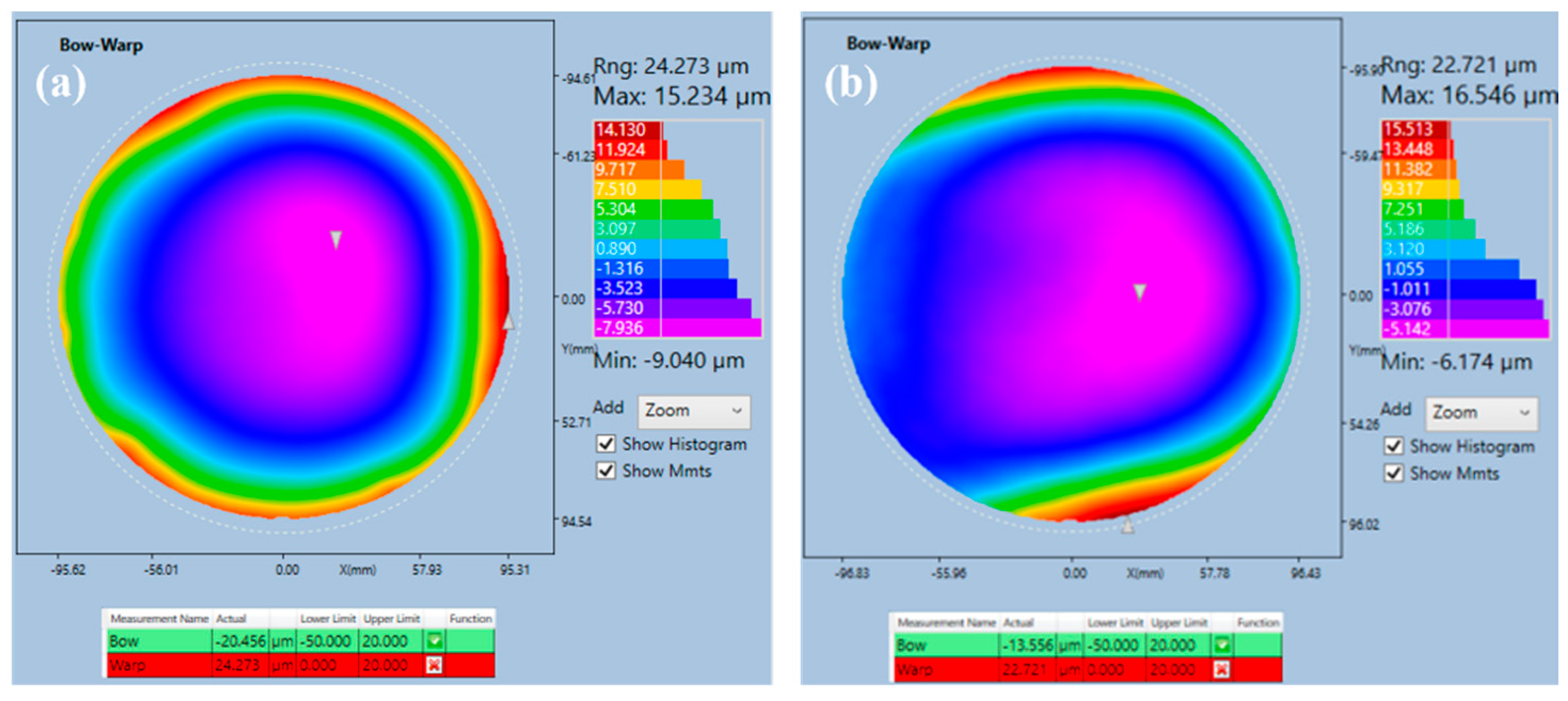
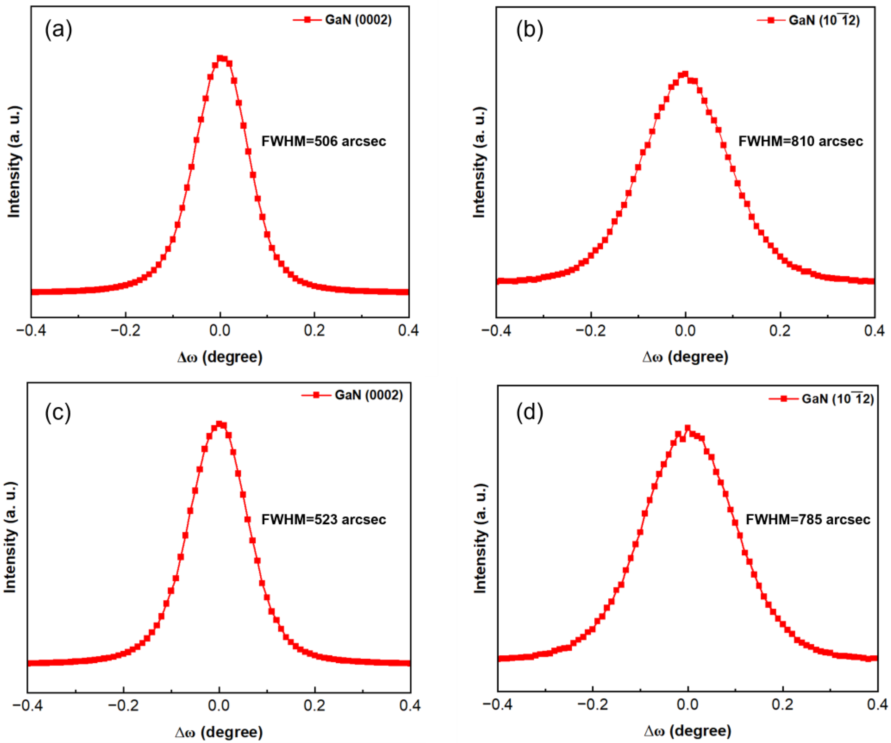
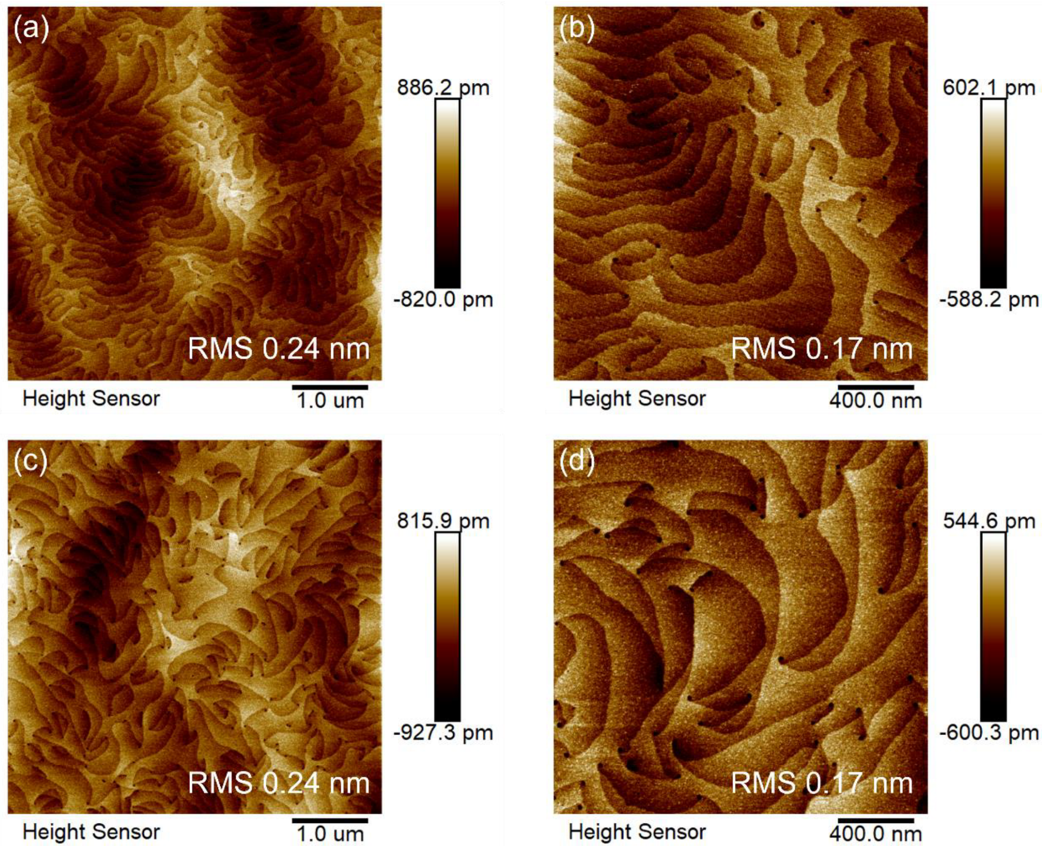
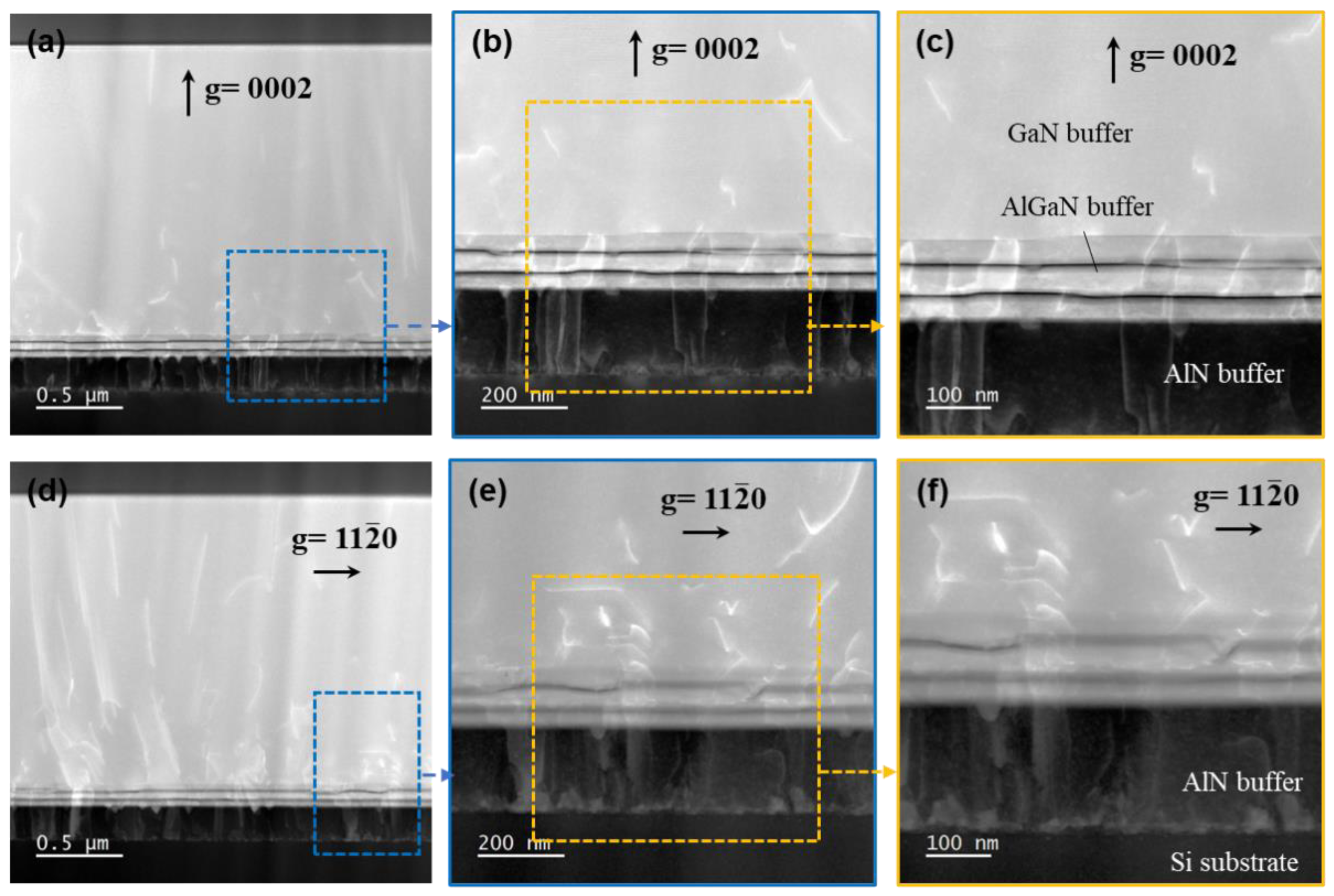
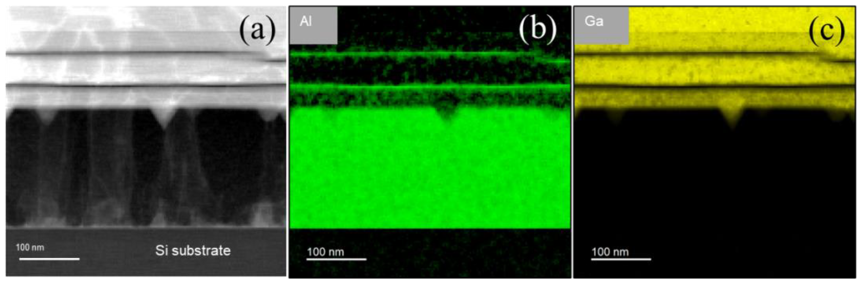
Using a metal–organic chemical vapor deposition (MOCVD) system, AlGaN/GaN HEMT epi-wafers were grown on 6- and 8-inch high-resistance Si(111) substrates with AIXTRON’s AIX G5+ equipment. Trimethylgallium (TMGa), trimetahylaluminum (TMAl), and ammonia (NH3) were used as precursors for Ga, Al, and N, respectively. TMAl was pre-flowed at 950 °C for 10 s on the Si(111) substrate, followed by the growth of 200 nm thick high-temperature (HT) AlN at 1100 °C. After the HT-AlN growth, AlxGa1−xN buffer layers were grown at a temperature above 1000 °C. And a 50 nm thick unintentionally doped GaN layer as a nucleation layer and a 1.8 μm thick C-doped GaN layer were grown at 1050 °C. Subsequently, a 200 nm thick GaN channel layer was grown at 1150 °C, and a 0.8 nm AlN spacer layer and an 18 nm thick AlGaN barrier with an Al composition of 25% were grown at 1200 °C. Finally, a 2 nm thick GaN cap layer was grown at 1150 °C, as illustrated in Figure 1. The enlarged image in Figure 1 shows that the 150 nm AlGaN buffer layer exhibited a specific structural design similar to a two-layer sandwich structure.
The crystal quality of the epi-layers was evaluated by high-resolution X-ray diffraction (HR-XRD), and the warp was measured by a flatness measurement system. Atomic force microscopy (AFM) in tapping mode was used to examine the surface morphology of the wafers. The transport properties of the AlGaN/GaN heterostructures were evaluated using Hall measurements. Scanning transmission electron microscopy (STEM) was used to obtain cross-sectional annular dark field (ADF) images to characterize the different types of dislocations. Additionally, electron energy-loss spectroscopy (EELS) was employed to analyze the elemental content and distribution within the AlN nucleation layer as well as the AlGaN buffer layer. Cross-sectional TEM samples were prepared with a zeiss 550 FIB/SEM with a final thinning voltage of 2 kV. A JEOL GRAND ARM300 microscope system operated at 300 kV was used to acquire cross-sectional TEM and STEM images.
Figure 2 shows typical bow–warp images of 6- and 8-inch AlGaN/GaN HEMT epi-wafers. Both the 6- and 8-inch epi-wafers exhibited a warp of less than 30 μm, indicating a high level of stress control, which ensures the high quality of epi-wafers and also enables devices to perform precisely and stably. It is worth noting that the 8-inch epi-wafers exhibited a superior stress control capacity, but their flatness symmetry was slightly inferior to that of the 6-inch epi-wafers. There were slight differences in warp and symmetry between the 6- and 8-inch epi-wafers, which were due to the fact that the tuning process of MOCVD is based on 8-inch epitaxial wafers.
The crystal quality of the epi-layers was assessed via full width at half maximum (FWHM) measurement of the rocking curves using HR-XRD, as shown in Figure 3. For the GaN epi-layers on the (0001) c-plane, the FWHM measurements of the rocking curves on the (0002) and (10 1 ¯ 2) planes were used to assess the c-type and a-type dislocation densities, respectively. As a result, there was almost no difference in crystal quality between the 6- and 8-inch epi-wafers due to the identical growth conditions and the buffer-layer structure. This phenomenon demonstrates the compatibility of thin AlGaN buffer layers at 6- and 8-inch wafer scales.
The detailed surface morphologies of the 6- and 8-inch AlGaN/GaN HEMT epi-wafers are presented in Figure 4. Distinct step-flow morphologies are clearly visible on the GaN surfaces of both the 6- and 8-inch epi-wafers, which indicate excellent crystal quality. Figure 4a,b reveal that the surface morphology of the 6-inch epi-wafer was smooth, with a root mean square roughness (RMS) of 0.24 nm. The 8-inch epi-wafer also exhibited excellent surface flatness, with an RMS of 0.24 nm (see Figure 4c,d). The black spots in the AFM image were caused by threading dislocations extending to the surface. The scarcity of black spots on the 6- and 8-inch epi-wafers indicates a low density of threading dislocations.
We evaluated the electrical characteristics of the 6- and 8-inch AlGaN/GaN HEMT epi-wafers by Hall measurement. The results show that the sheet resistance (Rsheet) ranged from 320 to 370 Ω sq−1 and that the electron mobility (μ) ranged from 1800 to 2010 cm2 V−1 s−1, while the two-dimensional electron gas density (ns) ranged from 0.8 to 1.1 × 1013 cm−2. Obviously, the AlGaN/GaN HEMT epi-wafers with a 100 nm thick AlGaN buffer layer exhibit excellent transport performance.
To further investigate the dislocation evolution characteristics of the epi-wafers and the interface properties of the multilayer films, cross-sectional annular dark-field STEM (ADF-STEM) was carried out. Due to the consistent buffer-layer structure and similar STEM results for the 6- and 8-inch epi-wafers, we will no longer specifically note the sizes of epi-wafers. As shown in Figure 5, the ADF-STEM images were obtained at the same position with different diffraction vectors. Figure 5a shows c-type (Burgers vector b = <0001>) and (a+c)-type (Burger vector b = 1 3 <11 2 ¯ 3>) dislocations in Group III nitrides under the conditions of g = 0002. Figure 5c illustrates a-type (Burgers vector b = 1 3 <11 2 ¯ 0>) and (a+c)-type dislocations under the conditions of g = 11 2 ¯ 0. Thus, GaN layers mainly include a-type and (a+c)-type threading dislocations, with a small number of pure c-type dislocations. As evidenced from the figures, significant annihilation of threading dislocations occurs within the AlN nucleation layer, the thin AlGaN buffer layer, and the initial 200–300 nm thickness range of the GaN buffer layer.
Cross-sectional ADF-STEM images collected under the condition of g = 0002 (Figure 6a–c) demonstrate that the heterointerface plays an important role in reducing the number of c-type dislocations. In the AlGaN buffer layer, there are distinct traces of c-type dislocations moving along the interface between the 2 nm AlN and 2 nm Al0.53Ga0.47N insertion layers, promoting the approach and annihilation of adjacent c-type dislocations with opposite signs. In contrast to the c-type dislocations, the heterointerface appears to have little impact in terms of altering the movement direction of a-type dislocations, as evidenced by the cross-sectional ADF-STEM images (Figure 6d–f), which were collected under the condition of g = 11 2 ¯ 0. However, within the initial 200 to 300 nm thickness range of the GaN buffer layer, a significant amount of annihilation occurred via a-type dislocations. This was likely due to the combined effect of the faster lateral growth rate of GaN compared to AlN and AlGaN, as well as the rapid stress relaxation.
The ABF-STEM and BF-TEM images in Figure 7 clearly reveal the evolution of V-shaped pits in the AlN nucleation layer and the AlGaN buffer layer. These V-shaped pits likely form during the merging of AlN islands, often with one or multiple dislocations at their bottoms. During the growth of the AlN nucleation layer, the low surface mobility of Al atoms is unfavorable for the healing of these V-shaped pits. However, when switching to the growth of the Al0.18Ga0.82N layer with a lower Al content, the significantly high surface mobility of Ga atoms greatly enhances the lateral growth capability of the film, resulting in rapid filling in of the V-shaped pits.
The element composition and distribution of the AlN nucleation layer and the AlGaN buffer layer were characterized by EELS, and the distribution of Al and Ga elements is shown in Figure 8b,c. It can be seen that the content of Ga elements in the V-shaped pits is higher, which is consistent with the previous analysis. This also proves that the high surface mobility is key for Ga atoms’ filling in of the V-shaped pits.

3. Conclusions

In this work, we investigated the effect of a thin AlGaN buffer layer with a “sandwich” structure on the dislocation evolution of AlGaN/GaN HEMTs grown on 6- and 8-inch Si(111) substrates and evaluated its comprehensive performance. The thin AlGaN buffer layer with a “sandwich structure” showed excellent stress control capacity with a warpage degree lower than 30 μm. Moreover, comprehensive evaluations were conducted through XRD rocking curve, AFM, and Hall measurements, which demonstrated that the 6- and 8-inch AlGaN/GaN HEMT epi-wafers exhibit fine crystal quality and excellent electrical performance.
Notably, the dislocation evolution in the AlGaN buffer layer and the GaN epi-layer was characterized by STEM. The heterointerfaces within the buffer layer showed a significant effect on the lateral movement and annihilation of c-type dislocations, while they exerted a minor impact on a-type dislocations. The annihilation of a-type dislocations primarily occurred within the initial 200–300 nm range of the GaN buffer layer due to the collective effect of both the rapid lateral growth rate of GaN and stress relaxation. In addition, the evolution of V-shaped pits revealed by STEM suggests the critical role of the high surface mobility of Ga atoms in filling these pits, which was further confirmed by EELS. The investigation of dislocation evolution in the thin AlGaN buffer layer provides vital guidance for optimizing the performance and crystal quality of AlGaN/GaN HEMT epi-wafers grown on Si substrates and promises to enlarge their application scope in the electronic information era.

Author Contributions

Conceptualization, methodology, formal analysis, and preparation of the original draft were carried out by Y.Y. and J.H. was responsible for validation, data curation, writing—review and editing, methodology, and supervision. L.P. handled the epitaxial growth aspect, while B.M. and Q.W. conducted the characterization and analysis. B.Y. oversaw the project administration. All authors have read and agreed to the published version of the manuscript.

Funding

This work was supported by the Central Funds Guiding the Local Science and Technology Development Project of Hubei Province, China (grant no. 2022BFE001).

Data Availability Statement

The datasets generated and supporting the findings of this article are obtainable from the corresponding author upon reasonable request.

Conflicts of Interest

The authors declare no conflicts of interest.

References

  1. Wu, N.T.; Xing, Z.H.; Li, S.J.; Luo, L.; Zeng, F.Y.; Li, G.Q. GaN-based power high-electron-mobility transistors on Si substrates: From materials to devices. Semicond. Sci. Technol. 2023, 38, 063002. [Google Scholar] [CrossRef]
  2. Zhong, Y.; Zhang, J.; Wu, S.; Jia, L.; Yang, X.; Liu, Y.; Zhang, Y.; Sun, Q. A review on the GaN-on-Si power electronic devices. Fundam. Res. 2022, 2, 462–475. [Google Scholar] [CrossRef] [PubMed]
  3. Haziq, M.; Falina, S.; Manaf, A.A.; Kawarada, H.; Syamsul, M. Challenges and Opportunities for High-Power and High-Frequency AlGaN/GaN High-Electron-Mobility Transistor (HEMT) Applications: A Review. Micromachines 2022, 13, 2133. [Google Scholar] [CrossRef] [PubMed]
  4. Ajayan, J.; Nirmal, D.; Mohankumar, P.; Mounika, B.; Bhattacharya, S.; Tayal, S.; Fletcher, A.S.A. Challenges in material processing and reliability issues in AlGaN/GaN HEMTs on silicon wafers for future RF power electronics & switching applications: A critical review. Mater. Sci. Semicond. Process. 2022, 151, 106982. [Google Scholar] [CrossRef]
  5. Hsu, L.H.; Lai, Y.Y.; Tu, P.T.; Langpoklakpam, C.; Chang, Y.T.; Huang, Y.W.; Lee, W.C.; Tzou, A.J.; Cheng, Y.J.; Lin, C.H.; et al. Development of GaN HEMTs Fabricated on Silicon, Silicon-on-Insulator, and Engineered Substrates and the Heterogeneous Integration. Micromachines 2021, 12, 1159. [Google Scholar] [CrossRef] [PubMed]
  6. Li, L.; Nomoto, K.; Pan, M.; Li, W.S.; Hickman, A.; Miller, J.; Lee, K.; Hu, Z.Y.; Bader, S.J.; Lee, S.M.; et al. GaN HEMTs on Si with Regrown Contacts and Cutoff/Maximum Oscillation Frequencies of 250/204 GHz. IEEE Electron. Device Lett. 2020, 41, 689–692. [Google Scholar] [CrossRef]
  7. Teo, K.H.; Zhang, Y.H.; Chowdhury, N.; Rakheja, S.; Ma, R.; Xie, Q.Y.; Yagyu, E.; Yamanaka, K.; Li, K.X.; Palacios, T. Emerging GaN technologies for power, RF, digital, and quantum computing applications: Recent advances and prospects. J. Appl. Phys. 2021, 130, 160902. [Google Scholar] [CrossRef]
  8. Lai, Y.J.; Liu, Y.C.; Hsu, Y.F.; Wu, M.C. Characteristics Comparison of Nanochannel GaN-on-Si and GaN-on-SiC HEMTs. ECS J. Solid State Sci. Technol. 2023, 12, 075002. [Google Scholar] [CrossRef]
  9. Zhang, H.; Sun, Y.; Song, K.; Xing, C.; Yang, L.; Wang, D.; Yu, H.; Xiang, X.; Gao, N.; Xu, G.; et al. Demonstration of AlGaN/GaN HEMTs on vicinal sapphire substrates with large misoriented angles. Appl. Phys. Lett. 2021, 119, 072104. [Google Scholar] [CrossRef]
  10. Yeh, P.C.; Tu, P.T.; Liu, H.H.; Hsu, C.H.; Yang, H.Y.; Fu, Y.K.; Lee, L.H.; Tzeng, P.J.; Wu, Y.R.; Sheu, S.S.; et al. CMOS-compatible GaN HEMT on 200 mm Si-substrate for RF application. In Proceedings of the International Symposium on VLSI Technology, Systems and Applications (VLSI-TSA), Hsinchu, Taiwan, 19–22 April 2021. [Google Scholar]
  11. Xie, H.L.; Liu, Z.H.; Gao, Y.; Ranjan, K.; Lee, K.E.; Ng, G.I. CMOS-compatible GaN-on-Si HEMTs with cut-off frequency of 210 GHz and high Johnson’s figure-of-merit of 8.8 THz V. Appl. Phys. Express 2020, 13, 026503. [Google Scholar] [CrossRef]
  12. Peralagu, U.; Alian, A.; Putcha, V.; Khaled, A.; Rodriguez, R.; Sibaja-Hernandez, A.; Chang, S.; Simoen, E.; Zhao, S.E.; Jaeger, B.D.; et al. CMOS-compatible GaN-based devices on 200 mm-Si for RF applications: Integration and Performance. In Proceedings of the 2019 IEEE International Electron Devices Meeting (IEDM), San Francisco, CA, USA, 7–11 December 2019; pp. 17.12.11–17.12.14. [Google Scholar]
  13. Zhang, L.; Hong Lee, K.; Riko, I.M.; Huang, C.-C.; Kadir, A.; Lee, K.E.; Jin Chua, S.; Fitzgerald, E.A. MOCVD growth of GaN on SEMI-spec 200 mm Si. Semicond. Sci. Technol. 2017, 32, 065001. [Google Scholar] [CrossRef]
  14. Cheng, J.P.; Yang, X.L.; Sang, L.; Guo, L.; Hu, A.Q.; Xu, F.J.; Tang, N.; Wang, X.Q.; Shen, B. High mobility AlGaN/GaN heterostructures grown on Si substrates using a large lattice-mismatch induced stress control technology. Appl. Phys. Lett. 2015, 106, 142106. [Google Scholar] [CrossRef]
  15. Su, J.; Armour, E.A.; Krishnan, B.; Lee, S.M.; Papasouliotis, G.D. Stress engineering with AlN/GaN superlattices for epitaxial GaN on 200 mm silicon substrates using a single wafer rotating disk MOCVD reactor. J. Mater. Res. 2015, 30, 2846–2858. [Google Scholar] [CrossRef]
  16. Meneghini, M.; De Santi, C.; Abid, I.; Buffolo, M.; Cioni, M.; Khadar, R.A.; Nela, L.; Zagni, N.; Chini, A.; Medjdoub, F.; et al. GaN-based power devices: Physics, reliability, and perspectives. J. Appl. Phys. 2021, 130, 181101. [Google Scholar] [CrossRef]
  17. Zhang, Y.; Dadgar, A.; Palacios, T. Gallium nitride vertical power devices on foreign substrates: A review and outlook. J. Phys. D Appl. Phys. 2018, 51, 273001. [Google Scholar] [CrossRef]
  18. Feng, M.X.; Liu, J.X.; Sun, Q.; Yang, H. III-nitride semiconductor lasers grown on Si. Prog. Quantum Electron. 2021, 77, 100323. [Google Scholar] [CrossRef]
  19. Zhan, X.; Liu, J.; Sun, X.; Huang, Y.; Gao, H.; Zhou, Y.; Li, Q.; Sun, Q.; Yang, H. Crack-free 2.2 μm-thick GaN grown on Si with a single-layer AlN buffer for RF device applications. J. Phys. D Appl. Phys. 2023, 56, 015104. [Google Scholar] [CrossRef]
  20. Lee, J.H.; Im, K.S. Growth of High Quality GaN on Si (111) Substrate by Using Two-Step Growth Method for Vertical Power Devices Application. Crystals 2021, 11, 234. [Google Scholar] [CrossRef]
  21. He, X.; Feng, Y.; Yang, X.; Wu, S.; Cai, Z.; Wei, J.; Shen, J.; Huang, H.; Liu, D.; Chen, Z.; et al. Step-Graded AlGaN vs superlattice: Role of strain relief layer in dynamic on-resistance degradation. Appl. Phys. Express 2021, 15, 011001. [Google Scholar] [CrossRef]
  22. Umeda, H. GaN on Si: Epitaxy and Devices. In Wide Bandgap Semiconductors for Power Electronics; Wiley: Hoboken, NJ, USA, 2021; pp. 555–582. [Google Scholar] [CrossRef]
  23. Kim, J.G.; Cho, C.; Kim, E.; Hwang, J.S.; Park, K.H.; Lee, J.H. High Breakdown Voltage and Low-Current Dispersion in AlGaN/GaN HEMTs with High-Quality AlN Buffer Layer. IEEE Trans. Electron Devices 2021, 68, 1513–1517. [Google Scholar] [CrossRef]
  24. Wang, K.; Li, M.; Yang, Z.; Wu, J.; Yu, T. Stress control and dislocation reduction in the initial growth of GaN on Si (111) substrates by using a thin GaN transition layer. CrystEngComm 2019, 21, 4792–4797. [Google Scholar] [CrossRef]
  25. Zhang, Z.-Z.; Yang, J.; Zhao, D.-G.; Liang, F.; Chen, P.; Liu, Z.-S. Influence of the lattice parameter of the AlN buffer layer on the stress state of GaN film grown on (111) Si. Chin. Phys. B 2023, 32, 028101. [Google Scholar] [CrossRef]
  26. Zhang, J.; Yang, X.L.; Feng, Y.X.; Li, Y.; Wang, M.J.; Shen, J.F.; Wei, L.; Liu, D.S.; Wu, S.; Cai, Z.D.; et al. Vacancy-engineering-induced dislocation inclination in III-nitrides on Si substrates. Phys. Rev. Mater. 2020, 4, 073402. [Google Scholar] [CrossRef]
  27. Besendörfer, S.; Meissner, E.; Lesnik, A.; Friedrich, J.; Dadgar, A.; Erlbacher, T. Methodology for the investigation of threading dislocations as a source of vertical leakage in AlGaN/GaN-HEMT heterostructures for power devices. J. Appl. Phys. 2019, 125, 095704. [Google Scholar] [CrossRef]
  28. Sasangka, W.A.; Syaranamual, G.J.; Made, R.I.; Thompson, C.V.; Gan, C.L. Threading dislocation movement in AlGaN/GaN-on-Si high electron mobility transistors under high temperature reverse bias stressing. Aip Adv. 2016, 6, 095102. [Google Scholar] [CrossRef]
  29. Liu, J.X.; Huang, Y.N.; Sun, X.J.; Zhan, X.N.; Sun, Q.; Gao, H.W.; Feng, M.X.; Zhou, Y.; Ikeda, M.; Yang, H. Wafer-scale crack-free 10 mu m-thick GaN with a dislocation density of 5.8 × 107 cm−2 grown on Si. J. Phys. D-Appl. Phys. 2019, 52, 425102. [Google Scholar] [CrossRef]
  30. Zhang, J.; Yang, X.; Ma, H.; Zhang, Q.; Shen, B. Effects of Al doping on dislocation inclinations and strain of GaN films on Si substrates. AIP Adv. 2023, 13, 025250. [Google Scholar] [CrossRef]
Figure 1. Schematic diagram of the AlGaN/GaN HEMT structure with a thin AlGaN buffer layer.
Inorganics 12 00207 g001
Figure 2. Bow-warp images of AlGaN/GaN HEMTs on Si epi-wafers: (a) 6-inch; (b) 8-inch.
Inorganics 12 00207 g002
Figure 3. The XRD rocking curves of AlGaN/GaN HEMTs on Si epi-wafers: (a) the (0002) plane and (b) the (10 1 ¯ 2) plane of the 6-inch epi-wafer; (c) the (0002) plane and (d) the (10 1 ¯ 2) plane of the 8-inch epi-wafer.
Inorganics 12 00207 g003
Figure 4. AFM images of AlGaN/GaN HEMTs on Si epi-wafers with areas of (a) 5 × 5 μm2 and (b) 2 × 2 μm2 for the 6-inch epi-wafer and (c) 5 × 5 μm2 and (d) 2 × 2 μm2 for the 8-inch epi-wafer.
Inorganics 12 00207 g004
Figure 5. Cross-sectional ADF-STEM images of the 6-inch AlGaN/GaN HEMT epi-wafer: (a) under the condition of g = 0002; (b) magnified view of (a); (c) under the condition of g = 11 2 ¯ 0; (d) magnified view of (c).
Inorganics 12 00207 g005
Figure 6. Cross-sectional ADF-STEM images of the 8-inch AlGaN/GaN HEMT epi-wafer: (a) g = 0002; (b) partial enlargement of figure (a); (c) partial enlargement of figure (b); (d) g = 11 2 ¯ 0; (e) partial enlargement of figure (d); (f) partial enlargement of figure (d).
Inorganics 12 00207 g006
Figure 7. Cross-sectional STEM and TEM images of the AlN nucleation layer and the AlGaN buffer layer: (a) ABF-STEM image; (b) BF-TEM image.
Inorganics 12 00207 g007
Figure 8. STEM and EELS characterizations of the buffer layer: (a) ADF-STEM image; (b) STEM-EELS mapping of Al elements; (c) STEM-EELS mapping of Ga elements.
Inorganics 12 00207 g008
Disclaimer/Publisher’s Note: The statements, opinions and data contained in all publications are solely those of the individual author(s) and contributor(s) and not of MDPI and/or the editor(s). MDPI and/or the editor(s) disclaim responsibility for any injury to people or property resulting from any ideas, methods, instructions or products referred to in the content.

