Abstract
This study explores a novel approach to surface-enhanced Raman scattering (SERS) substrate fabrication through the heat-induced fragmentation of gold nanowires (Au NWs) and its impact on gold nanoparticle adhesion/static friction using atomic force microscopy manipulations. Controlled heating experiments and scanning electron microscopy measurements reveal significant structural transformations, with NWs transitioning into nanospheres or nanorods in a patterned fashion at elevated temperatures. These morphological changes lead to enhanced Raman signals, particularly demonstrated in the case of Rhodamine B molecules. The results underscore the critical role of NW shape modifications in augmenting the SERS effect, shedding light on a cost-effective and reliable method for producing SERS substrates.
1. Introduction
Surface-enhanced Raman scattering (SERS) is one of the most promising analytical techniques to have emerged over the years as laser technology, nanophotonics, and plasmonics have advanced [1]. It is a method for enhancing the electromagnetic field on the surface of noble-metal nanostructures or nanogaps by combining Raman spectroscopy with the localised surface plasmon resonance effect [2,3,4]. In general, it addresses the limitation of the weak Raman scattering of molecules, effectively amplifying the subtle Raman signals [4,5].
Gold nanoparticles (Au NPs) have become increasingly popular in the area of SERS applications [6,7,8]—they are known for their exceptional chemical stability in diverse environments, including high temperatures and pressures, and they are versatile tools in SERS measurements; they are easily fabricated with applications in various fields [9], from sensing [10] to drug delivery [11]. Au NPs are able to improve the Raman scattering efficiency by several orders of magnitude [12]. Their suitability for the highly sensitive detection of minute amounts of molecules makes Au NPs an ideal choice, and their cost-effectiveness in enhancing Raman scattering makes them attractive for a variety of applications [13,14].
The development and production of substrates with the best-enhancing properties, as well as the structural characteristics of SERS substrates, are currently active research fields [15,16]. The size, shape, interparticle distance, and general arrangement of the NPs, as well as the wavelength of the excitation source, all affect a substrate’s SERS enhancement factor (EF) [17]. Earlier investigations have demonstrated a correlation between the interparticle distance and the degree of SERS enhancement [16]. This relationship can be attributed to the increase in specific surface coverage of the particles’ active surfaces as they come closer to one another. Furthermore, the surface density of so-called hot spots, representing areas with amplified near-field intensities resulting from coupled plasmons between the particles, also increases with decreasing interparticle distance. These collective effects contribute to the improved efficiency of SERS. As a result, controlling and optimizing the interparticle distance represents a crucial aspect in enhancing SERS performance for a variety of applications [18].
SERS substrates tend to suffer from drawbacks such as limited reproducibility and disorderly arrangement, which hinder the widespread use of SERS. Consequently, it is important to develop SERS active substrates that are both consistent and well organized [19]. In order to prevent the dispersion of random hot spots, metallic nanostructures must have a high degree of homogeneity in their morphology (size and shape) [20]. Thus, one of the main challenges is to create a repeatable particle arrangement. Some studies have suggested that spherical Au and silver NPs with a diameter of 50 nm exhibit the highest SERS EFs [21,22], while others have indicated a broader optimal range, spanning from 30 nm to 100 nm, for enhanced SERS signals [23,24].
According to Bell et al. [25], SERS substrates can be roughly categorized into three groups: (1) nanostructures created using lithographic techniques, where the metal is deposited on the substrate using top-down approaches; (2) NPs constructed on surfaces using a bottom-up approach; and (3) NPs in suspension. Lithography methods can provide SERS substrates with the most regular structures, but scaling up their lithographic manufacture is challenging, which drives up the cost. Thus, categories (2) and (3) of materials are less expensive and simpler to create, making them more likely candidates for the in-field use of SERS, particularly as a low-cost point-of-care diagnostic tool [26]. Despite the advantages, NPs constructed on surfaces can pose a challenge: the potential displacement of metal NPs during the drop-casting process of the test material.
It is well known that the adhesion and static friction of metal nanostructures decrease significantly after annealing due to the rounding and decreasing of the contact area with the substrate [27]. The atomic force microscopy (AFM) manipulation approach can be successfully applied to probe the adhesion/static friction magnitude and to estimate the fraction of movable NPs [28], which, for example, can be displaced or washed away during the drop-casting of the investigated chemical solution due to capillary forces. This understanding becomes critical when examining techniques like heat-induced nanowire (NW) fragmentation, which could potentially be used for creating SERS substrates. In this method, NWs are made through chemical synthesis, followed by thermal annealing to induce fragmentation to arrange the NWs into spheres. The melting temperature of NPs is commonly understood to decrease with their size, occurring at significantly lower temperatures than bulk materials [29]. Considerations such as surface diffusion and Rayleigh instability [30] have revealed that Au nanostructures can fuse and break apart at temperatures as low as 200 °C. As a result, it would be possible to easily build the substrates and have control over their layout and dimensions.
In this article, we evaluated the feasibility of heat-induced Au NW fragmentation for the production of cost-effective and reliable SERS-active substrates, and we compared the SERS enhancement for untreated and thermally annealed Au NPs. We also investigated the effect of temperature on the formation of Au NW fragments, as well as the adhesive behaviour of NPs produced with this approach.
2. Materials and Methods
2.1. Materials
Experiments were conducted on 12 × 12 mm (100) two-side polished silicon p-type (boron-doped) substrates (MicroChemicals GmbH, Ulm, Germany) with 500 ± 15 µm thicknesses. Si wafers were oxidized at 1000 °C for 45 min in a laboratory furnace to grow a silicon oxide surface layer, preventing eutectic alloy formation between Si substrate and Au NWs during further heating.
Au NPs were produced from Au seeds in a three-step synthesis process adopted from Kim et al. [31]. All chemicals were purchased from Sigma-Aldrich (Darmstadt, Germany). The seed solution was prepared in a 25 mL glass bottle by mixing 19.8 mL of 0.025 M sodium citrate solution in deionized (DI) water and 0.2 mL of 0.00025 M HAuCl4 solution. Ice-cold 0.01 M NaBH4 solution was separately prepared. A volume of 0.6 mL of the NaBH4 solution was added into the sodium citrate solution while stirring vigorously. The solution immediately turned orange-red. The growth solution was prepared by mixing in 240 mL DI water with 0.2 M hexadecyltrimethylammonium bromide (CTAB) and 10 mL of 0.0001 M of HAuCl4. Afterwards, 1.5 mL of 0.1 M ascorbic acid was added. The growth solution was divided into two 25 mL glass bottles labelled “A” and “B”, and 200 mL was placed in vessel “C” (flat-bottom conical flask). Into vessel “C”, 0.25 mL of concentrated HNO3 was added. A volume of 0.2 mL of the citrate stabilized Au seed NPs solution was added into a bottle labelled “A” and stirred for 1 min. Then, 0.2 mL of solution from bottle “A” was transferred to bottle “B” and stirred for 1 min. Lastly, 0.2 mL of solution in bottle “B” was then transferred to vessel “C” and stirred. The “C” solution was kept at a 25 °C temperature for 12 h (note that if the solution temperature drops below 25 °C, unwanted crystallization of CTAB starts). The precipitates of Au NPs were observed on the bottom of the vessel after the reaction. The supernatant was poured out of the solution, and the Au NWs precipitate was redispersed in 5 mL of DI water. Synthesised NWs were a few μm long and with a diameter of ~50 nm. Shorter nanostructures, nanorods (NRs), were about 60–100 nm long with a diameter of ~18 nm.
2.2. Sample Preparation
The removal of surfactants from the Au NW solution was conducted according to a 5-cycle process. Each cycle consisted of 20 min of sonication followed by 20 min of centrifugation at 5000 rpm. For the sonication, distilled water was used as the solution. After centrifugation, the excess solution was removed and replaced with distilled water. The process was repeated 5 times in order to ensure the maximum removal of surfactants from the Au NW solution. The method involved applying a solution of Au NWs onto a Si substrate in the form of 5 droplets of 2.5 μL each, resulting in a film of Au NWs.
2.3. Annealing
Thermal behaviour of NWs was investigated through controlled heating processes in a SNOL 8.2/1100 (Snoltherm UAB, Narkūnai, Lithuania) laboratory furnace. Au NWs were subjected to two distinct heating schemes to comprehend their thermal behaviour and structural transformations. The first scheme employed gradual heating of the same NW sample at temperatures ranging from 300 °C to 600 °C in increments of 50 °C, with a consistent duration of 30 min at each temperature step. After each heating temperature, the sample was imaged with a scanning electron microscope (SEM). The second scheme involved rapid heating, in which a fresh sample was used for each experiment, enabling precise determination of the temperature at which fragmentation initiates. Heating was carried out at temperatures from 300 °C to 600 °C, each for a duration of 30 min.
2.4. Characterisation
SEM studies were performed on Helios 5 UX DualBeam (Thermo Fisher Scientific, Eindhoven, The Netherlands) at an acceleration voltage of 5 keV and a beam current of 25 pA. An examination of Au NWs was undertaken, encompassing the measurement of around 90 individual NPs, using the Fiji ImageJ2 software (version 2.9.0/1.53 t) [32]. The measurements were conducted using the Analyze-Measure function, with the selection of the NW dimensions based on the background contrast of SEM micrographs, allowing for accurate determination of the start and end points of each NP. For unprocessed SEM images of Au NRs and NWs, refer to Supplementary Materials Figures S1 and S2.
The NPs’ manipulations were performed in an AFM (Dimension Edge, Bruker, Billerica, MA, USA) using a rectangular AFM cantilever (NCHR, Bruker, MA, USA) with a force constant of k = 42 and a resonance frequency of 320 kHz. The manipulation procedure is similar to that reported in Oras et al. [28], with a few modifications. All imaging and manipulation scans were performed in the tapping mode. First, an overview image of a 20 × 20 µm area was taken. Then, a series of manipulation scans were performed with a 10 × 10 µm scan range, increasing the force by which the tip is pushed to the surface by each scan. After manipulations, another overview image with a size of 20 × 20 µm was taken. By comparing the before and after images, the amount of movable and unmovable NPs was counted. Manipulation was performed in 5 different areas in total. To calculate the dissipated power, the formula developed by Anczykowski et al. [33] was used:
where k is the cantilever’s force constant, f0 is the cantilever’s resonance frequency, Aset is the setpoint amplitude, Apiezo is the driving amplitude, θ is the phase signal, and Q is the quality factor of the AFM cantilever. The phase signal was extracted from tapping mode phase images using the Gwyddion software (version 2.63).
P = k∙f0∙(Aset∙Apiezo∙sinθ − Aset2/Q),
Samples were examined with Raman spectroscopy before and after heating. Then, 5 μL of 6.1∙10−5 M Rhodamine B was applied by drop-casting. The Raman spectroscopy was performed using a Princeton Instruments TriVista CRS Confocal Raman Microscope (TR777) (S&I Spectroscopy & Imaging GmbH, Warstein, Germany). The instrument is equipped with three monochromators and a microscope, featuring diffraction gratings with varying line densities of 600, 900, and 1800 lines/mm and a focal length of 750 mm. The slit aperture of the microscope was set at F/9.8. For excitation, a Laser2000 diode laser with a wavelength of 785 nm was employed, providing a maximum output power of 200 mW. The laser that was used in measurements had a diameter of approximately 20 µm, implying that around 5–10 NWs were in the measurement area. A total of 5 spots from each sample were studied. Exposure times and laser power at the samples were matched for all measurements. The original intensities of the spectra were left in the relative units. Background extraction was performed using Origin software (version 9.8.0.200) by approximating the fluorescence spectrum with a spline and subtracting it from the total spectrum, in return giving the isolated Raman spectrum. The EFs for Rhodamine B molecules were calculated with respect to a pure Rhodamine B powder spectrum at the 1358 cm−1 peaks according to the equation [34]:
where ISERS is the Raman intensity and CSERS is the concentration of Rhodamine B used in SERS measurements; IRS is the Raman intensity, and CRS is the concentration of Rhodamine B used in routine Raman measurements.
3. Results
3.1. Au NP Characterisation
As-synthesised Au NWs and Au NRs were examined using SEM. By systematically measuring the width and length of both NWs and NRs, we aimed to gain insights into the physical characteristics and variability within the Au NWs and NRs. The collected data showed that the average length of the observed NRs (Figure 1a) was 83.5 nm, with a standard deviation (SD) of 9.4 nm, illustrating the range of length differences within the sample. Furthermore, the NRs demonstrated an average width of 18.4 nm, with a SD of 1.4 nm, indicating the degree of width variation. The average length of the observed NWs (Figure 1b) was determined to be 1.9 μm, with a SD of 0.7 μm. Additionally, the NWs exhibited an average width of 50.5 nm, with a SD of 5.5 nm. These findings highlight the relatively uniform length of the NWs while demonstrating a slightly higher variability in their width.
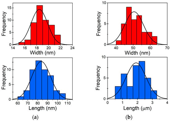
Figure 1.
Size distribution of as-prepared (a) Au NRs and (b) Au NWs.
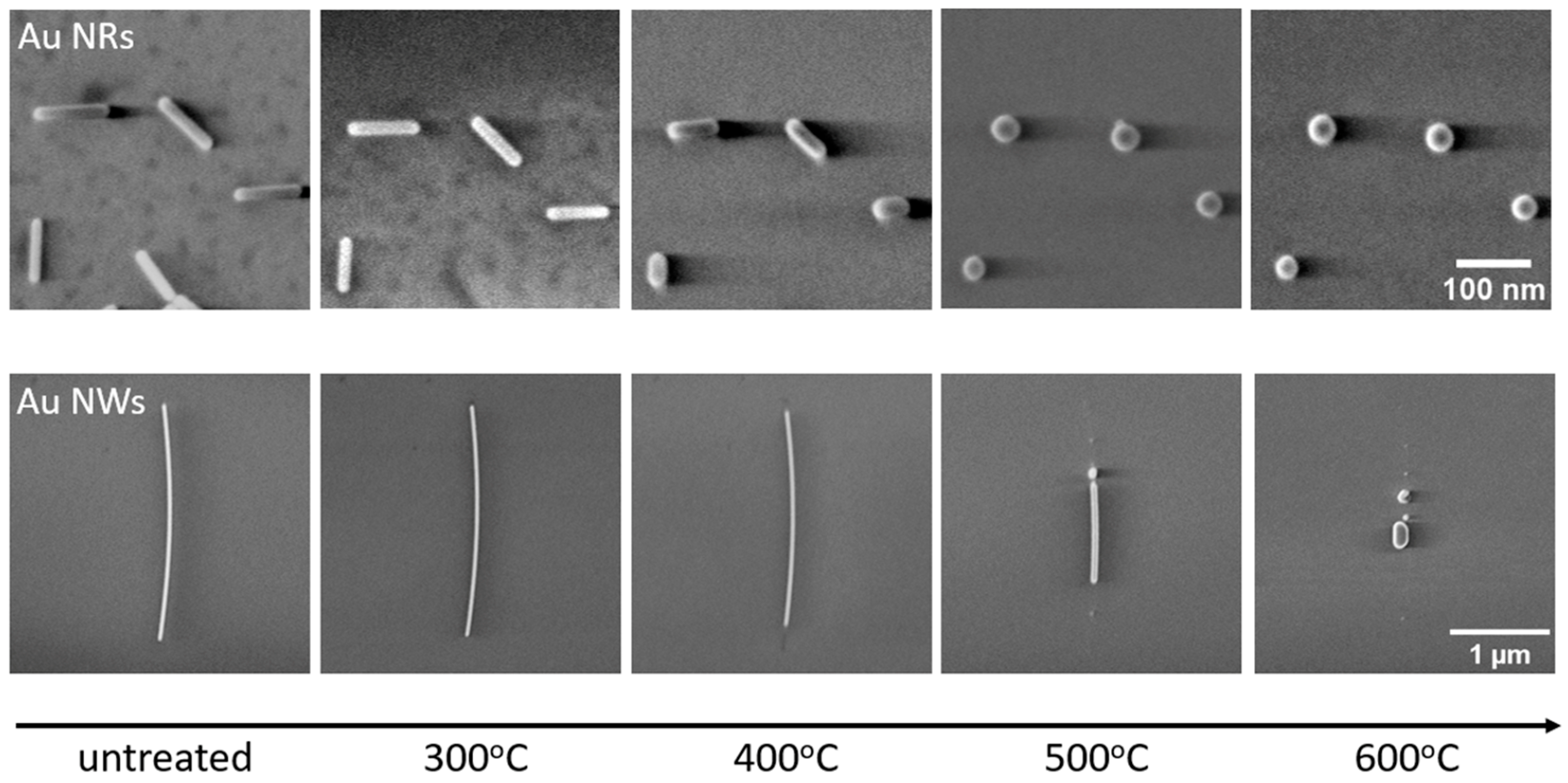
A controlled gradual heating procedure on the identical NW sample was implemented, elevating the temperature incrementally from 300 °C to 600 °C in 50 °C intervals and ensuring a constant duration of 30 min at each temperature step (the first heating scheme). In the SEM micrographs provided (Figure 2), it is evident that both the NRs and NWs exhibit a tendency to reduce in length and increase in width due to the diffusion of Au atoms. When the temperature is 400 °C, both types of nanostructures exhibit visible alterations in their morphology. The temperature range between 400 °C and 500 °C marks a period of remarkably swift transformations in both NRs and NWs.

Figure 2.
SEM micrographs of untreated and gradually thermally annealed (first heating scheme) Au NRs and NWs.
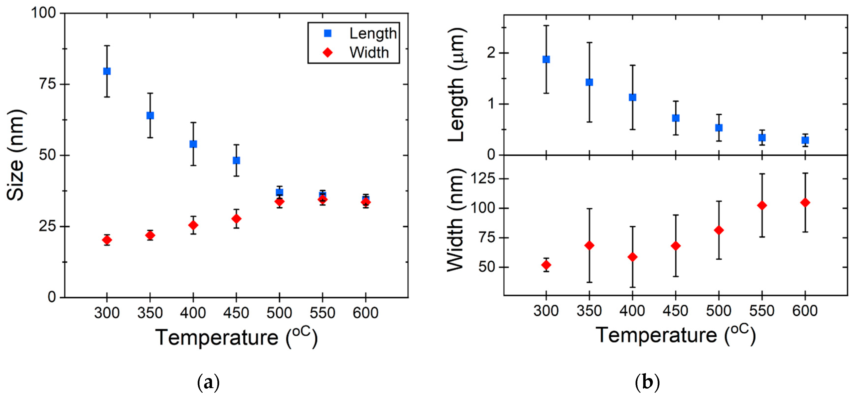
To establish statistical evidence, we systematically measured the dimensions of nanostructures after each heating cycle (the first heating scheme). Following the nanostructure measurements, it became evident that as the heating temperature gradually increased, the length of the structures decreased while the width increased. At around 550 °C, NRs (Figure 3a) demonstrated a propensity to transition into a thermodynamically more stable state, forming nanospheres. A similar phenomenon was observed with NWs (Figure 3b), where they were also inclined towards forming nanospheres under comparable conditions. NWs with a significant length-to-width ratio have a higher aspect ratio, meaning their length is much larger than their width. At low temperatures, all atoms are restricted to vibrational motion around their equilibrium positions, ensuring the NW retains its original structure and shape. When the temperature rises higher than 500 °C, the diffusive activities of atoms in the surface region become significant [35]. The rearrangement and diffusion of surface atoms into a spherical configuration are processes facilitated by the first heating scheme, allowing for sufficient time for these transformations to occur.
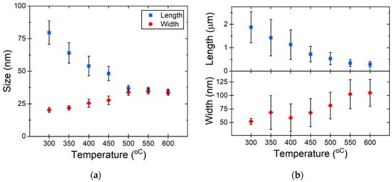
Figure 3.
Change in particle size depending on the heating temperature for (a) Au NRs and (b) Au NWs.
The second heating scheme was conducted to investigate the fragmentation behaviour of Au NWs under varying temperature conditions. The fragmentation of metal NWs at elevated temperatures into shorter pieces is a well-known phenomenon called Rayleigh instability [30]. This process is realised via surface atomic diffusion and is driven by surface energy minimization, where the resulting fragments tend to be faceted by {111} surfaces. The pentagonal Au wire surfaces were initially {100}, which transitioned into the more energetically favourable surfaces {111} at the wire ends. As a result, the NW broke up into several fragments or NRs. From previous experiments, it was visible that gradual heating gave more time for diffusion to induce a shape change, and the NWs tended to transform into nanosphere instead of fragmenting into several pieces. As illustrated in Figure 4, it becomes evident that if heated rapidly at 600 °C for 30 min via the second scheme, Au NWs are broken down into smaller fragments. As a result, NWs exhibit a periodicity in the spacing between these fragmented sections.

Figure 4.
SEM micrographs of rapidly heated (the second heating scheme) NWs at 600 °C for 30 min.
3.2. AFM Measurements
To explore the fabrication of robust SERS substrates, it is essential to ensure good adhesion of NPs to the substrate surface, preventing their displacement or washing away by dye-containing solutions. In this context, AFM manipulations were employed to examine whether the NPs, generated through the second heating scheme at 600 °C, achieved the required adhesion to the substrate. The mobility of the Au NPs was evaluated by means of the power dissipated in tapping-mode AFM, which has previously been shown to be an effective technique for the evaluation of NP mobility. The heat-induced rounding of NPs is expected to diminish the contact area, consequently lowering friction forces, aligning with the established relationship τ = F/A, where τ represents contact strength, F denotes friction force, and A signifies contact area [28]. In total, more than 400 Au NPs were subjected to measurement, and approximately 83.7% of these NPs exhibited no mobility under AFM manipulations. In Figure 5, the topography images reveal the changes in fragmented Au NWs on the Si substrate before (Figure 5a) and after (Figure 5b) AFM manipulations. These visuals highlight how the manipulations affect NP arrangement and adhesion. The median power dissipated for moving an NP was 0.13 pW. These findings emphasize the effectiveness of the proposed fabrication approach in creating stable SERS substrates with well-adhered NPs.
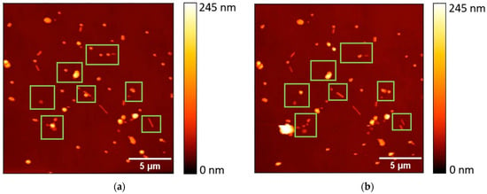
Figure 5.
A topography image of a 20 × 20 µm area of thermally annealed (600 °C) Au NWs on the Si substrate: (a) before AFM manipulations; (b) after AFM manipulations. The green frames mark the areas of NP displacement.
3.3. Raman Measurements
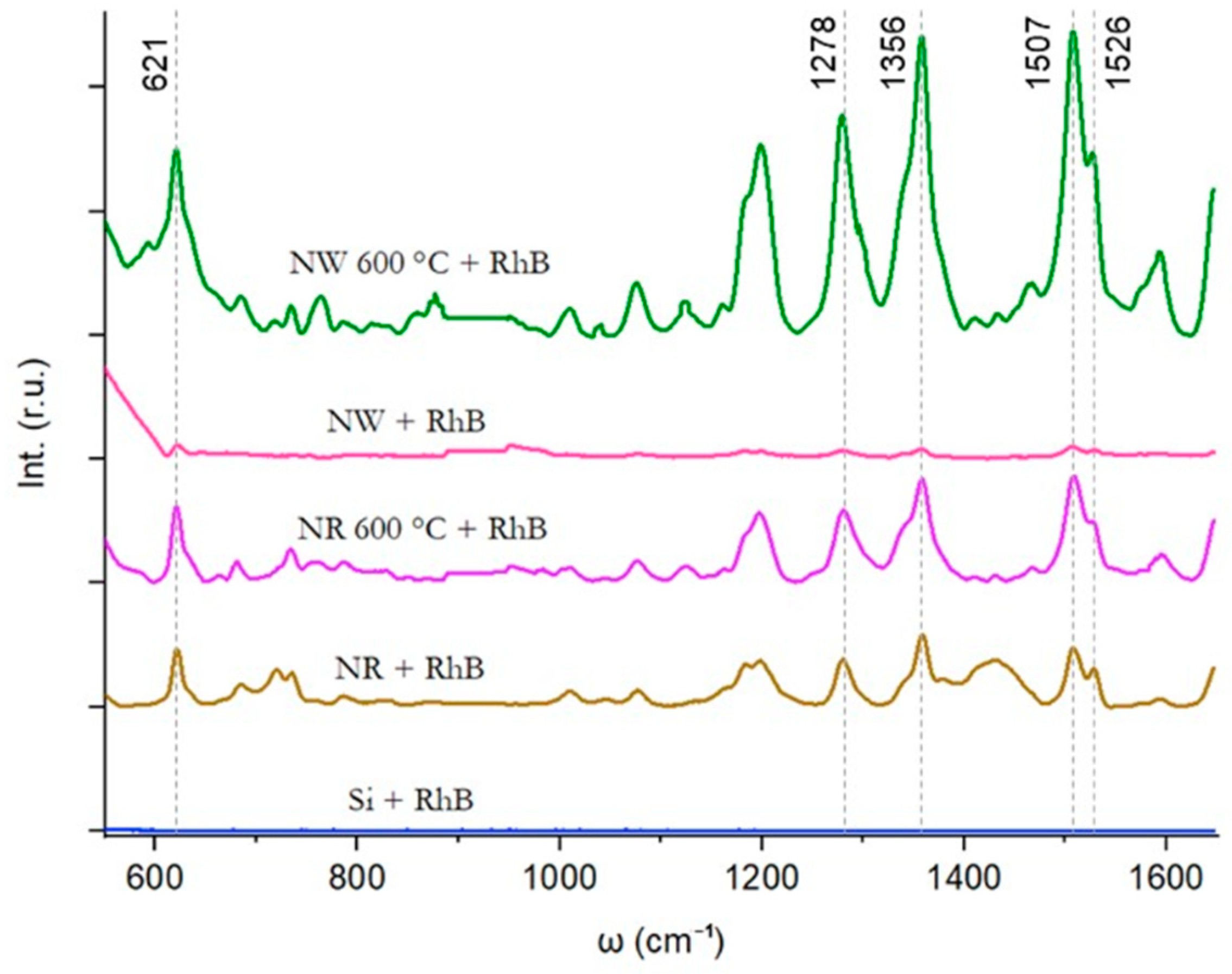
Raman measurements of Rhodamine B molecules adsorbed on a Si wafer surface with untreated and thermally treated Au nanostructures were investigated (Figure 6). Despite the excitation wavelength being optimized for Rhodamine B, no significant Raman peaks associated with Rhodamine B were detected on the bare Si wafer surface. To enhance the Raman signal of Rhodamine B, Au nanostructures before and after thermal annealing at 600 °C via the second heating scheme were introduced onto the Si wafer surface. For substrates with as-prepared Au NRs and NWs, the main SERS peaks of Rhodamine B at 621, 1278, 1356, 1507, and 1526 cm−1 [36] could be observed. Refer to Supplementary Materials Figure S3 for background Raman scattering data from each SERS substrate in the absence of Rhodamine B. Measurements for substrates with thermally annealed NRs and NWs resulted in an increased Raman signal for Rhodamine B, as evidenced by the amplified Raman peaks observed in the measured spectra. The Raman spectra of the heated NWs exhibited significantly higher intensities compared to the heated NRs. The calculated EFs highlight the substantial improvement achieved through annealing at 600 °C. Specifically, the EF for Au NRs is 3.8 × 10⁵, increasing to 8.3 × 10⁵ for Au NRs annealed at 600 °C. Additionally, the EF for annealed Au NWs is 1.6 × 10⁶, representing a nearly 30-fold increase compared to unannealed NWs with EF 5.5 × 10⁴.

Figure 6.
Raman scattering from Rhodamine B molecules on oxidised Si wafer with untreated and thermally treated Au nanostructures.
The EF for NRs exceeded that of NWs by a factor of 7 before annealing. Additionally, the initial average diameter of NWs was nearly three times larger than that of NRs. Following annealing, the diameters of both types of NPs increased, leading to a larger surface area and consequently enhancing the Raman signal. Notably, the fragments derived from NWs were larger than the NPs formed from NRs. After annealing NWs became approximately two times more efficient for SERS enhancement in comparison to NRs, which can be explained by the larger diameter of NWs [37]. While the thermal annealing of Au NRs leads to larger and more distributed nanospheres, rapid NW annealing at higher temperatures produces more NPs in a patterned fashion. From the obtained data, it can be inferred that the shape and size are the main factors responsible for the SERS effect according to the literature [38,39]. Benz et al., in their work, named two key parameters responsible for the SERS enhancement of Au NPs: size and shape. SERS enhancement grows with particle size, while spherical particles are more effective in SERS enhancement in comparison to faceted particles [37]. Annealing changes both size and shape, making NPs larger and more spherical, which results in a stronger SERS enhancement.
4. Conclusions
In this study, we successfully employed the heat-induced fragmentation of Au NWs, demonstrating its potential as a reliable method for fabricating SERS substrates. Au NWs were subjected to two distinct heating schemes to comprehend their thermal behaviour and structural transformations. The first scheme employed gradual heating of the same NW sample at temperatures ranging from 300 °C to 600 °C in increments of 50 °C and 30 min dwelling time. The shape evolution of NRs and NWs were revealed using the first scheme. However, no NWs fragmentation was achieved using it. The second scheme involved rapid heating from room to target temperature (300, 400, 500, and 600 °C), holding for 30 min, and allowing to cool down. The second scheme allowed us to achieve the fragmentation of Au NWs. Our experiments revealed significant morphological changes in NWs and NRs, studied by SEM, transitioning into nanospheres and NRs at elevated temperatures. AFM measurements confirmed good NP adhesion to the substrate, while Raman spectroscopy demonstrated a substantial enhancement in the SERS effect, particularly for fragmented NWs heated at 600 °C for 30 min. This approach presents a cost-effective solution for SERS substrates if NW suspension properties, deposition method, and heating schemes are optimized, holding promise for advancements in sensitive detection techniques and point-of-care diagnostics.
Supplementary Materials
The following supporting information can be downloaded at: https://www.mdpi.com/article/10.3390/chemengineering8010015/s1, Figure S1: Unprocessed SEM images of Au NRs; Figure S2: Unprocessed SEM images of Au NWs; Figure S3: Raman scattering from Rhodamine B molecules on oxidised Si wafer with untreated and thermally treated Au nanostructures. The grey spectra indicate background Raman scattering from each SERS substrate without Rhodamine B.
Author Contributions
Conceptualization, K.S. and B.P.; methodology, A.T., B.P. and S.O.; validation, E.B.; investigation, A.T., C.F.T. and S.O.; data curation, L.I. and C.F.T.; writing—original draft preparation, A.T.; writing—review and editing, A.T., K.S. and E.B.; visualization, A.T. and E.V.; supervision, K.S. and E.B. All authors have read and agreed to the published version of the manuscript.
Funding
This research was funded by European Regional Development Fund project Nr. 1.1.1.1/21/A/053 realised at the Institute of Solid State Physics, University of Latvia. S.O. and E.B. were supported by the European Union’s Horizon 2020 program, under Grant Agreement No. 856705 (ERA Chair “MATTER”). The Institute of Solid State Physics, University of Latvia, as the Center of Excellence, received funding from the European Union’s Horizon 2020 Framework Programme H2020-WIDESPREAD-01-2016-2017-TeamingPhase2 under grant agreement No. 739508, project CAMART2.
Data Availability Statement
The original contributions presented in the study are included in the article and supplementary materials. Further inquiries can be directed to the corresponding author.
Conflicts of Interest
The authors declare no conflicts of interest.
References
- Hu, Q.; Zhao, G.; Guo, H.; He, J.; Liu, H.; Wu, R.; Zhang, C. Preparation and SERS Performance of Gold Nanoparticles-Decorated Patterned Silicon Substrate. Appl. Surf. Sci. 2023, 638, 157966. [Google Scholar] [CrossRef]
- Augustine, S.; Saini, M.; Sooraj, K.P.; Parida, B.K.; Hans, S.; Pachchigar, V.; Satpati, B.; Ranjan, M. Au/Ag SERS Active Substrate for Broader Wavelength Excitation. Opt. Mater. 2023, 135, 113319. [Google Scholar] [CrossRef]
- Halas, N.J.; Lal, S.; Chang, W.-S.; Link, S.; Nordlander, P. Plasmons in Strongly Coupled Metallic Nanostructures. Chem. Rev. 2011, 111, 3913–3961. [Google Scholar] [CrossRef] [PubMed]
- Pedano, M.L.; Li, S.; Schatz, G.C.; Mirkin, C.A. Periodic Electric Field Enhancement Along Gold Rods with Nanogaps. Angew. Chem. Int. Ed. 2009, 49, 78–82. [Google Scholar] [CrossRef] [PubMed]
- Shegai, T.; Brian, B.; Miljković, V.D.; Käll, M. Angular Distribution of Surface-Enhanced Raman Scattering from Individual Au Nanoparticle Aggregates. ACS Nano 2011, 5, 2036–2041. [Google Scholar] [CrossRef] [PubMed]
- Andreiuk, B.; Nicolson, F.; Clark, L.M.; Panikkanvalappil, S.R.; Kenry; Rashidian, M.; Harmsen, S.; Kircher, M.F. Design and Synthesis of Gold Nanostars-Based SERS Nanotags for Bioimaging Applications. Nanotheranostics 2022, 6, 10–30. [Google Scholar] [CrossRef] [PubMed]
- Marques, A.C.; Pinheiro, T.; Morais, M.; Martins, C.; Andrade, A.F.; Martins, R.; Sales, M.G.F.; Fortunato, E. Bottom-up Microwave-Assisted Seed-Mediated Synthesis of Gold Nanoparticles onto Nanocellulose to Boost Stability and High Performance for SERS Applications. Appl. Surf. Sci. 2021, 561, 150060. [Google Scholar] [CrossRef]
- Kapara, A.; Brunton, V.; Graham, D.; Faulds, K. Investigation of Cellular Uptake Mechanism of Functionalised Gold Nanoparticles into Breast Cancer Using SERS. Chem. Sci. 2020, 11, 5819–5829. [Google Scholar] [CrossRef]
- Wu, R.; Jin, Q.; Storey, C.; Collins, J.; Gomard, G.; Lemmer, U.; Canham, L.; Kling, R.; Kaplan, A. Gold Nanoplasmonic Particles in Tunable Porous Silicon 3D Scaffolds for Ultra-Low Concentration Detection by SERS. Nanoscale Horiz. 2021, 6, 781–790. [Google Scholar] [CrossRef] [PubMed]
- Pathak, A.K.; Rahman, B.M.A.; Singh, V.K.; Kumari, S. Sensitivity Enhancement of a Concave Shaped Optical Fiber Refractive Index Sensor Covered with Multiple Au Nanowires. Sensors 2019, 19, 4210. [Google Scholar] [CrossRef]
- Inal, O.; Badilli, U.; Ozkan, A.S.; Mollarasouli, F. Bioactive Hybrid Nanowires for Drug Delivery. Hybrid Nanomater. Drug Deliv. 2022, 269–301. [Google Scholar] [CrossRef]
- Jakhmola, A.; Krishnan, S.; Onesto, V.; Gentile, F.; Profeta, M.; Manikas, A.; Battista, E.; Vecchione, R.; Netti, P.A. Sustainable Synthesis and Theoretical Studies of Polyhedral Gold Nanoparticles Displaying High SERS Activity, NIR Absorption, and Cellular Uptake. Mater. Today Chem. 2022, 26, 101016. [Google Scholar] [CrossRef]
- Fan, J.; Cheng, Y.; Sun, M. Functionalized Gold Nanoparticles: Synthesis, Properties and Biomedical Applications. Chem. Rec. 2020, 20, 1474–1504. [Google Scholar] [CrossRef]
- Li, Z.; Huang, X.; Lu, G. Recent Developments of Flexible and Transparent SERS Substrates. J. Mater. Chem. C 2020, 8, 3956–3969. [Google Scholar] [CrossRef]
- Le Ru, E.C.; Grand, J.; Félidj, N.; Aubard, J.; Lévi, G.; Hohenau, A.; Krenn, J.R.; Blackie, E.; Etchegoin, P.G. Experimental Verification of the SERS Electromagnetic Model beyond the |E|4 Approximation: Polarization Effects. J. Phys. Chem. C 2008, 112, 8117–8121. [Google Scholar] [CrossRef]
- Pal, P.; Bonyár, A.; Veres, M.; Himics, L.; Balázs, L.; Juhász, L.; Csarnovics, I. A Generalized Exponential Relationship between the Surface-Enhanced Raman Scattering (SERS) Efficiency of Gold/Silver Nanoisland Arrangements and Their Non-Dimensional Interparticle Distance/Particle Diameter Ratio. Sens. Actuators A Phys. 2020, 314, 112225. [Google Scholar] [CrossRef]
- Fan, M.; Andrade, G.F.S.; Brolo, A.G. A Review on the Fabrication of Substrates for Surface Enhanced Raman Spectroscopy and Their Applications in Analytical Chemistry. Anal. Chim. Acta 2011, 693, 7–25. [Google Scholar] [CrossRef]
- Bonyár, A.; Csarnovics, I.; Veres, M.; Himics, L.; Csik, A.; Kámán, J.; Balázs, L.; Kökényesi, S. Investigation of the Performance of Thermally Generated Gold Nanoislands for LSPR and SERS Applications. Sens. Actuators B Chem. 2018, 255, 433–439. [Google Scholar] [CrossRef]
- Xu, D.; Wang, Z.; Zhang, S.; Yang, W.; Chen, J. High Performance SERS Substrates Using High Surface Roughness Gold Nanosheets Assembled by Nanowires. Vib. Spectrosc. 2020, 107, 103041. [Google Scholar] [CrossRef]
- Pazos-Pérez, N.; Ni, W.; Schweikart, A.; Alvarez-Puebla, R.A.; Fery, A.; Liz-Marzán, L.M. Highly Uniform SERS Substrates Formed by Wrinkle-Confined Drying of Gold Colloids. Chem. Sci. 2010, 1, 174. [Google Scholar] [CrossRef]
- Hong, S.; Li, X. Optimal Size of Gold Nanoparticles for Surface-Enhanced Raman Spectroscopy under Different Conditions. J. Nanomater. 2013, 2013, 790323. [Google Scholar] [CrossRef]
- Stamplecoskie, K.G.; Scaiano, J.C.; Tiwari, V.S.; Anis, H. Optimal Size of Silver Nanoparticles for Surface-Enhanced Raman Spectroscopy. J. Phys. Chem. C 2011, 115, 1403–1409. [Google Scholar] [CrossRef]
- Njoki, P.N.; Lim, I.-I.S.; Mott, D.; Park, H.-Y.; Khan, B.; Mishra, S.; Sujakumar, R.; Luo, J.; Zhong, C.-J. Size Correlation of Optical and Spectroscopic Properties for Gold Nanoparticles. J. Phys. Chem. C 2007, 111, 14664–14669. [Google Scholar] [CrossRef]
- Moskovits, M. Surface-enhanced Raman Spectroscopy: A Brief Retrospective. J. Raman Spectrosc. 2005, 36, 485–496. [Google Scholar] [CrossRef]
- Bell, S.E.J.; Charron, G.; Cortés, E.; Kneipp, J.; de la Chapelle, M.L.; Langer, J.; Procházka, M.; Tran, V.; Schlücker, S. Towards Reliable and Quantitative Surface-Enhanced Raman Scattering (SERS): From Key Parameters to Good Analytical Practice. Angew. Chem. Int. Ed. 2020, 59, 5454–5462. [Google Scholar] [CrossRef] [PubMed]
- Panariello, L.; Chuen To, K.; Khan, Z.; Wu, G.; Gkogkos, G.; Damilos, S.; Parkin, I.P.; Gavriilidis, A. Kinetics-Based Design of a Flow Platform for Highly Reproducible on Demand Synthesis of Gold Nanoparticles with Controlled Size between 50 and 150 Nm and Their Application in SERS and PIERS Sensing. Chem. Eng. J. 2021, 423, 129069. [Google Scholar] [CrossRef]
- Polyakov, B.; Vlassov, S.; Dorogin, L.M.; Butikova, J.; Antsov, M.; Oras, S.; Lõhmus, R.; Kink, I. Manipulation of Nanoparticles of Different Shapes inside a Scanning Electron Microscope. Beilstein J. Nanotechnol. 2014, 5, 133–140. [Google Scholar] [CrossRef] [PubMed]
- Oras, S.; Vlassov, S.; Vigonski, S.; Polyakov, B.; Antsov, M.; Zadin, V.; Lõhmus, R.; Mougin, K. The Effect of Heat Treatment on the Morphology and Mobility of Au Nanoparticles. Beilstein J. Nanotechnol. 2020, 11, 61–67. [Google Scholar] [CrossRef]
- Granberg, F.; Parviainen, S.; Djurabekova, F.; Nordlund, K. Investigation of the Thermal Stability of Cu Nanowires Using Atomistic Simulations. J. Appl. Phys. 2014, 115, 213518. [Google Scholar] [CrossRef]
- Vigonski, S.; Jansson, V.; Vlassov, S.; Polyakov, B.; Baibuz, E.; Oras, S.; Aabloo, A.; Djurabekova, F.; Zadin, V. Au Nanowire Junction Breakup through Surface Atom Diffusion. Nanotechnology 2017, 29, 015704. [Google Scholar] [CrossRef]
- Kim, F.; Sohn, K.; Wu, J.; Huang, J. Chemical Synthesis of Gold Nanowires in Acidic Solutions. J. Am. Chem. Soc. 2008, 130, 14442–14443. [Google Scholar] [CrossRef]
- Schindelin, J.; Arganda-Carreras, I.; Frise, E.; Kaynig, V.; Longair, M.; Pietzsch, T.; Preibisch, S.; Rueden, C.; Saalfeld, S.; Schmid, B.; et al. Fiji: An Open-Source Platform for Biological-Image Analysis. Nat. Methods 2012, 9, 676–682. [Google Scholar] [CrossRef] [PubMed]
- Anczykowski, B.; Gotsmann, B.; Fuchs, H.; Cleveland, J.P.; Elings, V.B. How to Measure Energy Dissipation in Dynamic Mode Atomic Force Microscopy. Appl. Surf. Sci. 1999, 140, 376–382. [Google Scholar] [CrossRef]
- He, S.; Wu, D.; Chen, S.; Liu, K.; Yang, E.-H.; Tian, F.; Du, H. Au-on-Ag Nanostructure for in-Situ SERS Monitoring of Catalytic Reactions. Nanotechnology 2022, 33, 155701. [Google Scholar] [CrossRef]
- Zhang, Y.; Wen, Y.-H.; Zheng, J.-C.; Zhu, Z.-Z. Energetic and Structural Evolution of Gold Nanowire under Heating Process: A Molecular Dynamics Study. Phys. Lett. A 2009, 373, 3454–3458. [Google Scholar] [CrossRef]
- Sun, Y.; Li, W.; Zhao, L.; Li, F.; Xie, Y.; Yao, W.; Liu, W.; Lin, Z. Simultaneous SERS Detection of Illegal Food Additives Rhodamine B and Basic Orange II Based on Au Nanorod-Incorporated Melamine Foam. Food Chem. 2021, 357, 129741. [Google Scholar] [CrossRef]
- Benz, F.; Chikkaraddy, R.; Salmon, A.; Ohadi, H.; de Nijs, B.; Mertens, J.; Carnegie, C.; Bowman, R.W.; Baumberg, J.J. SERS of Individual Nanoparticles on a Mirror: Size Does Matter, but so Does Shape. J. Phys. Chem. Lett. 2016, 7, 2264–2269. [Google Scholar] [CrossRef]
- Han, X.X.; Rodriguez, R.S.; Haynes, C.L.; Ozaki, Y.; Zhao, B. Surface-Enhanced Raman Spectroscopy. Nat. Rev. Methods Primers 2022, 1, 87. [Google Scholar] [CrossRef]
- Wang, H.-L.; You, E.-M.; Panneerselvam, R.; Ding, S.-Y.; Tian, Z.-Q. Advances of Surface-Enhanced Raman and IR Spectroscopies: From Nano/Microstructures to Macro-Optical Design. Light Sci. Appl. 2021, 10, 161. [Google Scholar] [CrossRef]
Disclaimer/Publisher’s Note: The statements, opinions and data contained in all publications are solely those of the individual author(s) and contributor(s) and not of MDPI and/or the editor(s). MDPI and/or the editor(s) disclaim responsibility for any injury to people or property resulting from any ideas, methods, instructions or products referred to in the content. |
© 2024 by the authors. Licensee MDPI, Basel, Switzerland. This article is an open access article distributed under the terms and conditions of the Creative Commons Attribution (CC BY) license (https://creativecommons.org/licenses/by/4.0/).


