Article

Enhanced Efficiency of CZTS Solar Cells with Reduced Graphene Oxide and Titanium Dioxide Layers: A SCAPS Simulation Study

1
Laboratory of Engineering and Materials (LIMAT), Faculty of Sciences Ben M’sik, Hassan II University, Casablanca 20670, Morocco
2
Department of Civil, Environmental & Mechanical Engineering, University of Trento, Via Mesiano 77, 38123 Trento, Italy
3
Department of Materials Science and Solar Energy Research Center (MIB-SOLAR), University of Milano-Bicocca, 20125 Milan, Italy
*
Author to whom correspondence should be addressed.
ChemEngineering 2025, 9(2), 38; https://doi.org/10.3390/chemengineering9020038
Submission received: 24 February 2025 / Revised: 23 March 2025 / Accepted: 25 March 2025 / Published: 1 April 2025
(This article belongs to the Special Issue New Advances in Chemical Engineering)

Abstract

:
Copper zinc tin sulfide (commonly known as CZTS) solar cells (SCs) are gaining attention as a promising technology for sustainable electricity generation owing to their cost-effectiveness, availability of materials, and environmental advantages. The goal of this study is to enhance CZTS SC performance by adding a back surface field (BSF) layer. SC capacitance simulator software (SCAPS) was used to examine three different configurations. Another option is to replace the cadmium sulfide (CdS) buffer layer with a titanium dioxide (TiO2) layer. The results demonstrate that the reduced graphene oxide (rGO) BSF layer increases the conversion efficiency by 25.68% and significantly improves the fill factor, attributed to lowering carrier recombination and creating a quasi-ohmic contact at the interface between the metal and semiconductor. Furthermore, replacing the CdS buffer layer with TiO2 offers potential efficiency gains and mitigates environmental concerns associated with the toxicity of CdS. The results of this investigation could enhance the efficiency and viability of CZTS SCs for future energy applications. However, it is observed that BSF layers may become less effective at elevated temperatures due to increased recombination, leading to reduced carrier lifetime. This study underlines valuable insights into optimizing CZTS SC performance through advanced material choices, highlighting the dual benefits of improved efficiency and reduced environmental impact.

1. Introduction

Solar cells (SCs) are pivotal in transitioning towards cleaner and more sustainable energy sources, offering renewable energy generation, reducing reliance on fossil fuels, and enabling cost-effective energy production. Among the various photovoltaic technologies, thin-film technologies, including copper zinc tin sulfide (CZTS) SCs, are gaining prominence due to their photovoltaic efficiency and straightforward fabrication process [1,2,3,4,5,6,7], flexibility [8], and suitability for applications such as building-integrated photovoltaics [9,10,11] and portable electronics [12].
CZTS, alongside other thin-film SC technologies like CdTe [13,14], silicon [15], organic photovoltaic [16,17], perovskite [18,19,20,21,22], and tin sulfide (SnS) SCs [23], offers several advantages, including lightweight construction, flexibility, and the potential for low-cost, high-throughput manufacturing. The use of zinc (Zn) and tin (Sn) in CZTS, instead of the expensive and less abundant indium (In) and gallium (Ga), reduces production costs and supply competition [24,25]. Additionally, CZTS has fewer safety and health concerns, making it a more sustainable option for efficient SCs [26,27]. During CZTS deposition, Mo, which is often used as a back contact layer in thin-film CSs, can react with sulfur (S) to form molybdenum disulfide (MoS2) [28,29]. An interface free of MoS2 forms a Schottky diode, creating carrier flow barriers and resulting in resistive losses. Conversely, a CZTS/MoS2/Mo structure exhibits ohmic behavior due to MoS2’s semiconductor properties and the band gap of MoS2 decreases from 1.9 to 1.61 eV [30,31], facilitating ohmic contact. Monolayer MoS2 has a direct band gap of about 1.9 eV, while multilayer or bulk MoS2 has an indirect band gap of around 1.2–1.6 eV. The transition from monolayer to multilayer reduces the band gap due to interlayer interactions and changes in electronic structure. If the MoS2 layer is too thick, it can form a barrier that prevents efficient charge extraction. This thickness limits charge mobility and reduces the device’s overall performance [32]. The back surface field (BSF) layer further reduces the barrier height or width, enhancing carrier flow. This study introduces reduced graphene oxide (rGO) as the BSF layer, aiming to enhance the efficiency of carrier flow and significantly improve the overall performance of the SCs. rGO was selected for its exceptional combination of electrical, optical and mechanical properties. In addition to its high thermal stability as it can withstand higher temperatures, rGO also offers excellent electrical conductivity and high carrier mobility, which are crucial for reducing recombination losses and enhancing charge carrier collection at the back interface [33]. Furthermore, rGO is cost-effective, scalable, and environmentally friendly, making it a sensible option for extensive production [34].
Despite these advantages, traditional CZTS SCs use CdS as a buffer layer, raising significant environmental and health concerns due to cadmium toxicity [35,36]. CdS poses risks during production, operation, and disposal, highlighting the need for safer and more sustainable alternatives. In this context, TiO2 has emerged as a promising alternative buffer layer [37,38]. TiO2 is non-toxic [39], abundant, and exhibits excellent optoelectronic properties [40], making it an ideal candidate for creating safer and more environmentally friendly SCs. Several methods can be used to grow TiO2 films; however, considering the cost-effectiveness, the adhesion property and film quality, atomic layer deposition (ALD) and magnetron sputtering are often the preferred methods for achieving TiO2 films with optimal properties [37,41]. TiO2’s wide bandgap (~3.2 eV) [42] minimizes parasitic absorption, enhancing overall efficiency through improved light trapping and photon absorption. TiO2 has favorable electron affinity and excellent charge transport characteristics, minimizing interface recombination and enabling effective electron extraction [43].
To the best of our knowledge, this is the first study underlying a numerical investigation on the suitability of both rGO as BSF and TiO2 buffer layer for CZTS SCs. A comparison with CZTS SCs using a conventional CdS buffer layer is also provided. A detailed study is carried out on the optimization of different key factors (thickness, electron mobility, defects density, etc.) that would enhance the performance of new SC structures based on CZTS/TiO2/ZnO:Al with rGO BSF, highlighting the dual benefits of improved efficiency and reduced environmental impact. Most of the parameters used in this numerical study were derived from our previous experimental work, where CZTS/TiO2/ZnO:Al and CZTS/CdS/ZnO:Al used as the reference SC were both fabricated and tested. Specifically, a vapor-phase deposition approach was employed for most layers, where CZTS was deposited via co-sputtering, TiO2 through atomic layer deposition (ALD), and ZnO:Al using magnetron sputtering [32]. In contrast, CdS was synthesized using a liquid-phase chemical bath deposition (CBD) method, utilizing cadmium acetate (Cd(CH3COO)2), thiourea (SC(NH2)2), ammonium chloride (NH₄Cl), and ammonia (NH₃) at a bath temperature of 75 °C [13,44]. The parameters for rGO were adopted from references [45,46]. It is important to note that the reduction process of rGO, typically performed via chemical or thermal reduction, plays a crucial role in determining the quality of the synthesized rGO [46].
This research aims to predict and enhance CZTS CS effectiveness by optimizing the CZTS absorber layer, rGO as a BSF, and TiO2 buffer layer parameters. With capacitance simulator software SCAPS, using Poisson’s equation and carrier transport principles will assess crucial factors such as steady-state energy band diagrams, interface recombination, and carrier transport dynamics. The optimization process will focus on key factors such as quantum efficiency, electron affinity, bandgap, and device temperature, all aimed at improving the overall performance of CZTS SCs and advancing renewable energy generation.

2. Materials and Methods

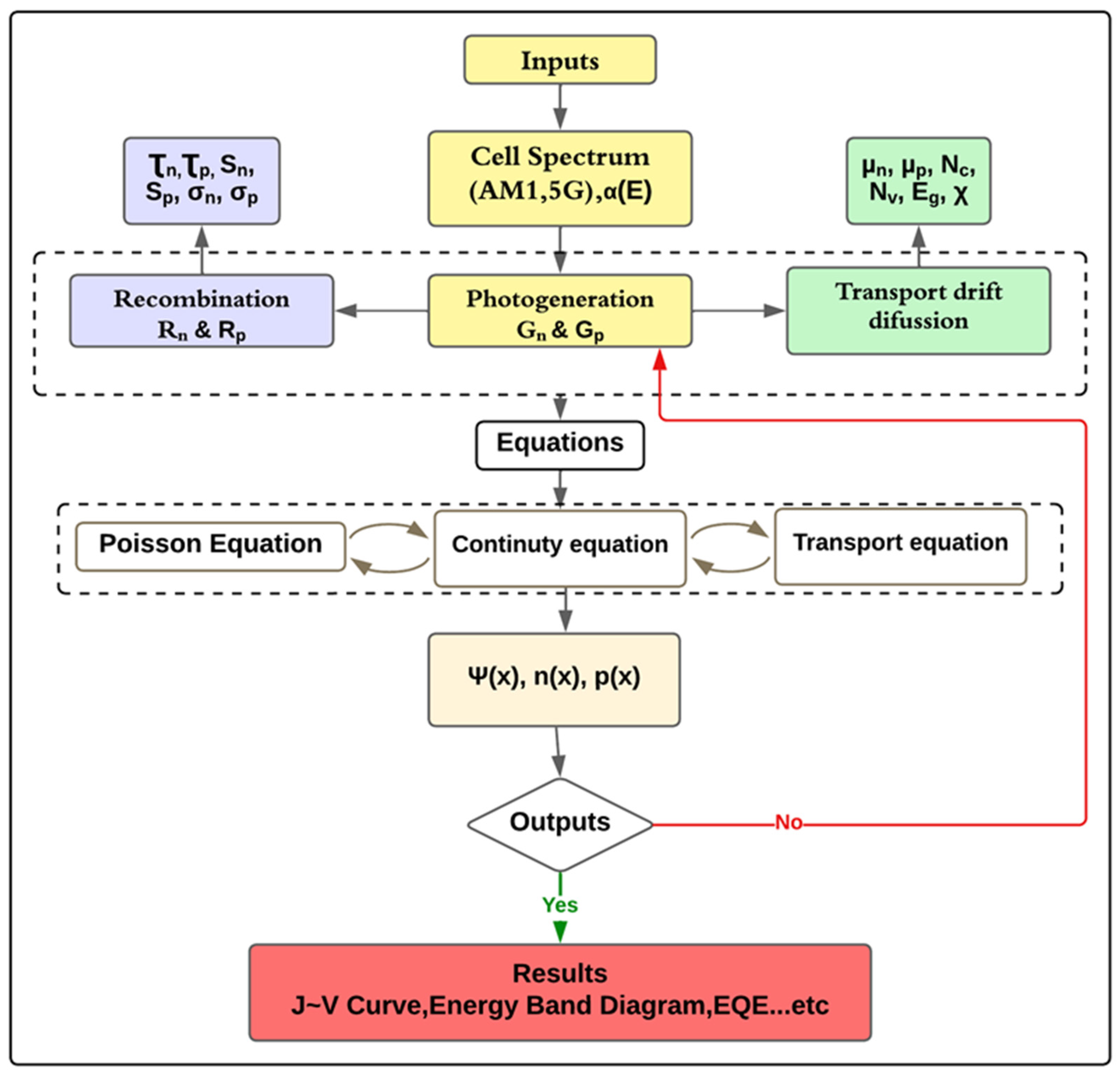
2.1. Simulation of the Proposed Configuration
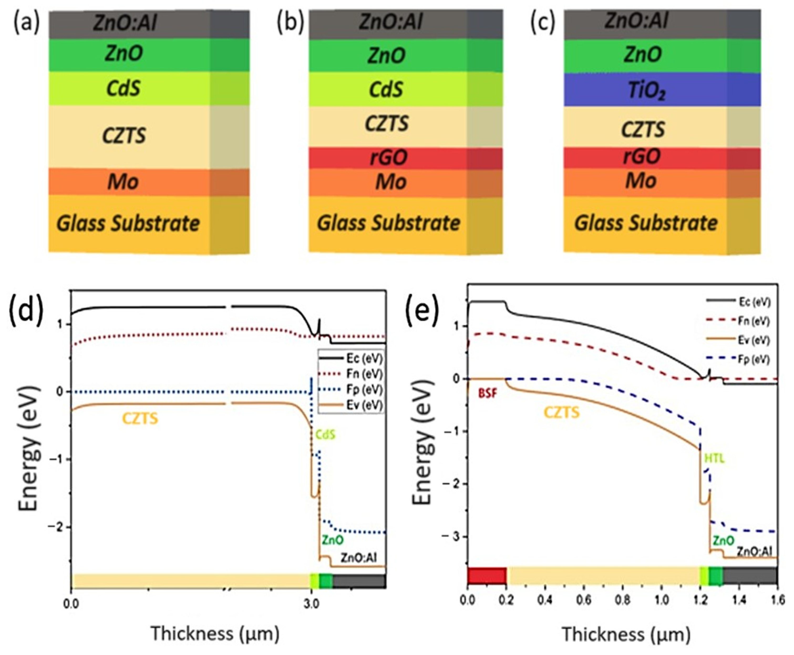
SCAPS is a popular software tool that helps to simulate and analyze how semiconductor devices work. It achieves this by solving key equations from semiconductor physics, like Poisson’s equation, continuity equation, and drift–diffusion equation. Figure 1 displays a flowchart of the SCAPS-1D simulation steps. These equations explain how charge carriers, which are electrons and holes, act when affected by electric fields and temperature. Poisson’s equation can be written as follows:
d 2 ψ ( x ) d x 2 = e ε 0 ε r x n ( x ) + N D N A + ρ p ρ n
where ψ represents the electrostatic potential (V), ρ denotes the charge density (C/m3), NA (m−3) and ND (m−3) refer to the densities of acceptors and donors (m−3), respectively, e stands for the elementary charge (1.6 × 10⁻¹⁹ C), ε0 is the permittivity of free space (F/m), εᵣ(x) signifies the relative permittivity (or dielectric constant), and n(x) indicates the concentration of carriers (m−3).
The continuity equations for electrons and holes are specified as follows [45]:
1 q   J n d x = G R
1 q   J p d x = G R
where Jn and Jp are for electron and hole currents, q is the charge (Coulomb, C), G is the rate of producing electron–hole pairs, and R is the rate of recombining these pairs. The current densities for electrons and holes (A/m2) can be written as follows:
J n = D n d n d x + μ n n d Φ d x
J p = D p d n d x + μ p p d Φ d x
where µn and µp are the mobilities of electrons and holes (cm2/Vs), Dn and Dp are the coefficients for electron and hole diffusion (m2/s), and ϕ refers to the electrostatic potential. SCAPS uses numerical techniques to forecast how semiconductor devices behave, using material properties, shape, and boundary conditions as inputs, and it provides electrical features such as I-V and C-V curves as outputs.

Configurations

  • Conventional CZTS SC without BSF Layer.
This configuration represents a traditional CZTS SC structure without additional layers to reduce recombination losses at the back contact.
2.
CZTS SC with rGO BSF Layer.
A CZTS SC structure is modified in this configuration by incorporating an rGO BSF layer. The rGO layer aims to enhance SC performance by reducing recombination losses at the back contact.
3.
CZTS SC with TiO2 Buffer Layer:
The CZTS SC structure is further modified by replacing the CdS buffer layer with a TiO2 buffer layer. The TiO2 buffer layer aims to improve SC performance by minimizing recombination losses at the buffer–absorber interface.
Figure 2 shows three types of CZTS SC structures: Figure 2a displays a standard structure that does not have a BSF layer, Figure 2b exhibits a structure with an rGO BSF layer, and Figure 2c shows a structure with a titanium dioxide (TiO2) buffer layer. The rGO and TiO2 layers improve SC efficiency by serving as BSF layers between the solar absorber and the back metal contact or buffer–absorber interface. The bandgap of rGO changes based on how it is made and its reduction level. Typically, GO has a larger bandgap than graphene because oxygen-containing groups hinder the lattice structure of graphene. rGO eliminates some of these groups and restores the lattice structure, which lowers the bandgap. GO generally has a bandgap around 2.2 eV [45], while rGO shows a bandgap between 1.00 and 1.69 eV [45,46,47], depending on the reduction process. An rGO bandgap of 1.09 eV is commonly used [48].

2.2. Material Parameters

Numerical simulations, especially with the SCAPS program, have been important for improving our knowledge of chalcogenide-based SCs. SCAPS uses basic semiconductor physics formulas, like continuity equations for electrons and holes and Poisson’s equation. It allows for a significant level of customization in parameters, such as bandgap, electron affinity, mobility, and doping, among others. There are different lighting spectra to choose from, like AM0, AM1.5D, and monochromatic, along with standard test conditions (STCs) such as global air mass (AM 1.5G), 300 K, and 1000 W/m2 of light power. The characteristics of the layers used for the simulated SCs are shown in Table 1.

3. Results

3.1. Part I: Conventional CZTS SC

SCAPS was used to look at how making the absorber layer thinner affects the photoelectrical features of CZTS SCs. The numerical results also showed how adding rGO and TiO2 as BSF or buffer layers influences the performance of the device. The research examined the effects of changing the thickness of the CZTS and BSF layers, along with the role of temperature on the SC’s photovoltaic properties.

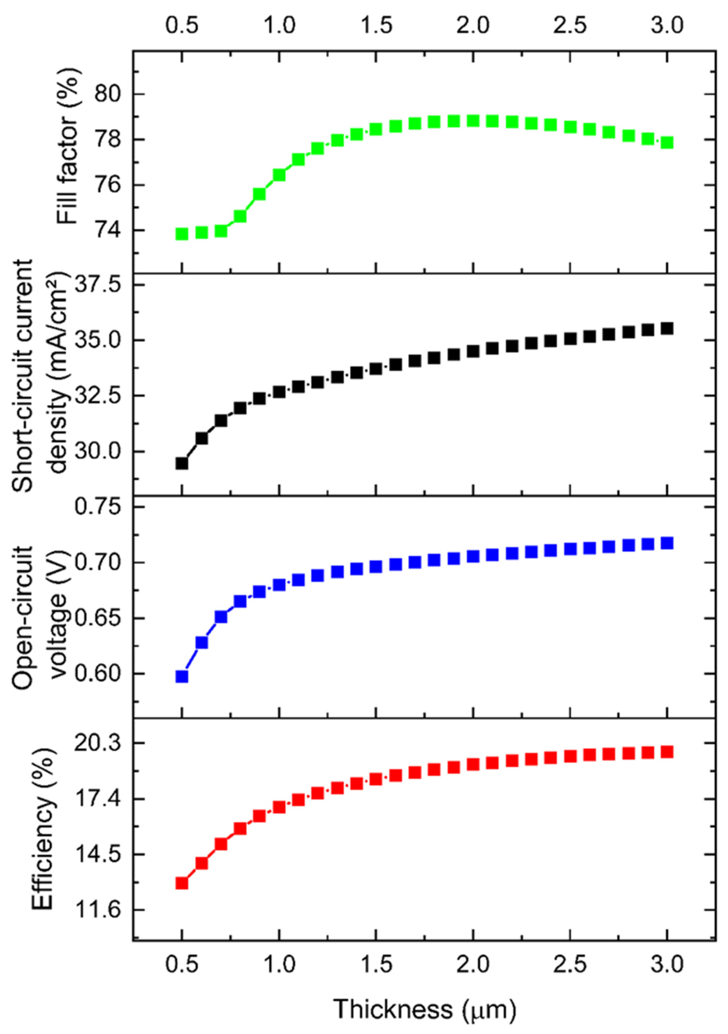
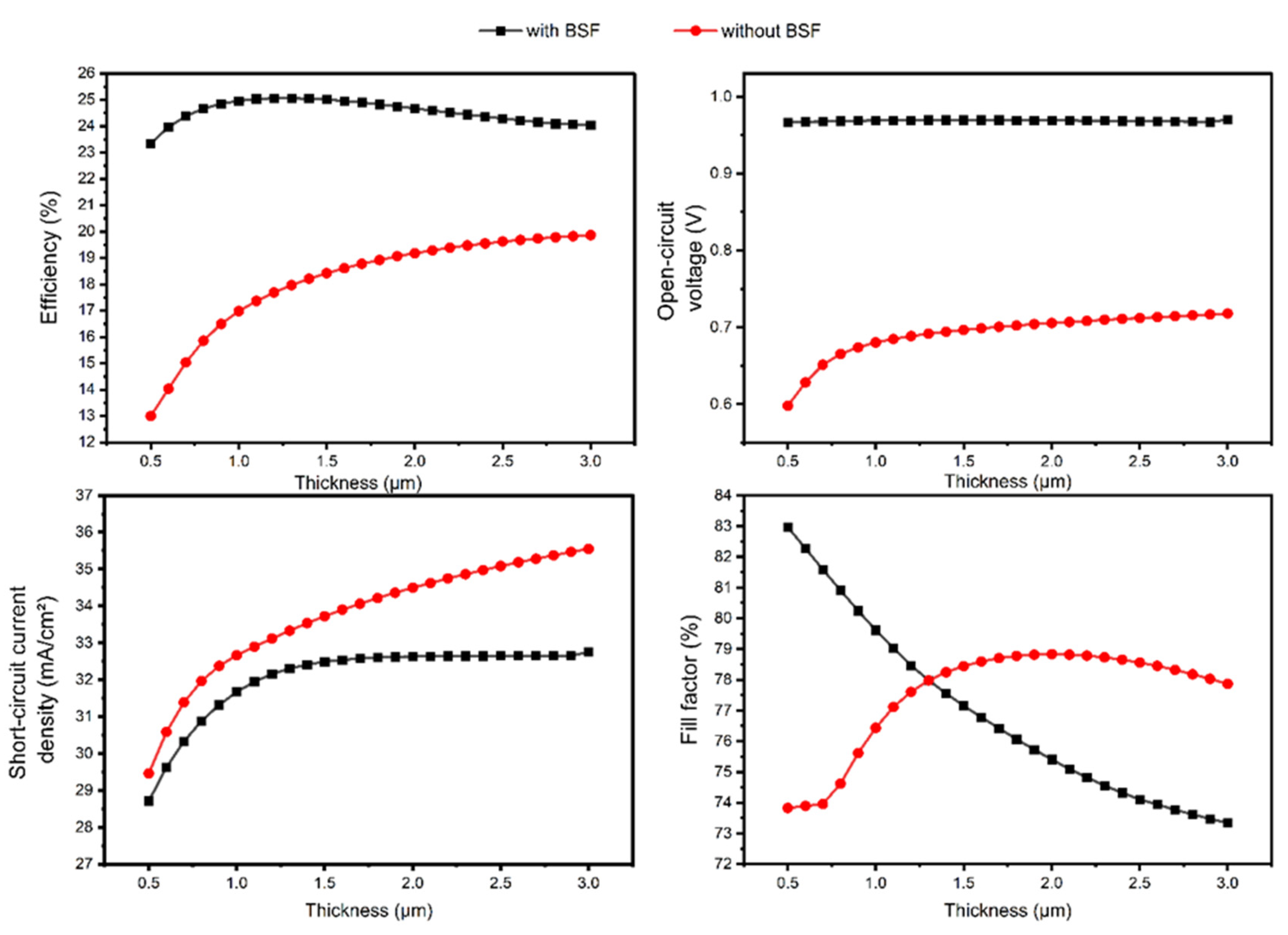
3.1.1. Thickness Optimization of the CZTS Absorber Layer

This part looks at how ZnO/CdS/CZTS SCs perform with different thicknesses of the CZTS absorber layer, based on the details in Table 1. The main aim is to find the best absorber layer thickness for these cells. Figure 3 illustrates the variations in the fill factor (FF), open-circuit voltage (VOC), short-circuit current density (JSC), and efficiency (η) as the p-CZTS absorber layer thickness changes from 0.5 to 3 µm. The FF reaches its highest point around 1.5 µm before slowly declining. JSC progressively increases with thickness, reaching a plateau beyond 2 µm, indicating increased photon absorption and electron-hole pair production, with diminishing returns thereafter. VOC exhibits a quick initial rise and gradual stabilization beyond 2 µm, indicating lower recombination rates at the CZTS–Mo interface in thicker films. Efficiency climbs from 13% to 19.87% as thickness grows from 0.5 µm to 3 µm, with a strong rise up to around 1 µm. More gradually, it stabilizes beyond 2 µm, suggesting no substantial change in efficiency. So. the increase in JSC and VOC improved overall efficiency.
As an illustration, at a CZTS thickness level of 1 µm, the device conversion efficiency increases by 16.98% with the Mo layer [54]. Therefore, an optimal thickness of 1 µm to 2 µm is recommended for the p-CZTS absorber layer to balance all performance parameters effectively.

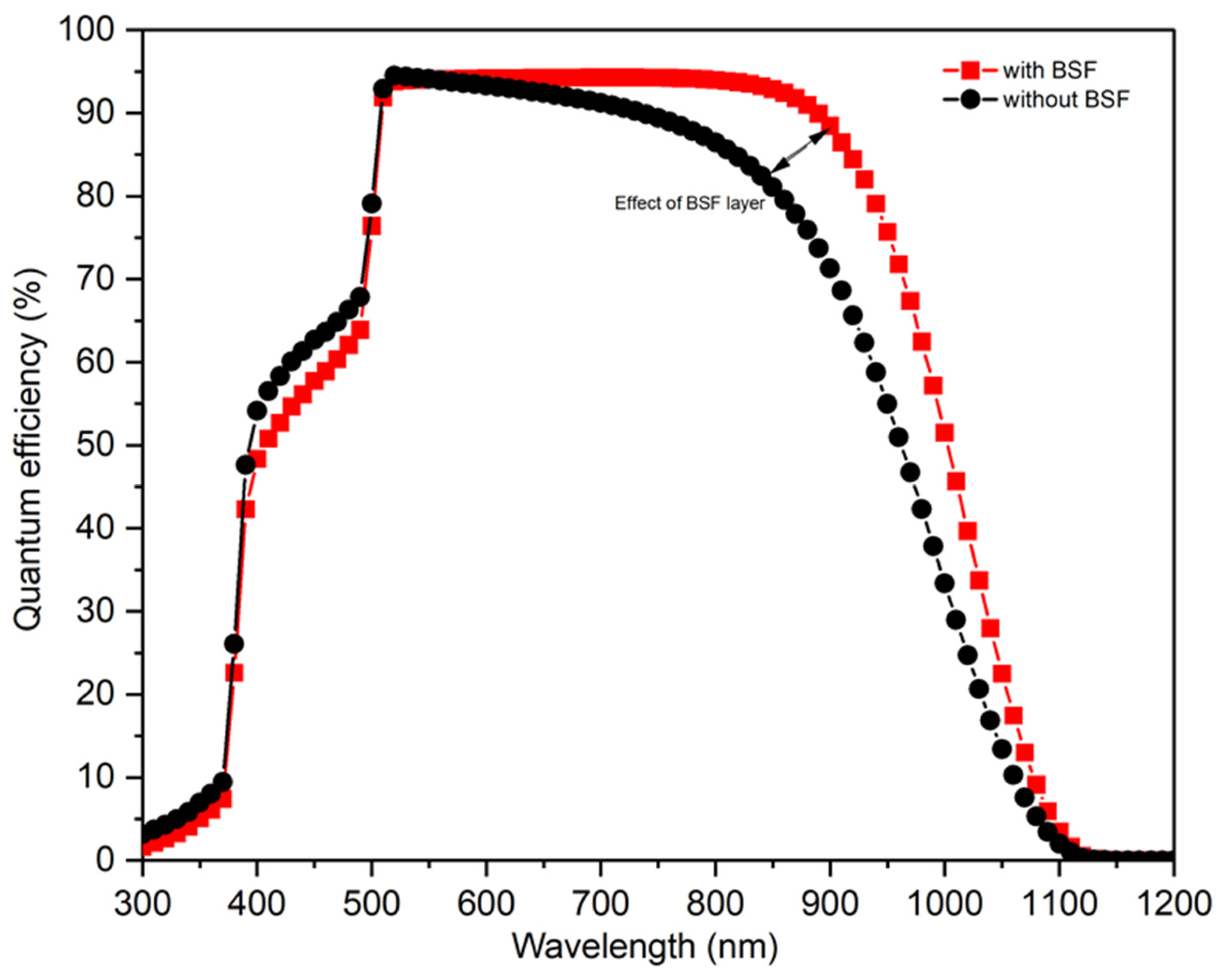
3.1.2. Quantum Efficiency of the CZTS Layer with Various Thicknesses

Figure 4 shows the quantum efficiency (QE) of a material as a function of wavelength, ranging from 300 to 1200 nm, for different absorber layer thicknesses. There are five solid curves and one dashed curve, each corresponding to different thicknesses of the absorber layer: 0.5 µm (black), 1 µm (red), 1.5 µm (green), 2 µm (yellow), 2.5 µm (blue), and 3 µm (purple). All curves show a similar trend, with QE increasing sharply at shorter wavelengths, peaking, and then gradually decreasing at longer wavelengths. Thinner layers, like the 0.5 µm curve, show the lowest QE, while thicker layers, particularly around 2 to 2.5 µm, show the highest and most stable QE across the wavelength range. Beyond 2.5 µm, the improvements in QE are marginal, indicating diminishing returns. Notably, there is no significant change in QE beyond a thickness of 2.5 µm, suggesting that increasing the thickness further does not substantially enhance performance.

3.1.3. Current Flow (J) Related to Voltage (V)

Figure 5 displays the current density (J) as a function of voltage (V). Initially, the current density remains around zero until around 0.60 Volt, suggesting limited current flow. Around 0.60 Volt, a rapid rise in current density indicates the start of considerable current flow when the device approaches its threshold voltage. Beyond this threshold, the current density significantly increases, indicating a significant link between voltage and current density at higher voltages.

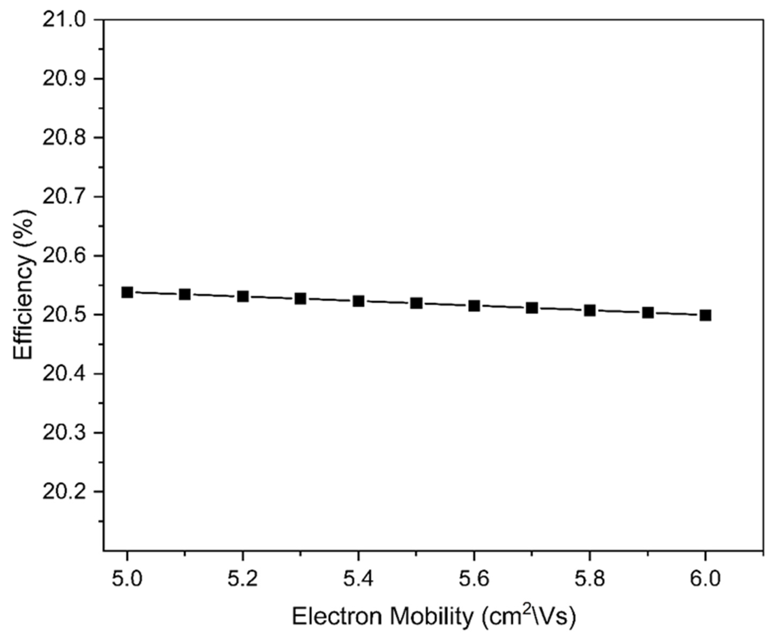
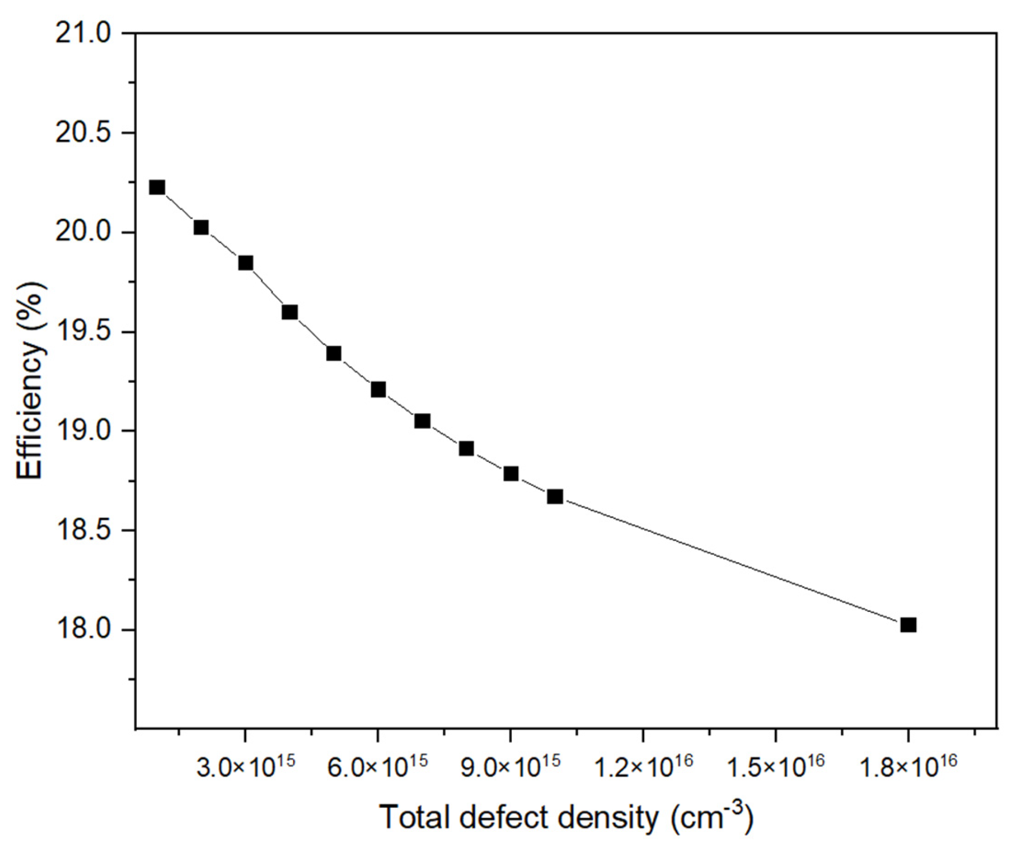
3.1.4. Impact of Electron Mobilities and Total Defect Density of the Absorber Layer

Figure 6 shows the relationship between electron mobility and η of a material, likely in the context of a semiconductor or electronic device. The plot indicates that as the electron mobility increases from 5 cm2/Vs to 6 cm2/Vs, the efficiency of the device or material also increases, although the increase is slight. The efficiency starts around 20.54% and gradually decreases to just above 20.50% as electron mobility improves.
This shows that increased electron mobility improves the device’s efficiency, even if the gain is slight. The pattern suggests that increasing electron mobility can improve performance, but efficiency improvements may plateau beyond specific mobility values.
The overall defect density in the active layer is another important element that can greatly influence how well the device works. The performance of thin-film SCs relies on how good the interfaces are and the presence of defects like point defects, dislocations, stacking faults, and grain boundaries [55]. Defects in the absorber layer that cause a greater frequency of pinholes and recombination result in accelerated film deterioration, decreased stability, and lower device performance overall. The efficiency of the device is impacted by carrier recombination, which is increased by increased defect density.
Figure 7 depicts the link between the overall defect density and efficiency. The graph shows a decreasing trend, demonstrating that as overall defect density grows, efficiency falls. As defect density rises, efficiency decreases from approximately 20% to 18%.

3.2. Part 2: CZTS with BSF Layer (rGO)

Figure 8 shows that introducing a BSF to the SC increases its performance, especially at a thickness of 1.0 µm. At this thickness, the η increased from 16.98% without BSF to around 24.97% in the presence of rGO. Similarly, the Voc is consistently higher with BSF (about 0.97 V) than without it (0.68 V). BSF stabilizes the Jsc at around 32.66 mA/cm2, slightly higher than the 31.67 mA/cm2 compared to CZTS without rGO. The FF decreases significantly with BSF, from 82.96% at 0.5 µm to 73.34% at 3 µm, while remaining stable at roughly 79% in the absence of BSF. As a result, BSF improves current and voltage while decreasing FF as thickness grows.
Figure 9 compares the quantum efficiency spectra of CZTS SCs with and without a BSF layer. QE is significantly improved throughout the wavelength range when the BSF layer is present. At 550 nm, the device reaches a high efficiency of around 94%, whereas the device without the BSF reaches a peak of about 84%. This enhancement is because the BSF layer increases photon absorption and electron–hole pair formation by reflecting unabsorbed photons back into the CZTS absorber layer. This effect is most noticeable in the wavelength range of 500 to 1000 nm, when the device with the BSF retains a significantly higher QE, indicating better production of charge carriers and light harvesting. The QE of both devices decreases as the wavelength of the photons absorbed by the CZTS material increases, which indicates the technology’s inherent limitations. The results highlight the crucial function of the BSF layer in maximizing the visible to near-infrared spectrum response of CZTS SCs, which greatly improves the devices’ overall efficiency and performance.
Figure 10 demonstrates the J-V characteristic curve comparison of CZTS solar cells (SCs) with and without a BSF. The addition of a BSF (red curve) improves open-circuit voltage (Voc) and current density, indicating enhanced charge collection and reduced recombination losses. In contrast, the CZTS cell without a BSF (black curve) exhibits lower Voc and increased recombination losses. This confirms that incorporating a BSF enhances device performance by improving carrier transport and minimizing recombination.
Figure 11 shows how adjusting the thickness of the rGO layer affects the performance parameters of CZTS SCs, including FF, Jsc, Voc, and overall η. The FF slightly declines from 79.41% at 0.2 µm to 78.13% at 1 µm, indicating a minor negative effect as rGO thickness increases. Conversely, Jsc improves from 32.49 mA/cm2 to 32.55 mA/cm2, and Voc rises from 0.97 V to 0.99 V over the same thickness range, suggesting enhanced photon absorption and charge separation. These gains lead to an overall efficiency increase, demonstrating that thicker rGO layers enhance SC performance, despite the slight reduction in FF. Notably, beyond a thickness of 0.5 µm, the performance metrics show minimal change, indicating that further increases in rGO thickness offer diminishing returns on performance enhancements.

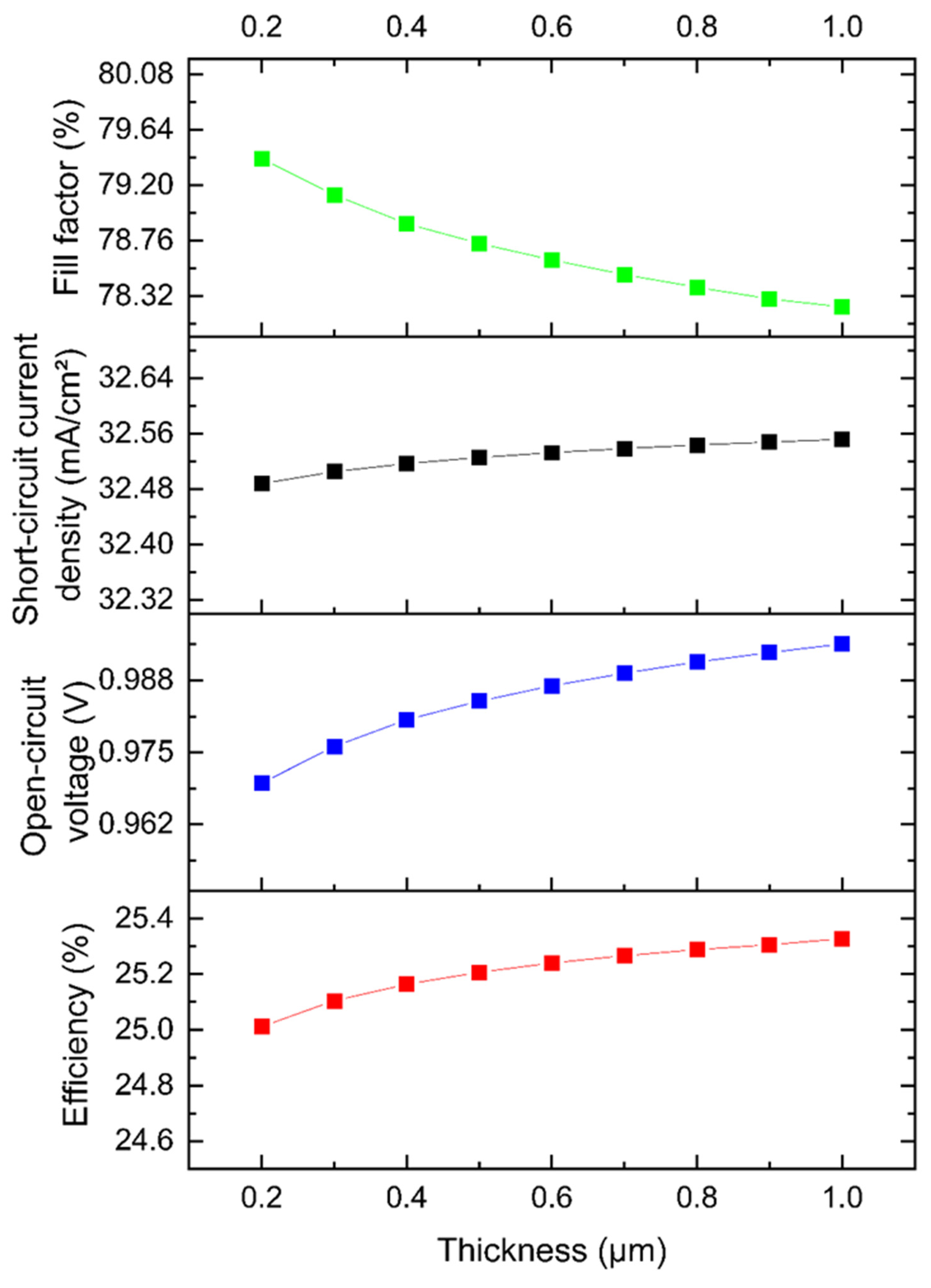
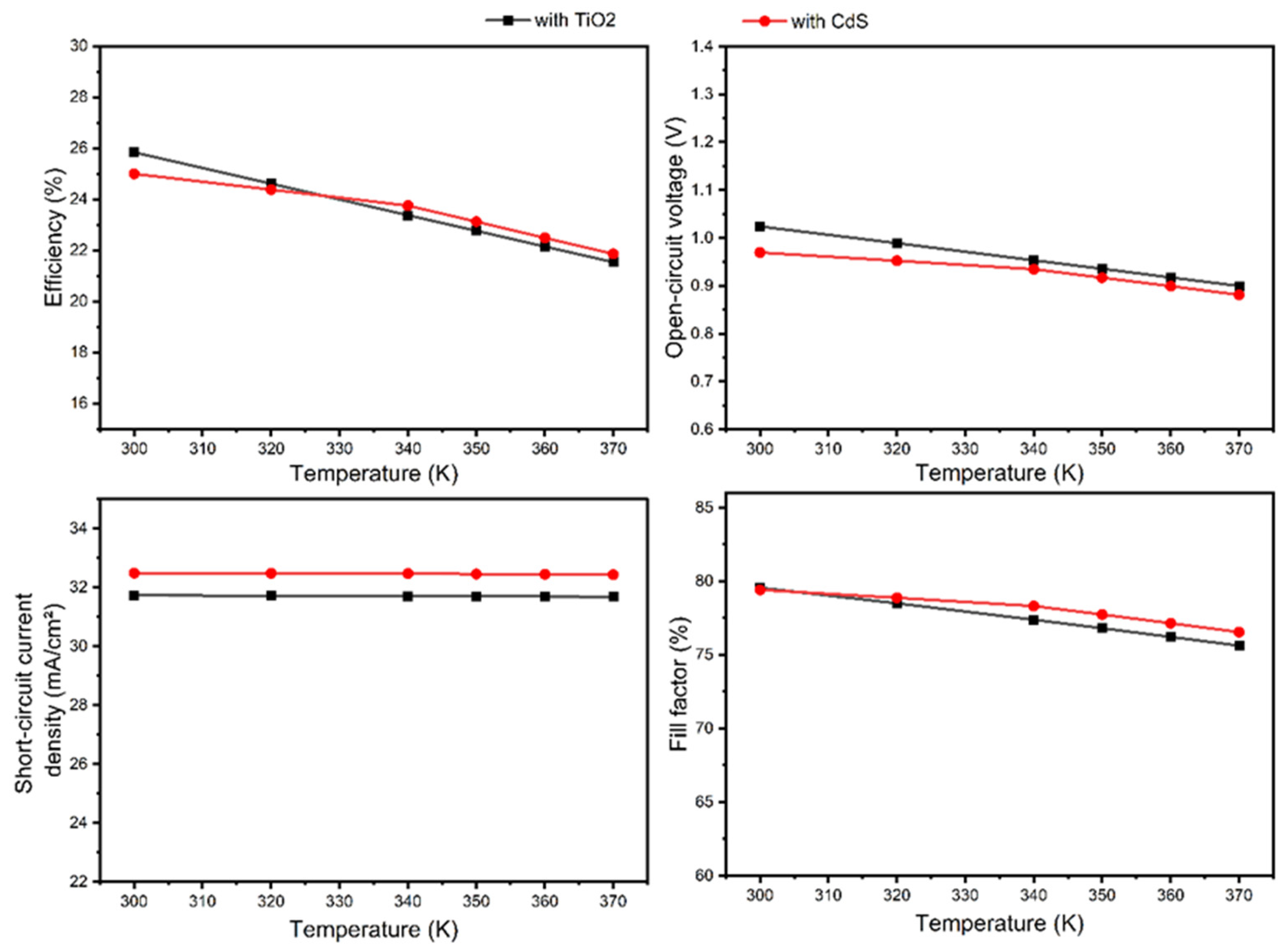
3.3. Part 3: CZTS SC with TiO2 Buffer Layer

Figure 12 shows that for CZTS SCs with CdS and TiO2 buffer layers, η initially increases with thickness, peaking around 26% for TiO2 and 25.50% for CdS, before gradually decreasing. TiO2 consistently provides higher Voc than CdS, with Voc decreasing from about 1.025 V to 1.005 V for TiO2 and from 1.015 V to 1.000 V for CdS as thickness increases. Both buffer layers yield similar Jsc, stabilizing around 33 mA/cm2. However, CdS exhibits a slightly higher FF, decreasing from 82% to 72%, compared to TiO2. TiO2 offers better efficiency, mainly thanks to the increased Voc, while CdS has a marginally higher FF. Additionally, Nisika reported on the TiO2 conductivity connected to oxygen vacancies, which has a significant impact on charge extraction and enhances it in the presence of reduced oxygen levels [56,57]. It is suggested to introduce controlled oxygen vacancies in TiO2 to enhance charge extraction and improve overall device performance. Optimizing the oxygen vacancy concentration could increase Voc and efficiency in CZTS SCs further.
Figure 13 shows that for SCs with a BSF, as the buffer layer thickness increases from 0.05 µm to 0.15 µm, the η decreases from about 26% to 24% for TiO2 and from 25.50% to 23.50% for CdS. The Voc was approximately 1.02 V for TiO2 and 1.02 V for CdS. The Jsc decreases from around 31.80 mA/cm2 to 29.80 mA/cm2 for TiO2 and from 31.60 mA/cm2 to 29.50 mA/cm2 for CdS. The FF shows a slight decrease from 79.56% to 79.30% for TiO2 and 79.40% to 79.10% for CdS. From an experimental perspective, few studies have been published, but recently, highly promising findings have been generated [58,59]. This study pioneers a Cd-free superstrate configuration, achieving a record efficiency of 9.7% for ultrathin (Cu,Ag)2ZnSn(S,Se)4 SCs with a TiO2 buffer layer to enhance performance.
Figure 14 shows the temperature-dependent performance study of CZTS SCs with TiO2 and CdS buffer layers. As the temperature rises, both buffer layers’ efficiency and Voc drop. TiO2 has an initial efficiency of 26% at 300 K and decreases to 21.50% at 370 K. CdS has a lower efficiency of roughly 25% and decreases to 21.50% at the same temperature. This graph highlights TiO2’s higher efficiency and a slower rate of decrease compared to CdS. TiO2 maintains higher Voc values over the temperature range, reducing from 1.01 V to 0.89 V, whereas CdS decreases from 0.97 V to 0.88 V. Although both materials have reasonably steady Jsc, CdS has a higher Jsc (32.48 mA/cm2) than TiO2 (31.73 mA/cm2). However, the fill factor (FF) decreases with temperature. CdS and TiO2 initially have a FF (79% at 300 K), but both fall to 76.50% and 75.62%, respectively, at 370 K. TiO2 outperforms CdS in terms of efficiency, Voc, thermal stability, and resilience. Despite slightly higher FF, CdS cannot match TiO2’s performance throughout temperature ranges.
Figure 15 compares the current density–voltage (J-V) characteristic among three CZTS-based SC configurations: standard CZTS and CZTS with a BSF, and CZTS with a TiO2 layer. The figure shows that adding BSF and TiO2 improves the cells’ performance, as both configurations exhibit higher Voc than standard CZTS. The improved Voc suggests better overall performance for the modified configurations, especially for CZTS with TiO2, which shows the highest Voc.
Table 2 shows that the effectiveness of CZTS SCs is significantly improved by incorporating TiO2 and a BSF. The Jsc slightly decreases from 33.72 mA/cm2 (standard CZTS) to 32.49 mA/cm2 (CZTS with BSF) and 32.65 mA/cm2 (CZTS with TiO2). However, the Voc increases significantly, from 0.70 V (standard CZTS) to 0.97 V (with BSF) and 1.02 V (with TiO2).
Although the FF remains relatively stable, with slight decreases from 78.44% (standard CZTS) to 77.15% (BSF) and 77.06% (TiO2), the overall η improves considerably. The efficiency rises from 18.42% (standard CZTS) to 25.01% (BSF) and 25.68% (TiO2), indicating that the TiO2 configuration provides the best performance enhancement.

4. Conclusions

The theoretical modeling of CZTS SCs with an rGO BSF and TiO2 as a buffer layer has demonstrated promising advancements in SC efficiency. By precisely tuning the composition and thickness of these layers, this study achieved a predicted efficiency of 25.68%, significantly outperforming conventional SCs. The rGO BSF layer effectively reduced back surface recombination and created a quasi-ohmic contact, contributing to enhanced performance. Moreover, replacing the conventional CdS buffer layer with non-toxic TiO2 further improved the cell’s overall efficiency to 25.68% while offering a more environmentally sustainable solution.
The success of this modeled structure underscores the potential of advanced materials like rGO and TiO2 in pushing the limits of thin-film photovoltaic technologies. This research highlights the pivotal role of BSF layers and opens new avenues for developing high-efficiency, eco-friendly SCs, contributing to the future of renewable energy solutions.

Author Contributions

Conceptualization, D.F.; software and theoretical calculations, D.F.; visualization, D.F., A.K. and R.A.; validation, D.F. and R.A.; formal analysis, D.F.; investigation, D.F., R.A. and N.A.; resources, R.A. and P.S.; data curation, G.T., V.T., S.B. and E.I.; writing—original draft preparation, D.F.; writing—review and editing, D.F., A.K., R.A., N.A., V.T., G.T., S.B., P.S. and E.I.; visualization, D.F., A.K. and R.A.; supervision, R.A., A.K., N.A. and P.S.; project administration, R.A.; funding acquisition, R.A., N.A. and P.S. All authors have read and agreed to the published version of the manuscript.

Funding

This research received no external funding.

Data Availability Statement

The data presented in this study are available on request from the corresponding author.

Acknowledgments

The authors thank Marc Burgelman and his team at the Department of Electronics and Information Systems (ELIS), University of Gent, Belgium, for providing the SCAPS software package, version 3.3.07. The authors would like to express their gratitude to the Ministry of Foreign Affairs and International Cooperation (MAECI) for their invaluable support in funding and facilitating this project. In addition, the sixth and the last authors acknowledge the support of the Italian Ministry of Universities and Research (MUR), in the framework of the project DICAM-EXC (Departments of Excellence 2023–2027, grant L232/2016).

Conflicts of Interest

The authors declare no conflicts of interest.

Abbreviations

The following abbreviations are used in this manuscript:
CZTSCopper zinc tin sulfide (commonly known as CZTS)
CdSCadmium sulfide
TiO2Titanium dioxide
ZnOZinc oxide
AlAluminuim
MoMolybdenum
ALDAtomic layer deposition
CBDChemical bath deposition
SCSolar cell
BSFBack surface field
SCAPSSolar Cell Capacitance Simulator
rGOReduced graphene oxide
CIGS Copper, gallium, indium and selenium
VOCOpen Circuit current
JscShort-circuit current density
FF Fill factor
ηEfficiency
QEQuantum efficiency
εᵣ(x) Dielectric constant
ε0Permittivity of free space
n(x) Concentration of carriers
JnCurrent density of electron
JpCurrent density of hole
eElementary charge
ψElectrostatic potential
ρCharge density
NADensity of acceptors
NDDensity of acceptors and donors
GRate of producing electron–hole pairs
µnMobility of electrons
µpMobility of holes
ϕElectrostatic potential
DnCoefficient of electron diffusion
DpCoefficient of hole diffusion
JCurrent density
VVoltage

References

  1. Yang, X.; Qin, X.; Yan, W.; Zhang, C.; Zhang, D.; Guo, B. Electronic Structure and Optical Properties of Cu2ZnSnS4 under Stress Effect. Crystals 2022, 12, 1454. [Google Scholar] [CrossRef]
  2. Soonmin, H.; Hardani Nandi, P.; Mwankemwa, B.S.; Malevu, T.D.; Malik, M.I. Overview on Different Types of Solar Cells: An Update. Appl. Sci. 2023, 13, 2051. [Google Scholar] [CrossRef]
  3. Vilanova, A.; Dias, P.; Lopes, T.; Mendes, A. The route for commercial photoelectrochemical water splitting: A review of large-area devices and key upscaling challenges. Chem. Soc. Rev. 2024, 53, 2388–2434. [Google Scholar] [CrossRef] [PubMed]
  4. Kumar, Z.A.; Ahmad, T.; Ansari, M.Z. Chapter Nine—Copper zinc tin sulfide thin-film solar cells: An overview. In Photovoltaics Beyond Silicon; Solar Cell Engineering; Elsevier: Amsterdam, The Netherlands, 2024; pp. 303–322. [Google Scholar] [CrossRef]
  5. Tseberlidis, G.; Trifiletti, V.; Le Donne, A.; Frioni, L.; Acciarri, M.; Binetti, S. Kesterite solar-cells by drop-casting of inorganic sol–gel inks. Sol. Energy 2020, 208, 532–538. [Google Scholar] [CrossRef]
  6. Trifiletti, V.; Mostoni, S.; Butrichi, F.; Acciarri, M.; Binetti, S.; Scotti, R. Study of Precursor-Inks Designed for High-Quality Cu2ZnSnS4 Films for Low-Cost PV Application. ChemistrySelect 2019, 4, 4905–4912. [Google Scholar] [CrossRef]
  7. Panzeri, G.; Dell’Oro, R.; Trifiletti, V.; Parravicini, J.; Acciarri, M.; Binetti, S.; Magagnin, L. Copper electrodeposition onto zinc for the synthesis of kesterite Cu2ZnSnS4 from a Mo/Zn/Cu/Sn precursor stack. Electrochem. Commun. 2019, 109, 106580. [Google Scholar] [CrossRef]
  8. Islam, M.S.; Doroody, C.; Kiong, T.S.; Rahman, K.S.; Zuhdi, A.W.M.; Yap, B.K.; Alam, M.N.-E.; Amin, N. MoS2 thin film hetero-interface as effective back surface field in CZTS-based solar cells. Mater. Sci. Semicond. Process. 2024, 182, 108721. [Google Scholar] [CrossRef]
  9. Banerjee, A.; Sarkar, A.; Shukla, S.; Saxena, S.; Banerjee, A.; Guchhait, A.; Lawaniya, R.; Kumar, A.; Dalapati, G.K. Chapter 9—Sulfide and selenide-based flexible and semitransparent solar cells for building integrated photovoltaics. In Sulfide and Selenide Based Materials for Emerging Applications; Dalapati, G., Shun Wong, T., Kundu, S., Chakraborty, A., Zhuk, S., Eds.; Elsevier: Amsterdam, The Netherlands, 2022; pp. 179–194. [Google Scholar] [CrossRef]
  10. Su’ait, M.S.; Sahudin, M.A.; Ludin, N.A.; Ahmad, A.; Rahman, M.Y.A.; Ahmoum, H.; Ataollahi, N.; Scardi, P. Potential of transition metal sulfides, Cu2ZnSnS4 as inorganic absorbing layers in dye-sensitized solar cells. J. Clean. Prod. 2023, 394, 136327. [Google Scholar] [CrossRef]
  11. Ataollahi, N.; Bazerla, F.; Malerba, C.; Chiappini, A.; Ferrari, M.; Di Maggio, R.; Scardi, P. Synthesis and post-annealing of Cu2ZnSnS4 absorber layers based on Oleylamine/1-dodecanethiol. Materials 2019, 12, 3320. [Google Scholar] [CrossRef]
  12. Yussuf, S.T.; Oranzie, M.; Cox, M.; Xia, R.; Admassie, S.; January, J.L.; Peng, X.; Iwuoha, E.I. Microwave-synthesized aluminum, gallium and indium-substituted stannite nanocrystal absorbers for solar cell applications. Mater. Today Sustain. 2024, 26, 100771. [Google Scholar] [CrossRef]
  13. Huang, C.H.; Chuang, W.J. Dependence of performance parameters of CdTe solar cells on semiconductor properties studied by using SCAPS-1D. Vacuum 2015, 118, 32–37. [Google Scholar] [CrossRef]
  14. Romeo, A.; Artegiani, E. CdTe-Based Thin Film Solar Cells: Past, Present and Future. Energies 2021, 14, 1684. [Google Scholar] [CrossRef]
  15. Buonomenna, M.G. Inorganic Thin-Film Solar Cells: Challenges at the Terawatt-Scale. Symmetry 2023, 15, 1718. [Google Scholar] [CrossRef]
  16. Ashagre, S.; Ogundele, A.K.; Ike, J.N.; Gebremichael, B.; Bekele, M.; Sharma, G.D.; Mola, G.T. Synergistic contribution of potassium sulfide doped with silver nanoparticles on the performance of thin film organic solar cells. J. Phys. Chem. Solids 2023, 177, 111290. [Google Scholar] [CrossRef]
  17. Keerthi Priya, T.; Deb, P.; Choudhury, A. Simulation of High Efficiency Hybrid FTO/TiO2/CH3NH3SnI3/RGO-Based Solar Cell Using SCAPS-1D. Optik 2024, 316, 172051. [Google Scholar] [CrossRef]
  18. Zhang, J.; Liu, B.; Liu, Z.; Wu, J.; Arnold, S.; Shi, H.; Osterrieder, T.; Hauch, J.A.; Wu, Z.; Luo, J.; et al. Optimizing Perovskite Thin-Film Parameter Spaces with Machine Learning-Guided Robotic Platform for High-Performance Perovskite Solar Cells. Adv. Energy Mater. 2023, 13, 2302594. [Google Scholar] [CrossRef]
  19. Ali, S.; Ahmad, K.; Khan, R.A.; Kumar, P. Simulation-Based Studies on FAGeI3-Based Lead (Pb2+)-Free Perovskite Solar Cells. Crystals 2025, 15, 135. [Google Scholar] [CrossRef]
  20. Alsalme, A.; Altowairqi, M.F.; Alhamed, A.A.; Khan, R.A. Optimization of Photovoltaic Performance of Pb-Free Perovskite Solar Cells via Numerical Simulation. Molecules 2023, 28, 224. [Google Scholar] [CrossRef]
  21. Yerezhep, D.; Omarova, Z.; Aldiyarov, A.; Shinbayeva, A.; Tokmoldin, N. IR Spectroscopic Degradation Study of Thin Organometal Halide Perovskite Films. Molecules 2023, 28, 1288. [Google Scholar] [CrossRef]
  22. Alsalme, A.; Alsaeedi, H. Twenty-Two Percent Efficient Pb-Free All-Perovskite Tandem Solar Cells Using SCAPS-1D. Nanomaterials 2023, 13, 96. [Google Scholar] [CrossRef]
  23. Siddique, A.; Islam, N.; Karmaker, H.; Iqbal, A.A.; Khan, A.A.M.; Islam, A.; Das, B.K. Numerical modelling and performance investigation of inorganic Copper-Tin-Sulfide (CTS) based perovskite solar cell with SCAPS-1D. Results Opt. 2024, 16, 100713. [Google Scholar] [CrossRef]
  24. Chee, A.K.W. On current technology for light absorber materials used in highly efficient industrial solar cells. Renew. Sustain. Energy Rev. 2023, 173, 113027. [Google Scholar] [CrossRef]
  25. Ahmoum, H.; Su’ait, M.S.; Ataollahi, N.; Mustaffa, M.U.S.; Boughrara, M.; Chelvanathan, P.; Sopian, K.; Li, G.; Kerouad, M.; Scardi, P.; et al. Suppressing the secondary phases via N2 preheating of Cu2ZnSnS4 thin films with the addition of oleylamine and/or 1-Dodecanethiol solvents. Inorg. Chem. Commun. 2021, 134, 109031. [Google Scholar]
  26. Shah, U.A.; Wang, A.; Irfan Ullah, M.; Ishaq, M.; Alam Shah, I.; Zeng, Y.; Abbasi, M.S.; Umair, M.A.; Farooq, U.; Liang, G.; et al. A Deep Dive into Cu2 ZnSnS4 (CZTS) Solar Cells: A Review of Exploring Roadblocks, Breakthroughs, and Shaping the Future. Small 2024, 20, 2310584. [Google Scholar] [CrossRef]
  27. Le Donne, A.; Trifiletti, V.; Binetti, S. New Earth-Abundant Thin Film Solar Cells Based on Chalcogenides. Front. Chem. 2019, 7, 297. [Google Scholar] [CrossRef]
  28. Dalapati, G.K.; Zhuk, S.; Masudy-Panah, S.; Kushwaha, A.; Seng, H.L.; Chellappan, V.; Suresh, V.; Su, Z.; Batabyal, S.K.; Guchhait, A.; et al. Impact of molybdenum out diffusion and interface quality on the performance of sputter grown CZTS based solar cells. Sci. Rep. 2017, 7, 1350. [Google Scholar] [CrossRef]
  29. Tseberlidis, G.; Trifiletti, V.; Vitiello, E.; Vitiello, E.; Husien, A.H.; Husien, A.H.; Frioni, L.; Da Lisca, M.; Alvarez, J.; Acciarri, M.; et al. Band-Gap Tuning Induced by Germanium Introduction in Solution-Processed Kesterite Thin Films. ACS Omega 2022, 7, 23445–23456. [Google Scholar] [CrossRef]
  30. Lin, J.; Wu, X.; Xu, J.; Yang, Y. Inhibiting the formation of MoS2 between Cu2ZnSnS4 thin film and Mo(211) foil substrate by inserting a Mo(110) intermediate layer. Opt. Mater. 2022, 124, 111996. [Google Scholar] [CrossRef]
  31. Lin, J.; Xu, J.; Yang, Y. Numerical analysis of the effect of MoS2 interface layers on copper-zinc-tin-sulfur thin film solar cells. Optik 2020, 201, 163496. [Google Scholar] [CrossRef]
  32. Srivastava, M.; Banerjee, S.; Bairagi, S.; Singh, P.; Kumar, B.; Singh, P.; Kale, R.D.; Mulvihill, D.M.; Ali, S.W. Recent progress in molybdenum disulfide (MoS2) based flexible nanogenerators: An inclusive review. Chem. Eng. J. 2024, 480, 147963. [Google Scholar] [CrossRef]
  33. Haque, A.; Mamun, M.A.A.; Taufique, M.F.N.; Karnati, P.; Ghosh, K. Temperature Dependent Electrical Transport Properties of High Carrier Mobility Reduced Graphene Oxide Thin Film Devices. IEEE Trans. Semicond. Manuf. 2018, 31, 535–544. [Google Scholar] [CrossRef]
  34. Safian MT uddeen Umar, K.; Mohamad Ibrahim, M.N. Synthesis and scalability of graphene and its derivatives: A journey towards sustainable and commercial material. J. Clean. Prod. 2021, 318, 128603. [Google Scholar] [CrossRef]
  35. Zhao, D.; Wang, P.; Zhao, F.J. Dietary cadmium exposure, risks to human health and mitigation strategies. Crit. Rev. Environ. Sci. Technol. 2022, 53, 939–963. [Google Scholar] [CrossRef]
  36. Tseberlidis, G.; Gobbo, C.; Trifiletti, V.; Di Palma, V.; Binetti, S. Cd-free kesterite solar cells: State-of-the-art and perspectives. Sustain. Mater. Technol. 2024, 41, e01003. [Google Scholar] [CrossRef]
  37. Tseberlidis, G.; Di Palma, V.; Trifiletti, V.; Frioni, L.; Valentini, M.; Malerba, C.; Mittiga, A.; Acciarri, M.; Binetti, S.O. Titania as Buffer Layer for Cd-Free Kesterite Solar Cells. ACS Mater. Lett. 2023, 5, 219–224. [Google Scholar] [CrossRef]
  38. Gobbo, C.; Di Palma, V.; Trifiletti, V.; Malerba, C.; Valentini, M.; Matacena, I.; Daliento, S.; Binetti, S.; Acciarri, M.; Tseberlidis, G. Effect of the ZnSnO/AZO Interface on the Charge Extraction in Cd-Free Kesterite Solar Cells. Energies 2023, 16, 4137. [Google Scholar] [CrossRef]
  39. Razzaq, Z.; Khalid, A.; Ahmad, P.; Farooq, M.; Khandaker, M.U.; Sulieman, A.; Rehman, I.U.; Shakeel, S.; Khan, A. Photocatalytic and Antibacterial Potency of Titanium Dioxide Nanoparticles: A Cost-Effective and Environmentally Friendly Media for Treatment of Air and Wastewater. Catalysts 2021, 11, 709. [Google Scholar] [CrossRef]
  40. Ge, S.; Sang, D.; Zou, L.; Yao, Y.; Zhou, C.; Fu, H.; Xi, H.; Fan, J.; Meng, L.; Wang, C. A Review on the Progress of Optoelectronic Devices Based on TiO2 Thin Films and Nanomaterials. Nanomaterials 2023, 13, 1141. [Google Scholar] [CrossRef]
  41. Cheng, X.; Gotoh, K.; Mochizuki, T.; Usami, N. Controllable Optical and Electrical Properties of Nb-Doped TiO2 Films by RF Sputtering. In Proceedings of the 2018 IEEE 7th World Conference on Photovoltaic Energy Conversion (WCPEC), Waikoloa, HI, USA, 10–15 June 2018; pp. 1986–1990. [Google Scholar] [CrossRef]
  42. Khan, H.; Shah, M.U.H. Modification strategies of TiO2 based photocatalysts for enhanced visible light activity and energy storage ability: A review. J. Environ. Chem. Eng. 2023, 11, 111532. [Google Scholar] [CrossRef]
  43. Houshmand, M.; Esmaili, H.; Zandi, M.H.; Gorji, N.E. Degradation and device physics modeling of TiO2/CZTS ultrathin film photovoltaics. Mater. Lett. 2015, 157, 123–126. [Google Scholar]
  44. Chang, H.; Sun, Z.; Saito, M.; Yuan, Q.; Zhang, H.; Li, J.; Wang, Z.; Fujita, T.; Ding, F.; Zheng, Z.; et al. Regulating Infrared Photoresponses in Reduced Graphene Oxide Phototransistors by Defect and Atomic Structure Control. ACS Nano 2013, 7, 6310–6320. [Google Scholar] [CrossRef] [PubMed]
  45. Abid Sehrawat, P.; Islam, S.S.; Mishra, P.; Ahmad, S. Reduced graphene oxide (rGO) based wideband optical sensor and the role of Temperature, Defect States and Quantum Efficiency. Sci. Rep. 2018, 8, 3537. [Google Scholar] [CrossRef]
  46. Wang, Y.; Chen, Y.; Lacey, S.D.; Xu, L.; Xie, H.; Li, T.; Danner, V.A.; Hu, L. Reduced graphene oxide film with record-high conductivity and mobility. Mater. Today 2018, 21, 186–192. [Google Scholar] [CrossRef]
  47. Mattson, E.C.; Johns, J.E.; Pande, K.; Bosch, R.A.; Cui, S.; Gajdardziska-Josifovska, M.; Weinert, M.; Chen, J.H.; Hersam, M.C.; Hirschmugl, C.J. Vibrational Excitations and Low-Energy Electronic Structure of Epoxide-Decorated Graphene. J. Phys. Chem. Lett. 2014, 5, 212–219. [Google Scholar] [CrossRef]
  48. Jeong, W.L.; Park, S.H.; Jho, Y.D.; Joo, S.K.; Lee, D.S. The Role of the Graphene Oxide (GO) and Reduced Graphene Oxide (RGO) Intermediate Layer in CZTSSe Thin-Film Solar Cells. Materials 2022, 15, 3419. [Google Scholar] [CrossRef]
  49. Shafi, M.A.; Bouich, A.; Fradi, K.; Guaita, J.M.; Khan, L.; Mari, B. Effect of deposition cycles on the properties of ZnO thin films deposited by spin coating method for CZTS-based solar cells. Optik 2022, 258, 168854. [Google Scholar] [CrossRef]
  50. Moghadam Ziabari, S.A.; Abdolahzadeh Ziabari, A.; Mousavi, S.J. Efficiency enhancement of thin-film solar cell by implementation of double-absorber and BSF layers: The effect of thickness and carrier concentration. J. Comput. Electron. 2022, 21, 675–683. [Google Scholar] [CrossRef]
  51. Nowsherwan, G.A.; Hussain, S.S.; Khan, M.; Haider, S.; Akbar, I.; Nowsherwan, N.; Ikram, S.; Ishtiaq, S.; Riaz, S.; Naseem, S. Role of graphene-oxide and reduced-graphene-oxide on the performance of lead-free double perovskite solar cell. Z. Für Naturforschung A 2022, 77, 1083–1098. [Google Scholar] [CrossRef]
  52. Zaidi, B.; Kerboub, A.; Bouarroudj, T.; Shekhar, C.; Mahmood, T.; Saeed, M. Enhancement of Performance of TiO2/Cu2O Solar Cells. J. Optoelectron. Adv. Mater. 2023, 25, 549–553. [Google Scholar]
  53. Liu, X.; Hu, Y. Investigation of TiO2 as the buffer layer in wide bandgap chalcopyrite solar cells using SCAPS. J. Mater. Sci. Mater. Electron. 2022, 33, 6253–6261. [Google Scholar] [CrossRef]
  54. Kumari, N.; Ingole, S. Enhancement of CZTS photovoltaic device performance with silicon at back-contact: A study using SCAPS-1D. Solar Energy 2022, 236, 301–307. [Google Scholar] [CrossRef]
  55. Gupta, G.K.; Dixit, A. Effect of precursor and composition on the physical properties of the low-cost solution processed Cu2ZnSnS4 thin film for solar photovoltaic application. J. Renew. Sustain. Energy 2017, 9, 013502. [Google Scholar] [CrossRef]
  56. Nisika Ghosh, A.; Kaur, K.; Bobba, R.S.; Qiao, Q.; Kumar, M. Engineering Cu2ZnSnS4 grain boundaries for enhanced photovoltage generation at the Cu2ZnSnS4/TiO2 heterojunction: A nanoscale investigation using Kelvin probe force microscopy. J. Appl. Phys. 2021, 130, 195301. [Google Scholar] [CrossRef]
  57. Nisika Kaur, K.; Arora, K.; Bobba, R.S.; Qiao, Q.; Kumar, M. Energy level alignment and nanoscale investigation of a TiO2/Cu-Zn-Sn-S interface for alternative electron transport layer in earth abundant Cu-Zn-Sn-S solar cells. J. Appl. Phys. 2019, 126, 193104. [Google Scholar] [CrossRef]
  58. Wang, Z.; Wang, Y.; Taghipour, N.; Peng, L.; Konstantatos, G. Ag-Refined Kesterite in Superstrate Solar Cell Configuration with 9.7% Power Conversion Efficiency. Adv. Funct. Mater. 2022, 32, 2205948. [Google Scholar] [CrossRef]
  59. Bencherif, H.; Dehimi, L.; Mahsar, N.; Kouriche, E.; Pezzimenti, F. Modeling and optimization of CZTS kesterite solar cells using TiO2 as efficient electron transport layer. Mater. Sci. Eng. B 2022, 276, 115574. [Google Scholar] [CrossRef]
Figure 1. Flowchart of the SCAPS-1D simulation process, highlighting key input parameters, semiconductor equations, and output evaluation.
Chemengineering 09 00038 g001
Figure 2. Comparison of (a) the designs for a conventional CZTS SC without a BSF layer, (b) a proposed cell with an rGO BSF layer, (c) a proposed cell with a TiO2 buffer layer, (d) band gap of conventional SCs, and (e) band gap of proposed cell with BSF layer.
Chemengineering 09 00038 g002
Figure 3. Photovoltaic performance metrics of CZTS CSs as a function of absorber layer thickness, including FF, VOC, JSC, and η.
Chemengineering 09 00038 g003
Figure 4. The quantum efficiency spectrum for the CZTS absorber layer with various thicknesses.
Chemengineering 09 00038 g004
Figure 5. Current density (J) as a function of voltage (V).
Chemengineering 09 00038 g005
Figure 6. Effect of electron mobility on device efficiency.
Chemengineering 09 00038 g006
Figure 7. Impact of total defect density on device efficiency.
Chemengineering 09 00038 g007
Figure 8. J-V characteristics of CZTS SCs without (red circles) and with (black squares) rGO BSF layer.
Chemengineering 09 00038 g008
Figure 9. Quantum efficiency spectra for CZTS SCs, both with and without rGO BSF.
Chemengineering 09 00038 g009
Figure 10. I-V characteristics of CZTS SCs both with and without rGO BSF.
Chemengineering 09 00038 g010
Figure 11. Characteristics of CZTS SCs with varying rGO thicknesses: FF, JSC, VOC, and η.
Chemengineering 09 00038 g011
Figure 12. Impact of a CZTS absorber layer thickness on the performance of SC with TiO2 and CdS buffer layers.
Chemengineering 09 00038 g012
Figure 13. Effect of buffer layer thickness on the performance of CZTS SCs with TiO2 and CdS buffer layers.
Chemengineering 09 00038 g013
Figure 14. Temperature dependence of photovoltaic parameters for CZTS SCs with TiO2 and CdS buffer layers.
Chemengineering 09 00038 g014
Figure 15. J-V characteristics and performance metrics of CZTS-based SCs with different buffer layers.
Chemengineering 09 00038 g015
Table 1. Parameters of simulation used in the layers of SCs.
ParametersLayer Material
CZTS
[44]
CdS
[13]
ZnO
[49]
Al:ZnO
[50]
rGO
[45,46,51]
TiO2
[37,52,53]
Thickness (µm)0.5–30.05–0.150.070.350.2–10.05–0.15
Bandgap (eV)1.432.43.43.41.093.2
Electron affinity (eV)4.24.44.64.63.24.2
Dielectric permittivity710991010
CB density of states (cm−3)2.2·10182.2·10182.2·10182.2·10182.2·10182.2·1018
VB density of states (cm−3)1.8·10191.8·10191.8·10192·10181.8·1019
Electron/hole mobility
(cm2V−1s−1)
5–6/25100/25100/25100/25320/123100/25
Electron thermal velocity (cm/s)107107107107107
Hole thermal velocity (cm/s)107107107107107
Shallow uniform donor density ND (cm−3)010151015101510151015
Shallow uniform acceptor density NA (cm−3)1·1015–1.8·10162·1018
Table 2. Performance CZTS SCs with various configurations: FF, Voc, Jsc, and efficiency.
Voc (v)Jsc (mA\cm2)FF (%)Efficiency (%)
CZTS/CdS0.7033.7278.4418.42
CZTS with BSF/CdS0.9732.4977.1525.01
CZTS/TiO21.0232.6577.0625.68
Disclaimer/Publisher’s Note: The statements, opinions and data contained in all publications are solely those of the individual author(s) and contributor(s) and not of MDPI and/or the editor(s). MDPI and/or the editor(s) disclaim responsibility for any injury to people or property resulting from any ideas, methods, instructions or products referred to in the content.

