1. Introduction
Microwave plasma chemical vapor deposition (MPCVD) of diamond exhibits strong effects of substrate temperature on the growth rate [
1,
2], secondary nucleation rate, and the ratio of sp
3/sp
2 carbon contents in a diamond film [
3]. For most micrometers-thick diamond films, MPCVD is carried out at a substrate temperature higher than 700 °C and typically around 900 °C [
4]. For integrated-circuit applications, diamond films must be deposited at a low temperature, which does not cause degradation of already fabricated structures. For this application, diamond films need to be deposited at around 450 °C. At a lower substrate temperature, both the growth rate and the ratio of sp
3/sp
2 carbon contents of a diamond film decrease while the secondary nucleation rate increases. The increase in the secondary nucleation rate leads to smaller diamond grains. At a substrate temperature below 700 °C, a diamond film grown by MPCVD typically has sub-micrometer-sized diamond grains. Both small diamond grain sizes and low sp
3/sp
2 ratios in a diamond film are detrimental to phonon transport, leading to a thermal conductivity much reduced from 2000 W/m-K for single-crystalline diamond [
5,
6]. For example, for a diamond film with diamond grain sizes of 2–5 nm known as ultra-nano-crystalline diamond (UNCD), the thermal conductivity is only about 1% of that for single crystalline diamond. On the other hand, the largest grain size of a polycrystalline diamond film is limited by the film thickness when the lateral size of a diamond grain increases proportionally with the vertical height, and only one diamond grain grows from one diamond seed. Therefore, a diamond film of 100 nanometers thick consists of diamond grains of at most 100 nm in size. Small diamond grain size thus is a severe challenge to achieving high thermal conductivity. Diamond grains grow larger and larger in lateral sizes from diamond seeds on a substrate. A diamond grain is, therefore, smaller in size on the nucleation interface than on the growth surface. The bottom portion of a diamond film with smaller diamond grains and more grain boundaries exhibits lower thermal conductivity than the top portion of a diamond film [
7]. Furthermore, voids between diamond grains are filled with low sp
3/sp
2 ratio carbon [
8], which exhibits much lower thermal conductivity than a single crystalline diamond. Therefore, it is desirable to promote fast growth of diamond grains, especially in the lateral direction, and suppress the secondary nucleation of polycrystalline diamond grains on a growing diamond grain from the very beginning of the diamond deposition process. Alternatively, larger diamond seeds may be planted in the substrate to allow the interfacial side of a diamond film to be made up with larger diamond grains.
Many attempts have been made to achieve the deposition of diamond at low temperatures. MPCVD in varied gas compositions has been reported. For example, H
2-CH
4 [
9], H
2-CH
4-CO
2 [
10], H
2-CH
4-O
2 [
11,
12,
13,
14], CH
4-CO
2 [
15], and H
2-CH
4-Ar [
16] were used. Microwave plasma produces C, H, and O-containing radicals, which play essential roles in the deposition of diamond and etching of non-diamond carbon phases. CH
3 and C
2 are known to be two main species for diamond growth [
17,
18]. The termination of dangling bonds on the growing diamond surface by atomic hydrogen stabilizes the surface and prevents surface reconstruction to form undesirable sp
2 carbon-carbon bonds [
19]. However, when atomic hydrogen occupies the diamond surface, carbon-containing radicals cannot attach onto the diamond surface. Low substrate temperature is not favorable for the thermal desorption of atomic hydrogen on the diamond surface. There are non-thermal ways of removing the atomic hydrogen from the diamond surface; for example, abstraction of surface atomic hydrogen by another atomic hydrogen coming from plasma. Oxygen-containing radical abstract surface atomic hydrogen and preferentially etch non-diamond carbon phases. Low-energy ions and energetic photons can also stimulate desorption of surface atomic hydrogen. The addition of oxygen-containing gases, such as CO
2, O
2, and CO, has been applied to enhance the ratio of sp
3/sp
2 carbon phases in the deposited diamond film. Steigler et al. carried out a study on the effect of nitrogen and oxygen on low-temperature diamond growth and concluded that in the H
2/CH
4 system, nitrogen promotes the growth rate of diamond. They also reported that when there is appreciable nitrogen in the plasma, oxygen addition can suppress the secondary diamond nucleation caused by nitrogen and lower the defect density in the diamond decreased [
20]. Martyanov et al. reported that a small amount of nitrogen stimulates secondary nucleation [
21]. Bachmann et al. proposed a phase diagram to help predict whether a gas mixture results in diamond, non-diamond carbon, or no carbon growth based on the percentage of C, H, and O in the gas feeds [
2]. Fine-tuning of the C, H, and O contents in the gas feed of MPCVD is thus helpful for optimizing the quality and high growth rate for MPCVD diamond films.
Varga et al. performed diamond growth with a polyvinyl alcohol (C
2H
4O)
x additive, which is a type of polymer. They reported that the main role of the polymer is to serve as a carbon source for the promotion of diamond nucleation and growth [
22]. Chen et al. performed diamond growth with a poly (phenyl carbyne) (C
6H
5C)
x additive, which is a polymer with a random structure network in which each carbon is connected to three different carbon atoms and one phenyl substituent. They reported that the phenyl substituent can be removed from the polymer when temperature is increased to approximately 200 °C, and totally removed at 450 °C. After the removal of the phenyl substituent, a dangling bond forms, allowing a sp
3 carbon-carbon bond to be linked to the dangling bond. They also stated that with the help of atomic hydrogen, a sp
2 carbon-carbon bond may be converted to a sp
3 bond [
23]. Bianconi et al. stated that the optimal stoichiometry of a polymer precursor for diamond growth is in the form of (CH)x due to the network backbone being only functionalized by hydrogen. They performed diamond growth with poly(hydrocarbon) additive, which has the empirical formula of (CH)
x [
24]. Adamantane (C
10H
16) has a tetrahedral structure similar to diamond and is a stable crystalline compound. It is a diamondoid (C
(4x+6)H
(4x+12)), where x = 0, 1, 2, 3…), and has point group symmetry. Tirawi et al. compared silicon substrates evaporation-coated with adamantane and bare silicon substrates. They found that after MPCVD at a low temperature of 530 °C, the diamond density for the silicon coated with adamantane was five times higher than that of the bare silicon substrate. They stated that adamantane may decompose in plasma, and due to hydrogen abstraction, may react with the methane species to grow diamond [
25].
In this paper, we report the application of nano-graphite in organic solvent and binder in the form of a graphite paste to promote low-temperature diamond growth around 450 °C in the initial 20 min of MPCVD diamond growth from 3 nm diamond seeds in a gas mixture of CH4, CO2, and hydrogen. Time-dependent optical emission spectra of the MPCVD plasma were recorded. The diamond grain size, film thickness, and Raman spectra were measured. Diamond films of tens to a few 100 nanometers thick compatible with IC applications were deposited at 450 °C, exhibiting desirable characteristics of diamond films for high thermal conductivity. Further optimization of the deposition process for the fabrication of high-thermal-conductivity diamond films of a few hundred nanometers thick by making use of the novel graphite paste-assisted MPCVD technique is being undertaken and will be reported elsewhere.
2. Experimental Details
2.1. Diamond Seeding
P-type (001) silicon wafers were utilized for diamond nucleation through seeding and growth. Seeding was performed using an ultrasonic electrostatic seeding method. Before diamond growth, silicon wafers were seeded with a commercial nanodiamond solution from the Nano Carbon Research Institute, Japan (nominal 3.7 nm crystalline diamond particles, ζ potential of +45~53 mV) in an ultrasonic bath for 50 min. After the 50 min seeding, the wafers were additionally shaken in the ultrasonic bath using methanol and DI water for 10 s each to remove agglomerated and unbonded particles. The seeded wafers were then dried with N2.
2.2. Diamond Growth
Diamond film deposition was carried out in a 2.45 GHz Astex AX5010 Seki Technotron Corp. MPCVD reactor. Before the deposition, a seeded silicon wafer was adhered to a molybdenum plate by graphite paste for better temperature uniformity. The molybdenum was placed on a water-cooled substrate holder. The graphite paste was from Pin Shuo Tan Corp., Taipei, Taiwan. The contents of the graphite paste included 30% methyl ethyl ketone (solvent), 30% propylene glycol methyl ether acetate (solvent), 30% modified epoxy resin (binder), and 10% synthetic graphite. The process gases used were H2, CH4, and CO2. The growth parameters included 950 W microwave power, 30 torr gas pressure, 160 sccm total gas flow rate, and 450 °C substrate temperature. At the beginning of diamond deposition, pure hydrogen was used to ignite plasma at about 1 torr gas pressure. After igniting the plasma, the gas pressure was adjusted to be at 30 torr by a needle throttle valve. CH4 and CO2 were introduced into the chamber once the gas pressure was controlled at 30 torr. It typically took about 2 min after the plasma was ignited. The deposition time was measured from the introduction of the CH4 and CO2 gas sources.
The added graphite paste vaporizes and supplies additional C, O, and H-containing radicals when the substrate temperature rises in the microwave plasma. This transient increase of vapor from the graphite paste greatly affects the initial phase of diamond growth from diamond seeds. Experiments were conducted to investigate the effects of graphite paste on MPCVD diamond deposition. We controlled the added amount of graphite paste in individual experiments. Besides the C, O, and H additives in the initial phase, the following two gas compositions were applied after diamond deposition: gas composition #1: 5% CH4 and 1% CO2 in H2, and gas composition #2: 5% CH4 in H2. Every period of diamond deposition was 20 min. One or more periods were carried out under the same or varied experimental conditions. Some experiments included repeated growth periods with graphite paste being added at the beginning of each period.
2.3. Measurement Techniques and Characterization
Optical emission spectroscopy (OES, Ocean Optics USB4000) was used to detect light emission from excited radicals in plasma. SEM (Hitachi SU8000) was used for recording images of diamond films. The grain size and size distribution of deposited diamond films were observed from SEM plane-view images. The thicknesses of the diamond films were observed from SEM cross-sectional images. Raman spectroscopy (excited by a 458 nm laser) was used for the analysis of the carbon contents in diamond films. A dual-color optical pyrometer (Williamson Pro Series, Concord, MA USA) was used for substrate temperature measurements.
3. Results and Discussion
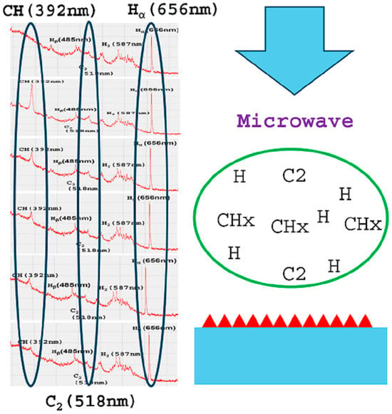
3.1. Optical Emission Spectroscopy Analysis
Table 1 lists peak wavelengths of OES signal intensity measured from microwave plasma for diamond deposition.
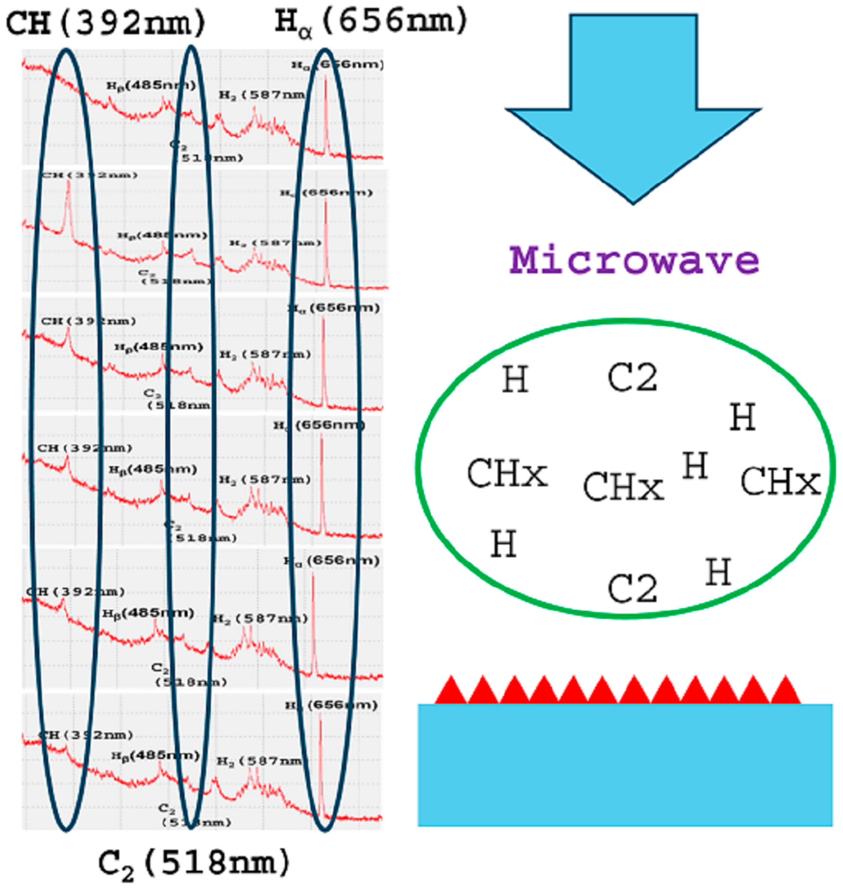
Figure 1 shows the OES of background light. The OES had peaks of 440 nm, 550 nm, and 625 nm.
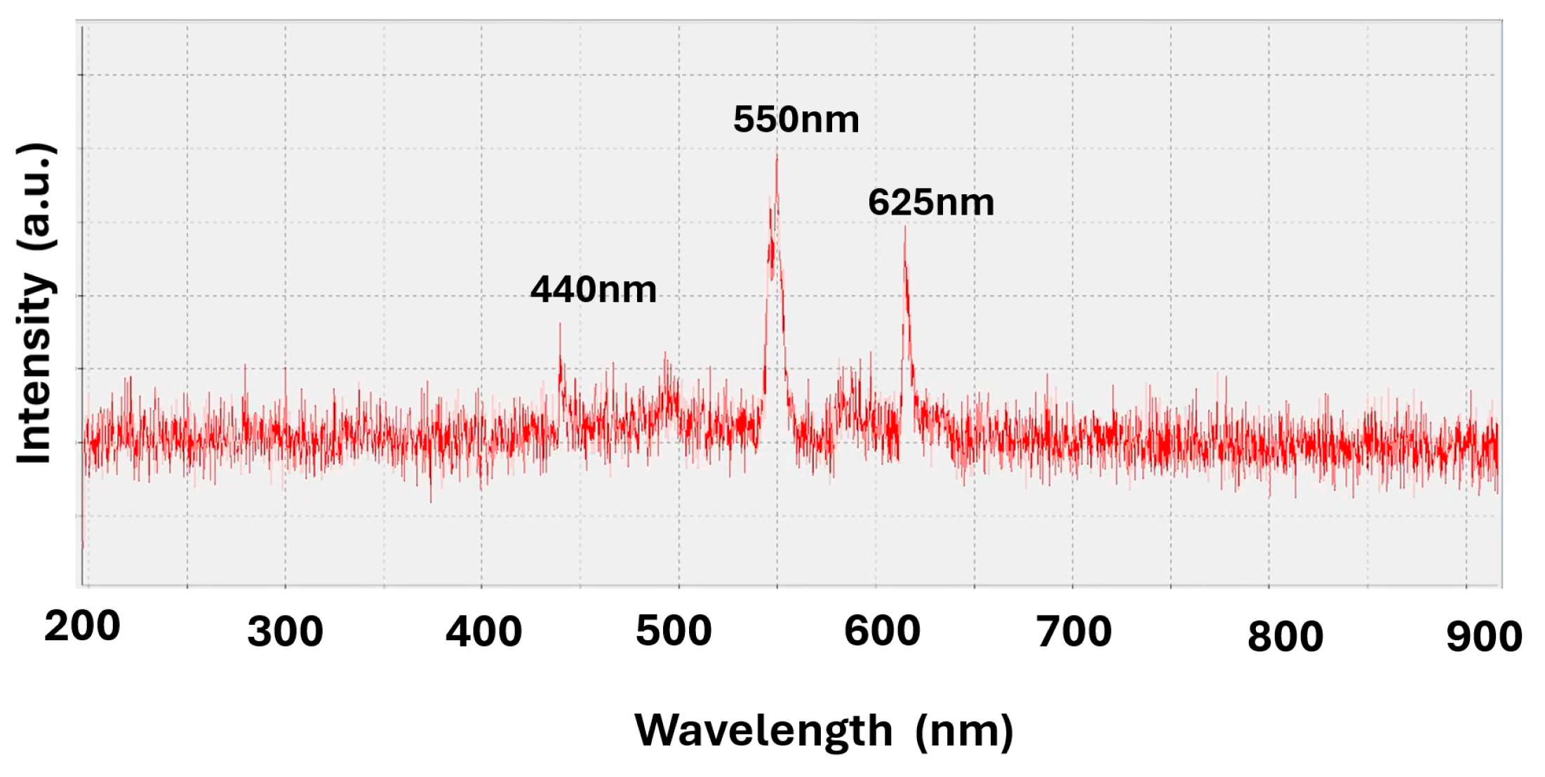
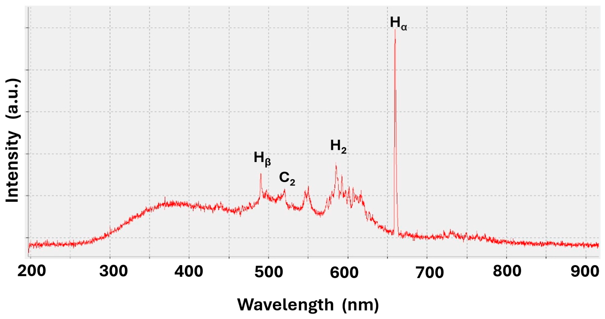
Figure 2 shows the OES of hydrogen plasma.
Figure 3 shows the OES of microwave plasma for diamond deposition in gas composition #2 without the addition of graphite paste. Using gas composition #1 (5% CH
4 and 1% CO
2 in H
2), 0.018 g graphite paste was applied to adhere silicon substrates onto a molybdenum plate. The molybdenum plate was then placed on a water-cooled substrate holder. After the hydrogen plasma was ignited and before CH
4 and CO
2 were fed to the plasma, a strong CH peak at 392 nm started to appear and reached the maximum intensity (at 1 min 30 s after hydrogen plasma was ignited) in the hydrogen plasma. After reaching the maximum intensity, the CH peak started to decrease gradually until it completely disappeared in about 10 min after the amount of graphite paste additive was diluted by the hydrogen gas flow. The CH peak disappeared after a longer time when more graphite paste was added. Peaks at 363 nm, 420 nm, and 518 nm also increased in intensity at the beginning of diamond deposition along with the CH peak at 392 nm. The peaks at 420 nm and 518 nm are attributed to CH and C
2, respectively. This shows that graphite paste dissociates in plasma and releases radicals and molecules, which are beneficial to the deposition of diamond film. Once all the graphite paste was dissociated and diluted by the hydrogen gas flow, the CH peaks at 392 nm disappeared. The C
2 peak remained longer into the next 20 min period for further deposition of diamond in CH
4 and H
2 gas flow with or without CO
2 additive.
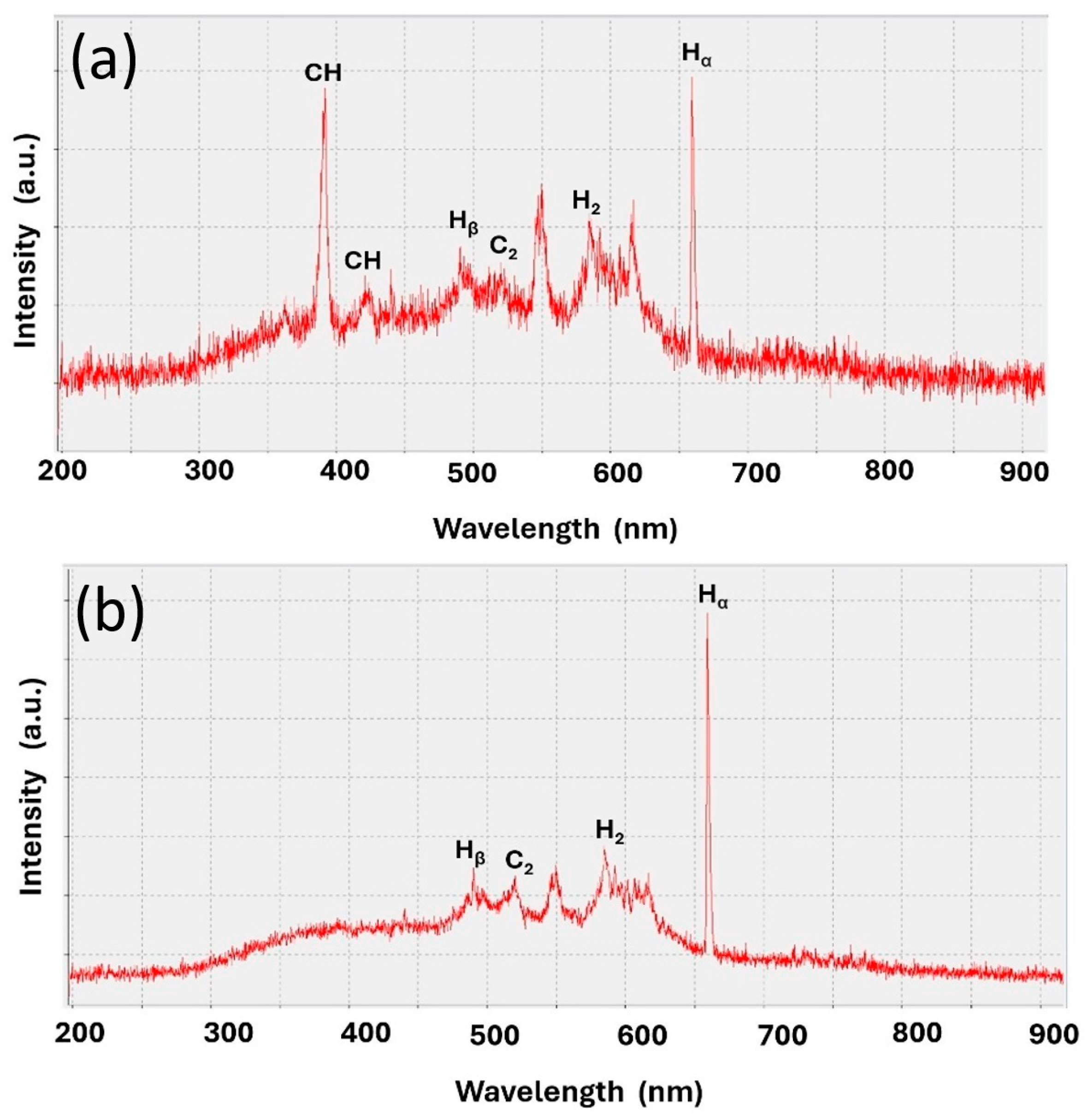
Figure 4a shows the OES when the CH peak reached the maximum intensity without CH
4 and CO
2. This was measured at 1 min 30 s after the plasma was ignited.
Figure 4b shows the OES of plasma in 5% CH
4 and 1% CO
2 balanced by hydrogen after the plasma was ignited for 20 min. Excluding the C
2 peak, other peaks attributed to graphite paste had completely disappeared.
The peaks at 440 nm, 550 nm, and 625 nm were from the background lights of the room, which existed before plasma was ignited. The peak at 550 nm should have been another peak attributed to C2, but the position overlapped with the background signals; thus, C2 was determined by the peak at 518 nm. The C2 peak at 518 nm showed a nearly constant intensity during the growth. OES peak positions of CH and CN overlapped at both 392 nm and 420 nm. For the experiments with graphite paste addition, there was a small peak at 363 nm. OES peak positions of CN and N2 overlapped at 363 nm. This indicated the possible existence of CN and N2 originating from the contents of the graphite paste.
Using gas composition #2 (5% CH4 in H2 without CO2 additive), 0.018 g of graphite paste was applied to adhere samples onto the molybdenum plate before placing the molybdenum plate on a water-cooled substrate holder for diamond growth. The diamond growth results using gas composition #2 were similar to those obtained using gas composition #1. The graphite paste appeared to dominate the diamond growth process, leading the difference between gas composition #1 and composition #2 to exhibit minor differences in the diamond growth results. After the hydrogen plasma was ignited and before CH4 was fed into the plasma, OES showed that the CH peak at 392 nm started to appear and reached the maximum intensity (at 1 min 10 s after hydrogen plasma was ignited) in the hydrogen plasma. After reaching the maximum intensity, the CH peak at 392 nm gradually decreased until it completely disappeared. The CH peak at 420 nm and C2 peak at 518 nm also increased in intensity along with the CH peak at 392 nm.
Once all the graphite paste was dissociated and diluted by gas feeds, the CH peaks at 392 nm and 420 nm disappeared, which also occurred approximately 10 min after the plasma was ignited. The C2 peak remained during diamond growth.
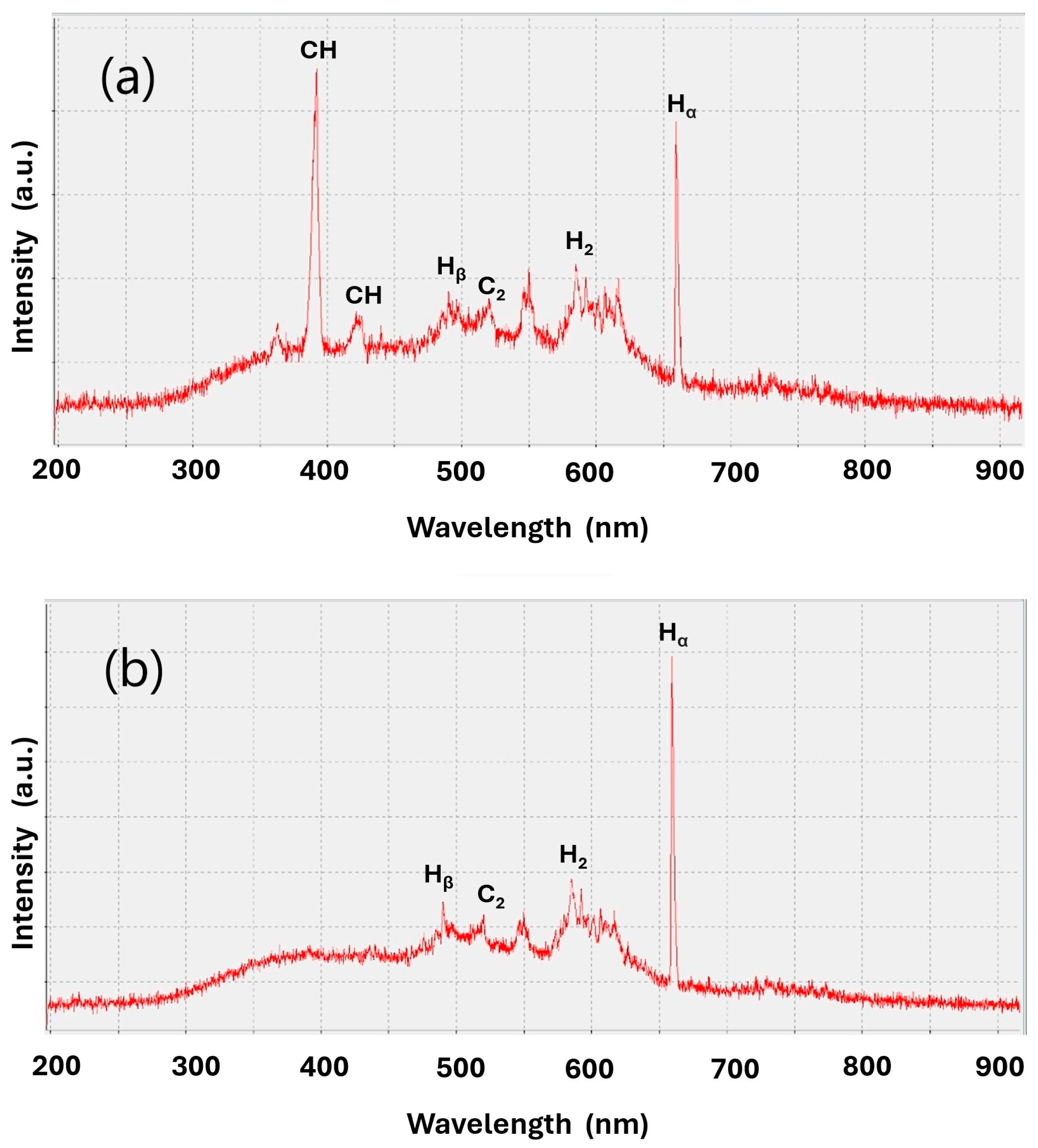
Figure 5a shows the OES of plasma with CH
4 additive when the CH peak reached the maximum intensity. It occurred at 1 min and 10 s after the plasma was ignited.
Figure 5b shows the OES of plasma in 5% CH
4 balanced by hydrogen at the time of 20 min after the ignition of the plasma. Besides the C
2 peak, the other peaks originated from graphite paste had completely disappeared. The C
2 peak at 518 nm showed a constant intensity during the growth. There was no apparent difference between the OES of the plasma in gas compositions #1 and #2, probably because the composition difference was only 1% CO
2 in the gas mixture.
In plasma with 5% CH4 balanced by H2 without the addition of graphite paste, OES did not show strong CH peaks at 392 nm and 420 nm nor the strong C2 peak at 518 nm. This confirms that strong CH peaks and C2 peaks can be attributed to the plasma dissociation of graphite paste. When 0.018 g graphite paste additive was applied, the effects of graphite paste took place during the first 10 min of diamond nucleation and growth. When more than 0.018 g graphite paste is added, the effects of graphite paste will last longer than 10 min.
3.2. SEM Analysis
SEM was employed to measure diamond grain size and film thickness. The graphite paste dissociated within about 20 min of the MPCVD process. To carry out diamond growth for a longer time under the influence of graphite paste, the substrate was taken out of the MPCVD chamber every 20 min to reapply the same amount of graphite paste. For the growth by MPCVD in gas compositions #1 and #2 with graphite paste additive, 0.018 g of graphite paste was reapplied between two consecutive 20 min growth periods. As a comparison, samples with a small amount of 0.008 g graphite paste applied only once before continuous 1 h growth were also obtained in gas compositions #1 and #2. These were further compared with diamond deposition without graphite paste additives.
3.2.1. Diamond Grain Size
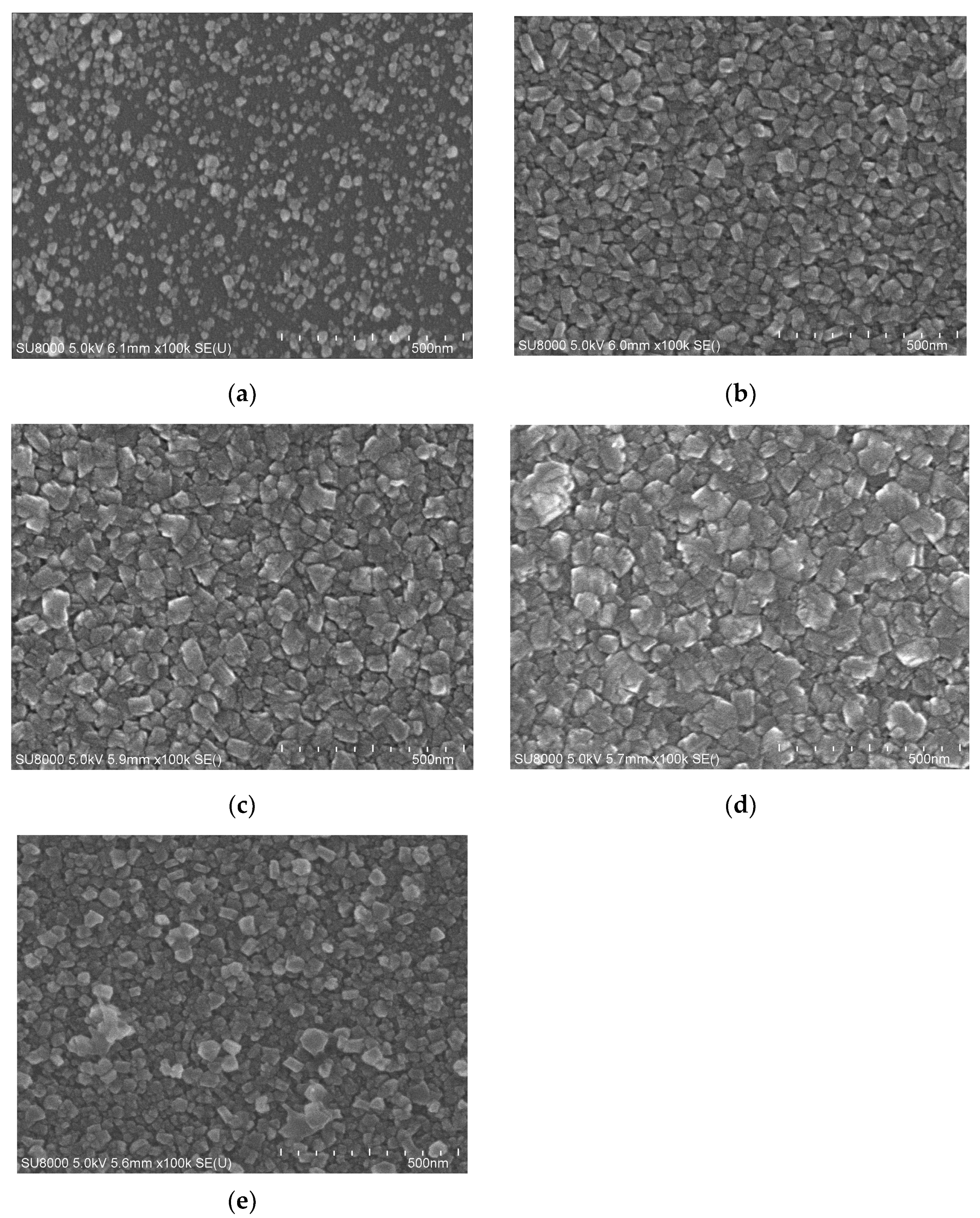
Table 2 shows a comparison of diamond grain sizes using gas composition #1 and gas composition #2. The average grain size for diamond films grown in gas composition #1 was 52.07 nm with standard deviation of 19.85 nm. The average grain size for diamond films grown in gas composition #2 was 53.25 nm with standard deviation of 19.52 nm. The similar results are attributed to the fact that although the gas compositions were slightly different, the amount of graphite paste additive, which dominated the diamond growth process, was the same for both cases.
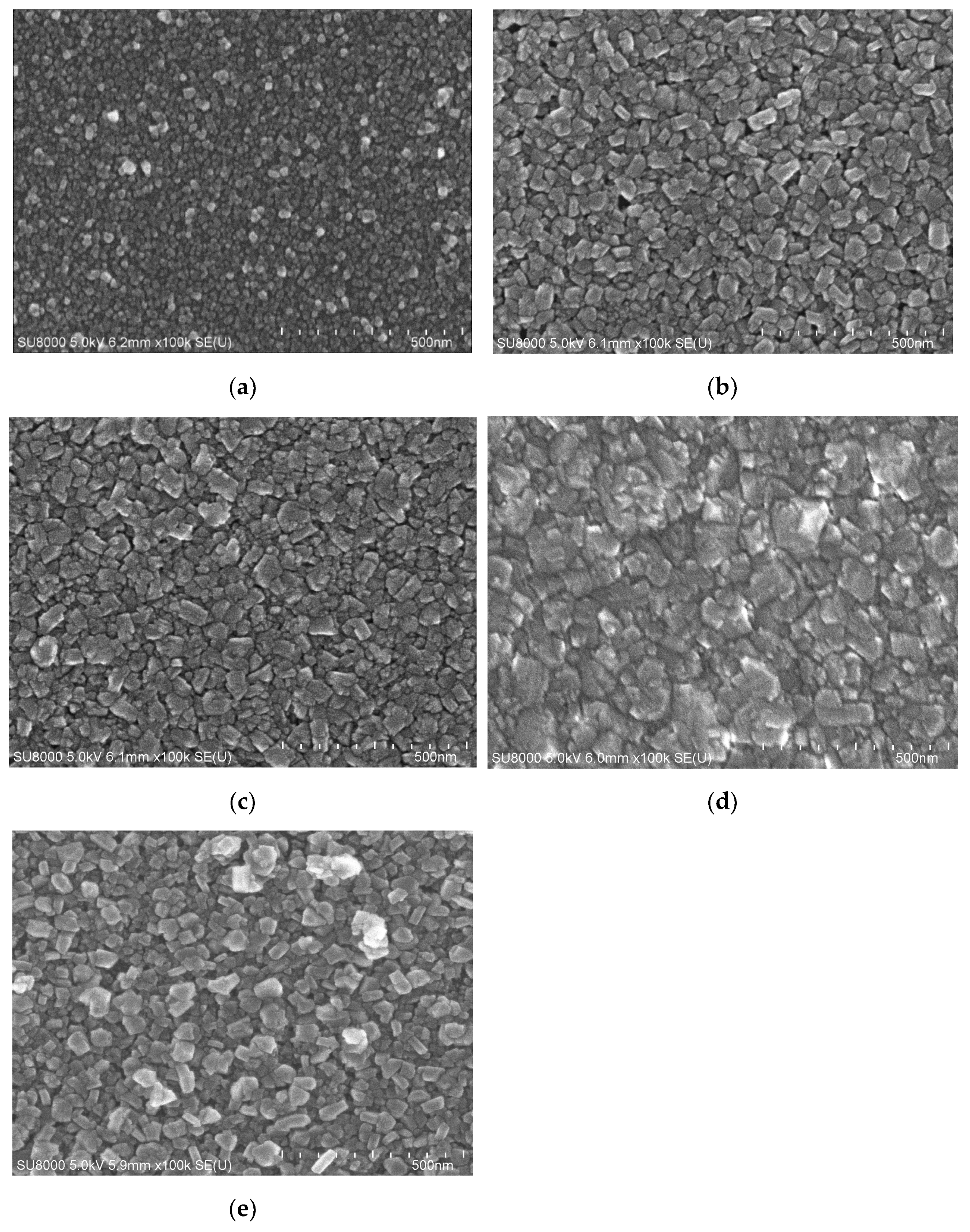
SEM plane-view images of diamond films grown in gas composition #1 are shown in
Figure 6, and SEM plane-view images of diamond films grown in gas composition #2 are shown in
Figure 7. Diamond films grown in gas compositions #1 and #2 without graphite paste additive exhibited an average grain size of 15–25 nm. The CO
2 additive resulted in a higher diamond nucleation density. When graphite paste was added, the diamond grain sizes were about 50 nm after the initial 20 min MPCVD process in both gas compositions #1 and #2. A strong OES peak from CH radical due to graphite paste additive promoted the growth rate of diamond grains from the 3 nm diamond seeds.
After terminating the initial 20 min MPCVD process for reapplying graphite paste followed by additional 20 min MPCVD process, the diamond grain sizes increased to about 65 nm. This process for reapplication of graphite paste was repeated again to grow diamond grains of about 80 nm in size. The growth rate with 0.018 g of graphite paste added for every 20 min resulted in the growth of diamond grain sizes by about 10–20 nm every 20 min. This trend was similar for both gas composition #1 and #2. This indicates the essential role of graphite paste additive in the growth of diamond at low temperatures.
Diamond grain sizes synthesized in 1 h continuous MPCVD were about the same as those produced by diamond MPCVD for only 20 min but with two times the amount of graphite paste additive. The importance of graphite pastes in the growth of diamond seeds to form diamond films at the substrate temperature around 450 °C was clearly demonstrated.
3.2.2. Diamond Film Thickness
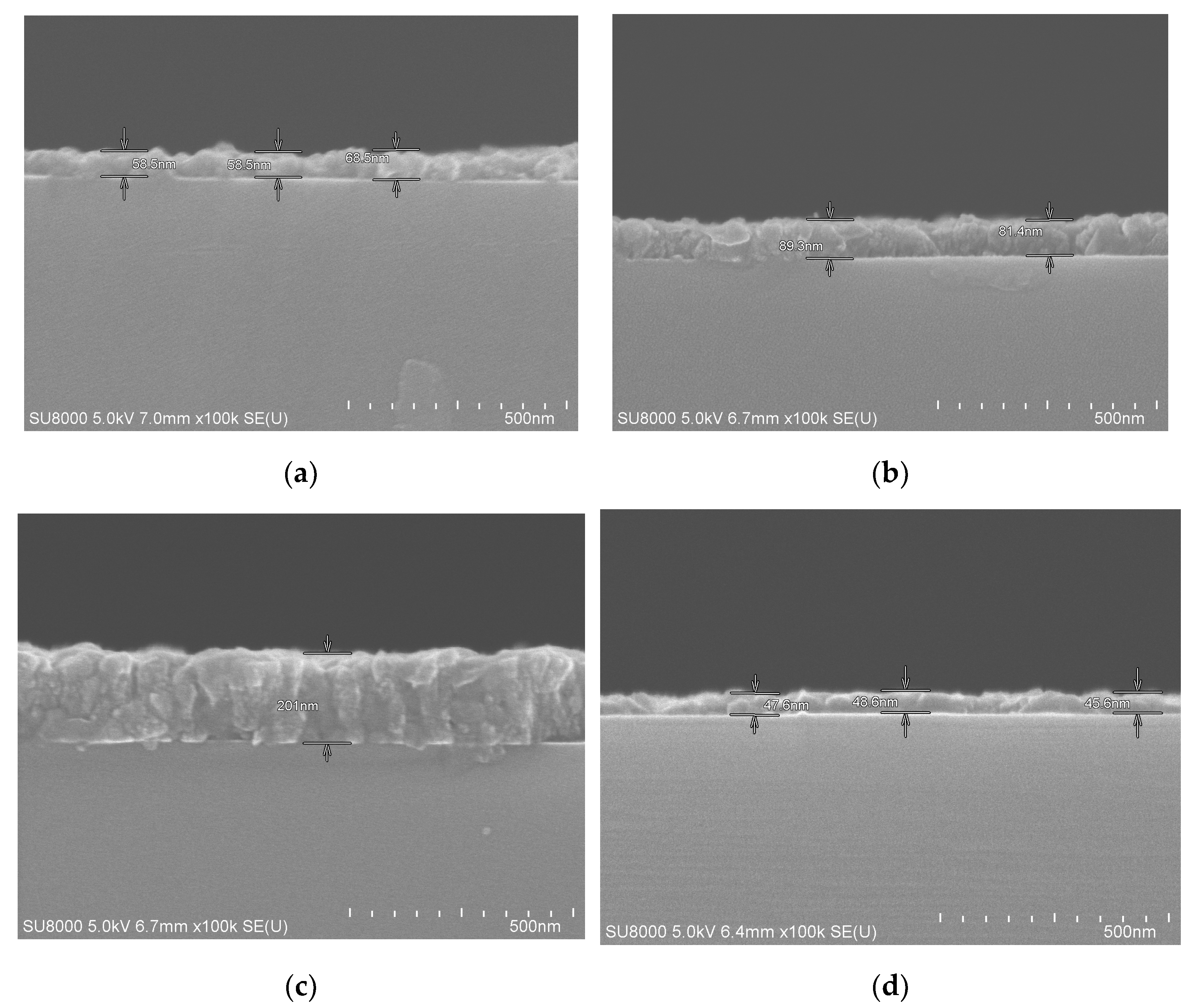
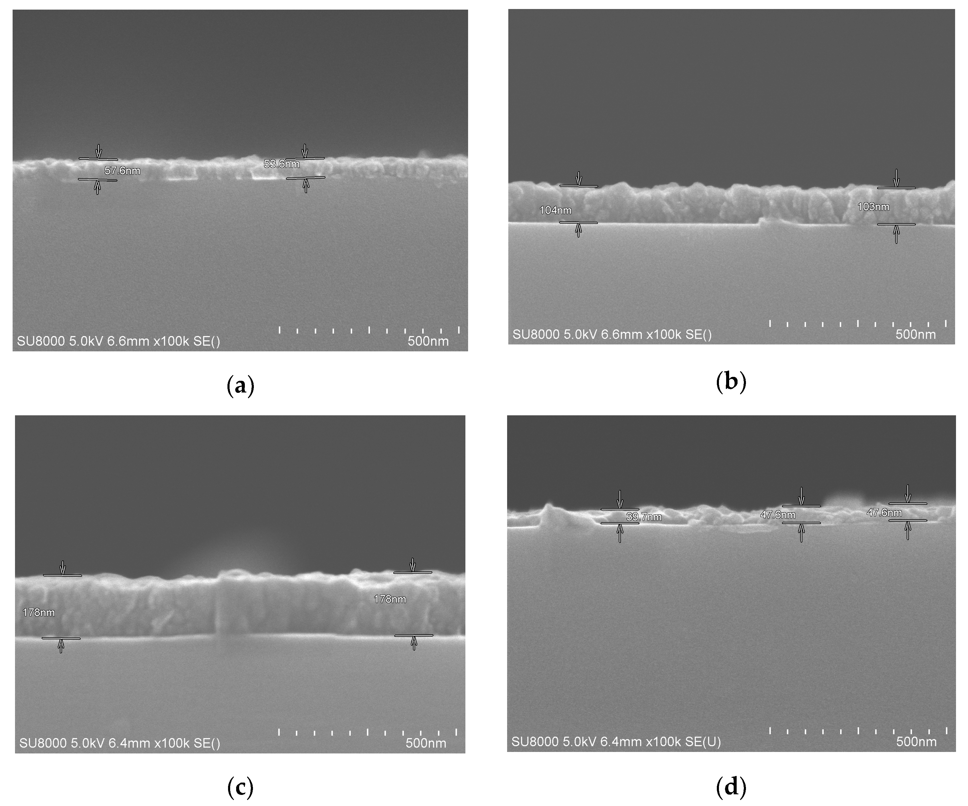
Table 3 shows a comparison of the thickness of diamond films grown under different conditions. The average thickness of diamond films grown in gas composition #1 was 97.88 nm with standard deviation of 58.82 nm. The average thickness of diamond films grown in gas composition #2 was 95.53 nm with standard deviation of 52.47 nm.
SEM cross-sectional-view images of diamond films grown in gas composition #1 are shown in
Figure 8, and SEM cross-sectional-view images of diamond films grown in gas composition #2 are shown in
Figure 9. The diamond films that grew continuously for 1 h with 0.008 g graphite paste additive were thinner than diamond films grown for 20 min with 0.018 g graphite paste. For both gas composition #1 and #2, the diamond films after 20 min growth with 0.018 g graphite paste had a thickness of about 60 nm. After two repetitive growth periods of 20 min each, the diamond film grown in gas composition #1 was 85 nm thick. As a comparison, the diamond film grown in gas composition #2 was 103.5 nm. After three repetitive growth periods of 20 min each, the diamond film grown in gas composition #1 was 197 nm. As a comparison, diamond films grown in gas composition #2 were 178 nm. In repetitive 20 min growth periods with graphite paste being applied in each growth period, diamond films of nearly 200 nm were deposited within 1 h at a low temperature around 450 °C. In contrast, the diamond film grown for 20 min without graphite paste was too thin for the measurement of the thickness by SEM.
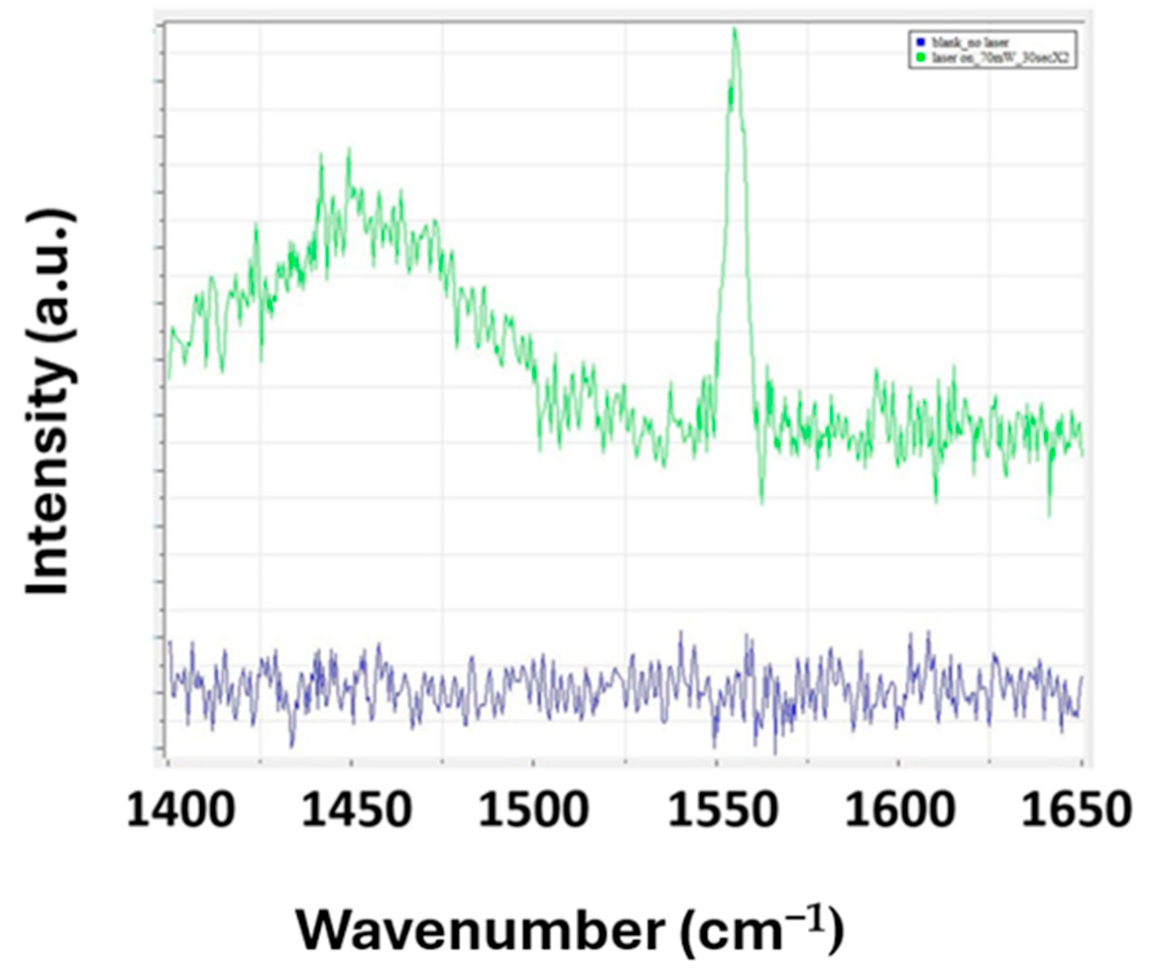
3.3. Raman Spectroscopy Analysis
Raman spectroscopy excited by a 458 nm light source was employed to characterize diamond films. Relevant Raman peak positions are listed in
Table 4. The peaks at 1445 cm
−1 and 1556 cm
−1 were background Raman scattering signals attributed to the quartz optical components excited by the 458 nm laser, as shown in
Figure 10. Raman spectra for diamond films grown in gas composition #1 are shown in
Figure 11 and
Figure 12, while Raman spectra for diamond films grown in gas composition #2 are shown in
Figure 13 and
Figure 14.
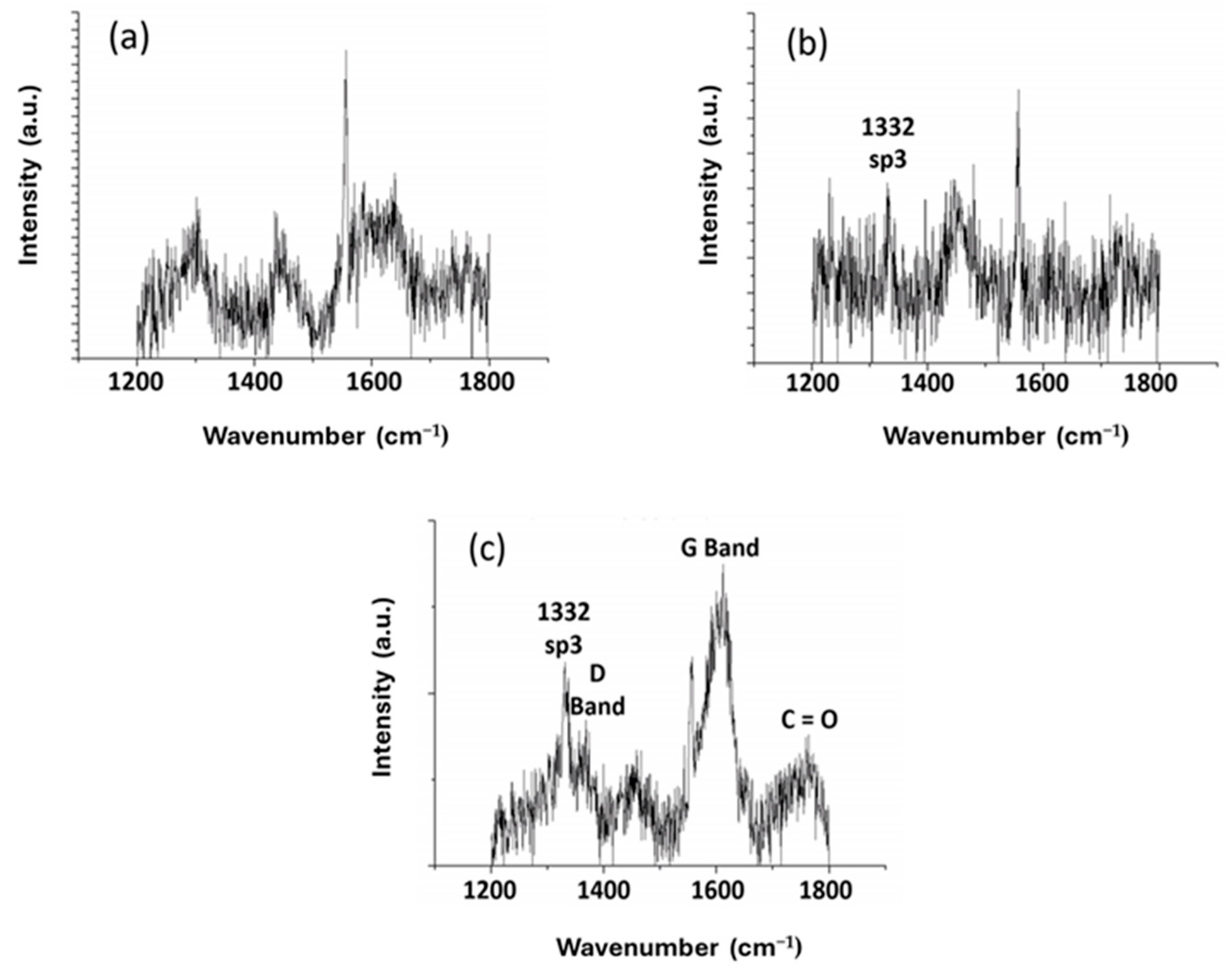
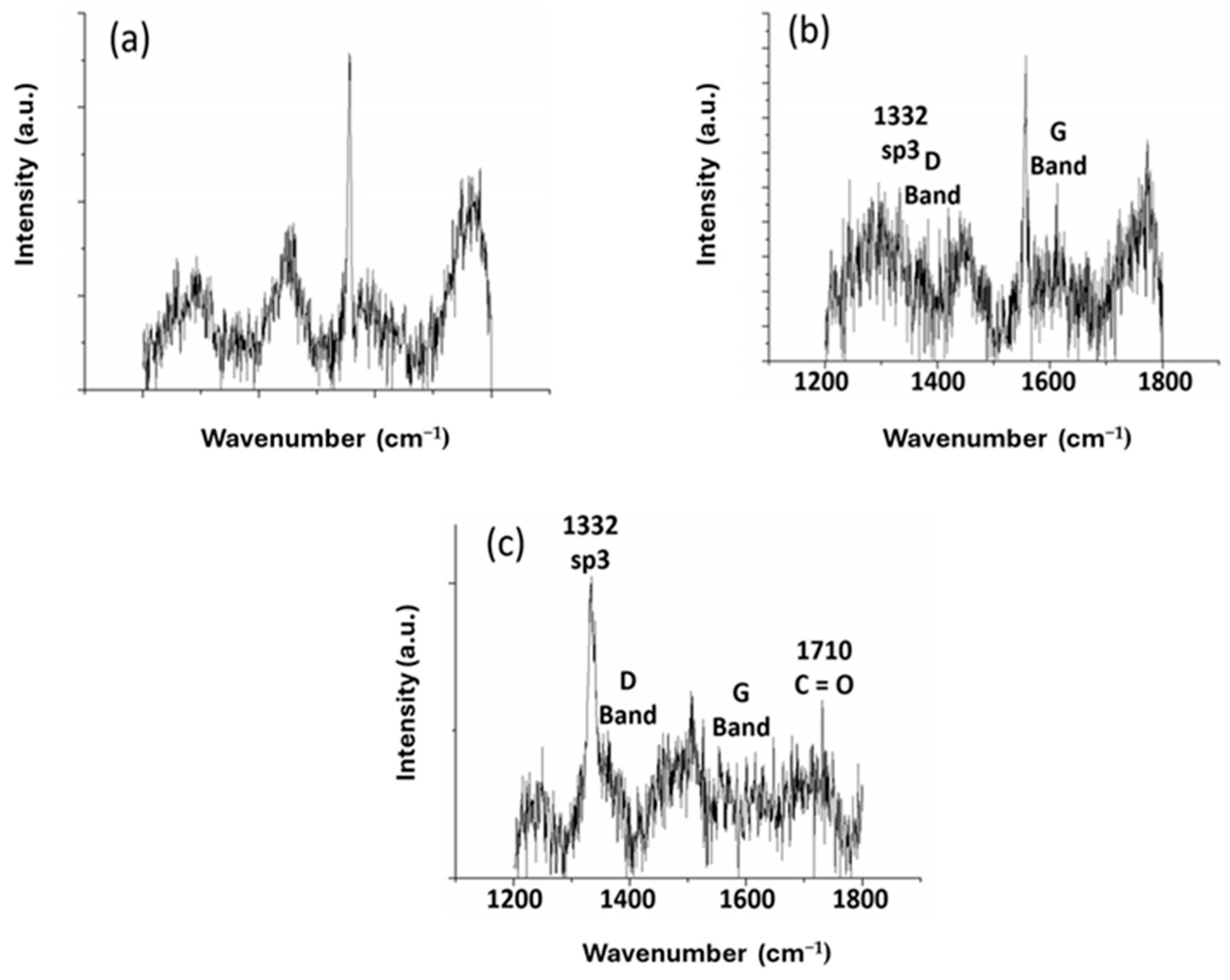
For both gas compositions, Raman spectra of diamond films grown for 20 min without graphite paste did not display the diamond peak at 1332 cm
−1, as shown in
Figure 11 and
Figure 13a. However, those for the diamond films grown with graphite paste additive displayed the diamond peak at 1332 cm
−1 after 20 min diamond growth. The addition of graphite paste to the MPCVD process contributes to the formation of sp
3-bonded diamond.
Diamond films grown for 20 min in gas composition #1 with a small amount of 0.003 g graphite paste additive did not display the D band and the G band. When a larger amount of 0.018 g graphite paste was added, the D band and G band appeared, as shown in
Figure 11.
Diamond films grown for 20 min in gas composition #2 with 0.0045 g graphite paste additive displayed the D band and G band after 20 min diamond growth, as shown in
Figure 13b. In comparison with diamond films grown in gas composition #1, diamond films grown in gas composition #2 with 0.018 g graphite paste also displayed the D band and the G band Raman signal, as shown in
Figure 13.
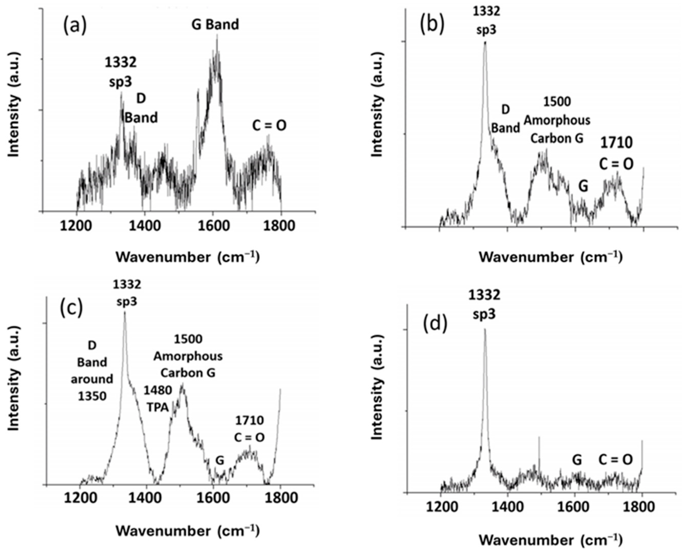
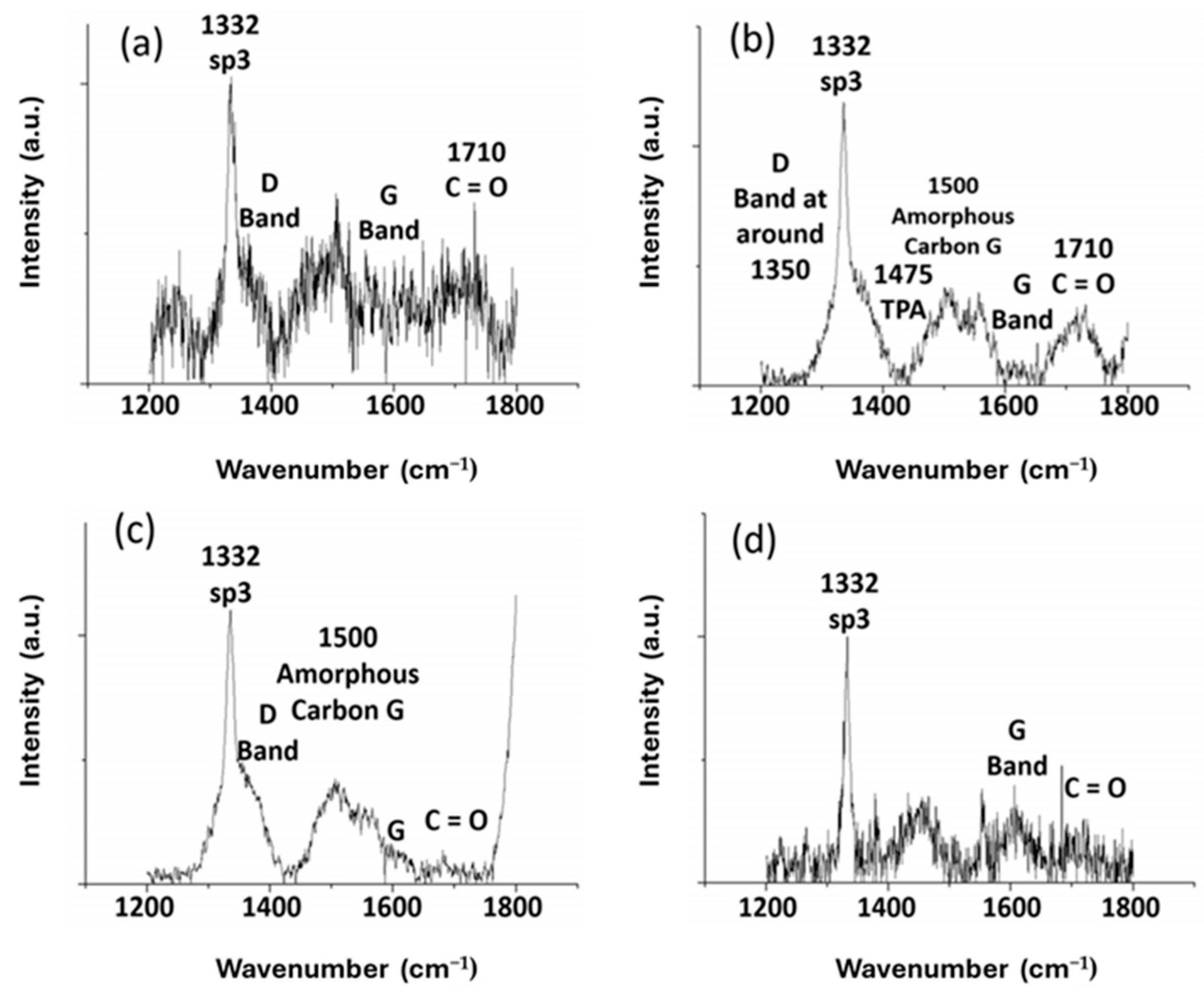
From the comparison between
Figure 12d and
Figure 14d, diamond films grown for 1 h continuously with 0.008 g graphite paste added at the beginning displayed the G band signal, but the D band signal disappeared. This revealed that when too little (0.008 g) graphite paste was added, the D band Raman signal disappeared after a 1 h growth process.
Figure 12 and
Figure 14 show that Raman scattering of diamond films grown by the repetitive termination of the growth process for additional graphite paste additive displayed the sp3 diamond Raman peak. A larger amount of graphite paste contributed to the formation of sp3-bonded diamond along with more intense G bands and D bands. However, Raman spectra for diamond films grown by two-time and three-time repetitive growth processes with graphite paste additives showed that the G band signal strength at 1600 cm
−1 decreased, and the Raman scattering from TPA and amorphous carbon at 1500 cm
−1 became more apparent. Diamond films grown in both gas composition #1 and #2 displayed Raman scattering from TPA at diamond grain boundaries.
Raman spectra of repetitive 20 min growth of diamond films for a total of 1 h with resupply of graphite paste at 0.018 g for each period were compared with those of diamond films grown continuously for 1 h with 0.008 g graphite paste added only once at the beginning. Raman spectra for diamond grown by the repetitive process with resupply of 0.008 g graphite paste each time displayed Raman peaks of G-band and D band at 1500 cm−1, while the diamond films grown by continuous process with graphite paste supplied only once at the beginning displayed only the G band without the D band.
Except for the small difference between diamond films grown for 20 min in gas composition #1 with 0.003 g graphite paste additive and those grown in gas composition #2 with 0.0045 g graphite paste additive in growth condition 1 and 0.0045 g growth with growth condition 2 for 20 min, no significant difference was observed between diamond films grown in two different gas compositions. Significant differences in diamond film characteristics were observed when the amount of graphite paste additive varied. Graphite paste affected diamond growth at low temperature more than the 1% CO2 additive in both gas compositions.
The application of an oxy-hydrocarbon vapor such as acetone with CO
2 and O
2 additives for MPCVD growth of diamond was reported at temperatures between 600 °C and 1400 °C higher than those in this work [
26]. After fine-tuning the percentage of C, H, and O in the gas mixture, Bachmann et al. [
2] summarized the growth zone in the C, H, and O phase diagram. Effects of substrate temperature on diamond growth in the low-temperature range of 450 °C were not clearly understood. Nevertheless, desorption or abstraction of atomic hydrogen termination on the diamond growing surface was seen as desirable in order to create active carbon sites for the attachment of carbon-containing radicals. Oxygen was expected to play a role in activating the diamond growing surface to promote the diamond growth rate. An appropriate amount of oxygen was seen as beneficial to diamond growth at low temperature, which is consistent with results presented in this work.
Nanoscale graphite was reported to be beneficial for diamond growth. For example, Li et al. applied highly oriented pyrolytic graphite (HOPG), and graphite fibers as precursors to promote diamond deposition on graphite-seeded silicon wafers. They reported that the number density of diamond nuclei was enhanced by the presence of graphite, and that diamond grew preferentially on the prism planes of graphite,; i.e., on the edges of graphite. There was an epitaxial relationship between graphite and diamond. There was etching of graphite when diamond was nucleated [
27]. Xie et al. performed simulation work and suggested that graphite preferentially turned into hexagonal diamond instead of cubic diamond [
28]. Lambrecht et al. performed calculations and suggested that diamond can nucleate on graphite with subsequent hydrogenation along the edges of graphite [
29]. In this work, the graphite paste included nanoscale graphite as a conductivity additive. It was thought that some of the nanographite was released into the plasma along with the vaporized solvent and binder of the graphite paste. Hydrogen and oxygen would react with nanoscale graphite to form carbon-containing radicals, which help promote the diamond growth. The latter research is consistent with the experimental results presented in this work demonstrating the dominating effects of graphite paste in the growth of diamond.
We observed that graphite paste contributed to the growth of sp3 bonded carbon. Too much graphite paste additive also contributed to the formation of Raman scattering of the D band and G band signal. The effects of graphite paste added to the MPCVD of diamond films at a low temperature of 450 °C have been revealed to significantly enhance the diamond growth rate from the beginning of the deposition process. This promotion converts the undesirable small-diamond-grain diamond films, which suffer from frequent phonon scattering at the abundant grain boundaries, into large-diamond-grain diamond films beginning from the silicon-diamond interface. Optimization of the thermal conductivity, dielectric strength, leakage current, and mechanical strength of low-temperature diamond films deposited by this novel process is being carried out. Preliminary results indicate high thermal conductivity of the low-temperature diamond films of several tens to a few hundred nanometers thick are feasible. Detailed results will be published elsewhere in near future.
4. Conclusions
A novel MPCVD process, leading to enhanced growth rate, grain size, and sp3/sp2 ratio for nano-diamond thin films on silicon, was demonstrated. Graphite paste containing nano-scale graphite, an oxy-hydrocarbon binder, and solvent vaporized and mixed with gas feeds of hydrogen, methane, and carbon dioxide to form plasma. Rapid grain growth from 3 nm diamond seeds embedded on silicon resulted in the growth of diamond films with large diamond grains on the nucleation side at a rate exceeding 200 nm/h at around 450 °C. Quantitative study on the effects of the graphite paste additive on low-temperature diamond deposition was carried out and reported based on SEM, Raman scattering of diamond films, and OES analysis of the plasma chemistry. As a comparison, without the graphite paste additive, the diamond growth rate and diamond grain size were impractically small. This novel process helps make diamond a more promising dielectric material for future IC fabrication in the semiconductor industry. Optimization of the thermal conductivity, dielectric strength, leakage current, and mechanical strength of low-temperature diamond films synthesized by this novel process is being carried out and will be reported elsewhere.


