Article

Bipolar Nb3Cl8 Field Effect Transistors

1
School of physics, Dalian University of Technology, Dalian 116081, China
2
State Key Laboratory of Quantum Optics and Quantum Optics Devices, Institute of Optoelectronics, Shanxi University, Taiyuan 030006, China
3
Collaborative Innovation Center of Extreme Optics, Shanxi University, Taiyuan 030006, China
4
Hefei National Laboratory, Hefei 230088, China
*
Author to whom correspondence should be addressed.
Magnetochemistry 2024, 10(6), 43; https://doi.org/10.3390/magnetochemistry10060043
Submission received: 26 April 2024 / Revised: 31 May 2024 / Accepted: 11 June 2024 / Published: 14 June 2024
(This article belongs to the Special Issue Advances in Magnetic Two Dimensional Materials)

Abstract

:
Field effect transistors based on few-layered van der Waals transition metal halide (TMH) Nb3Cl8 are studied in this work. Few-layered Nb3Cl8 exhibits typical N-type semiconducting behavior controlled by a Si gate, with the electrical signal enhancing as the thickness increases from 4.21 nm to 16.7 nm. Moreover, we find that the tunability of few-layered Nb3Cl8 FETs’ electrical transport properties can be significantly augmented through the use of an ionic liquid gate (or electrical double layer, EDL). This enhancement leads to a substantial increase in the on–off ratio by approximately a factor of 10 2 , with the transfer curve modulated into a bipolar fashion. The emergence of such bipolar tunable characteristics in Nb3Cl8 FETs serves to enrich the electronic properties within the transition metal halide family, positioning Nb3Cl8 as a promising candidate for diverse applications spanning transistors, logic circuits, neuromorphic computing and spintronics.

1. Introduction

Inspired by the exfoliation of graphene, the low-dimensional materials especially the two-dimensional (2D) van der Waals (vdW) materials have gained great attention due to their natural atomically thin structure, large surface-to-volume ratio, diverse properties, high carrier mobility, mechanical flexibility, heterostructure engineering capabilities, and environmental stability, promoting to unveil emerging physical phenomena, such as quantum Hall effect [1], fractional quantum Hall effect [2], strong correlation properties [3], catalytic performance [4], optoelectronic performance [5], high thermal conductivity [6], etc. These remarkable attributes make them highly promising for various applications in electronics, optoelectronics, energy storage, sensors, and beyond [7,8,9,10,11,12]. Since then, 2D semiconductors, such as transition metal dichalcogenides (TMDC) [13,14,15] and transition metal halogens (TMHs) [16,17], dominated by interlayer weak van der Waals interaction have been extensively investigated. Compared to TMDC materials, TMH materials exhibit more attractive advantages due to their richer magnetic and topological properties [18,19].
Nb3Cl8, as a member of vdW TMHs, is believed to be mechanically exfoliated, with an interlayer cleavage energy of 0.18 Jm 2 [20]. Recent study has confirmed the existence of a breathing Kagome lattice in Nb3Cl8, which could open a band gap at the Dirac point due to the spatial inversion symmetry being broken [21]. Due to Nb3Cl8’s structural characteristics, it has also been predicted to manifest quantum spin liquid owing to magnetic frustration [22], yielding a topological flat band (TFB) because of its inherent mirror symmetry. The TFB is then confirmed by using the angle-resolved-photon-energy-spectroscopy (ARPES) with a band gap around 1.12 eV [21]. The magnetic ground state of single layer Nb3Cl8 has also been reported recently [21]. Nb3Cl8, a material that can be mechanical exfoliated down to a single layer, possesses a suitable bandgap as a semiconductor, holds the promise for the low-dimensional material field-effect transistors (FETs), and exhibits strong electrostatic control. With its stability at room temperature, non-toxic nature, and other characteristics, Nb3Cl8 is considered a highly promising electronic system for studying electrical transport performance [20]. Recently, attempts have been devoted to probe the electrical properties of few-layered Nb3Cl8, which is encapsulated by hexagonal-boron nitride (h-BN) [23] and O2 adatoms [24], respectively. However, the reported on–off ratio of Nb3Cl8 based FETs is around 10 0 , which greatly limits its application in electronic devices. Therefore, it is imperative and necessary to investigate effective tuning methods to enhance the on–off ratio and enrich the electrical transport characteristics of Nb3Cl8-based FETs.
In this work, we employ the mechanical exfoliation method to obtain high-quality few-layered Nb3Cl8 nanoflakes and fabricate FETs based on few-layered Nb3Cl8 with different thicknesses. Systematic studies are conducted on the electrical properties for few-layered Nb3Cl8 FETs equipped with Si and EDL gates, respectively. Our results show a N-type doping and on–off ratio of 10 0 with Si gate FETs, while the devices exhibit bipolar doping effects and on–off ratio over 10 2 with EDL gates. Our work could shed light on the future investigation on nano-electronic devices based on Nb3Cl8.

2. Methods

2.1. Manufacture and Testing of FETs

We employ mechanical exfoliation to obtain few-layered Nb3Cl8 from high-quality bulk Nb3Cl8. Nb3Cl8 nanoflakes are then deposited on SiO2 (300 nm)/Si++ substrate. Morphology and thickness of few-layered Nb3Cl8 are characterized by optical microscopy and atomic force microscopy (AFM) [25]. Then, we further study its stability upon heating and organic solvent compatibility (acetone and isopropanol) for following fabrications. It reveals that heating could cause degradation of Nb3Cl8. Therefore, we avoid using any heating step for the whole fabrication process, such as the BN-encapsulated process. Next, we fabricate the contact electrode of the Ti5 nm/Au50 nm film by using the electron beam lithography and electron beam evaporation. Finally, we use a semiconductor analyzer (Keysight B1500a) to measure the field effect curves and I-V curves of the as-prepared Nb3Cl8 devices.

2.2. Ionic Liquid Gating Method

We use the ionic liquid N,N-diethyl-N-methyl-N-(2-methoxyethyl) ammonium bis (trifluoromethylsulfonyl) imide (DEME-TFSI) as a gate on the Nb3Cl8 surface to create an EDL. It exhibits great modulation compared with conventional solid dielectric materials [26,27]. A droplet of DEME-TFSI is deposited to cover both the device channel and the gate pads, after which the entire area is covered with a thin glass lid for observation under the microscope [28].

2.3. Raman Spectra

Raman spectra are acquired for both bulk and few-layered Nb3Cl8 using a 532 nm excitation source. The experiments to investigate the layer-dependent Raman behavior are conducted using a confocal microscope Raman spectrometer (LabRAM HR Evolution, Horiba Scientific, Raman detector, Lille, France) in a backscattering geometry. The emitted Raman signals are collected and dispersed by a 1800 gr/mm grating, with a 532 nm laser serving as the excitation source. The laser beam was focused onto exfoliated Nb3Cl8 flakes using a 100× objective (NA = 0.9, WD = 0.21 mm), resulting in a spot size of approximately 1 μ m. Each Raman spectrum was obtained by averaging ten measurements, with an integration time of 2 s for each spectrum.

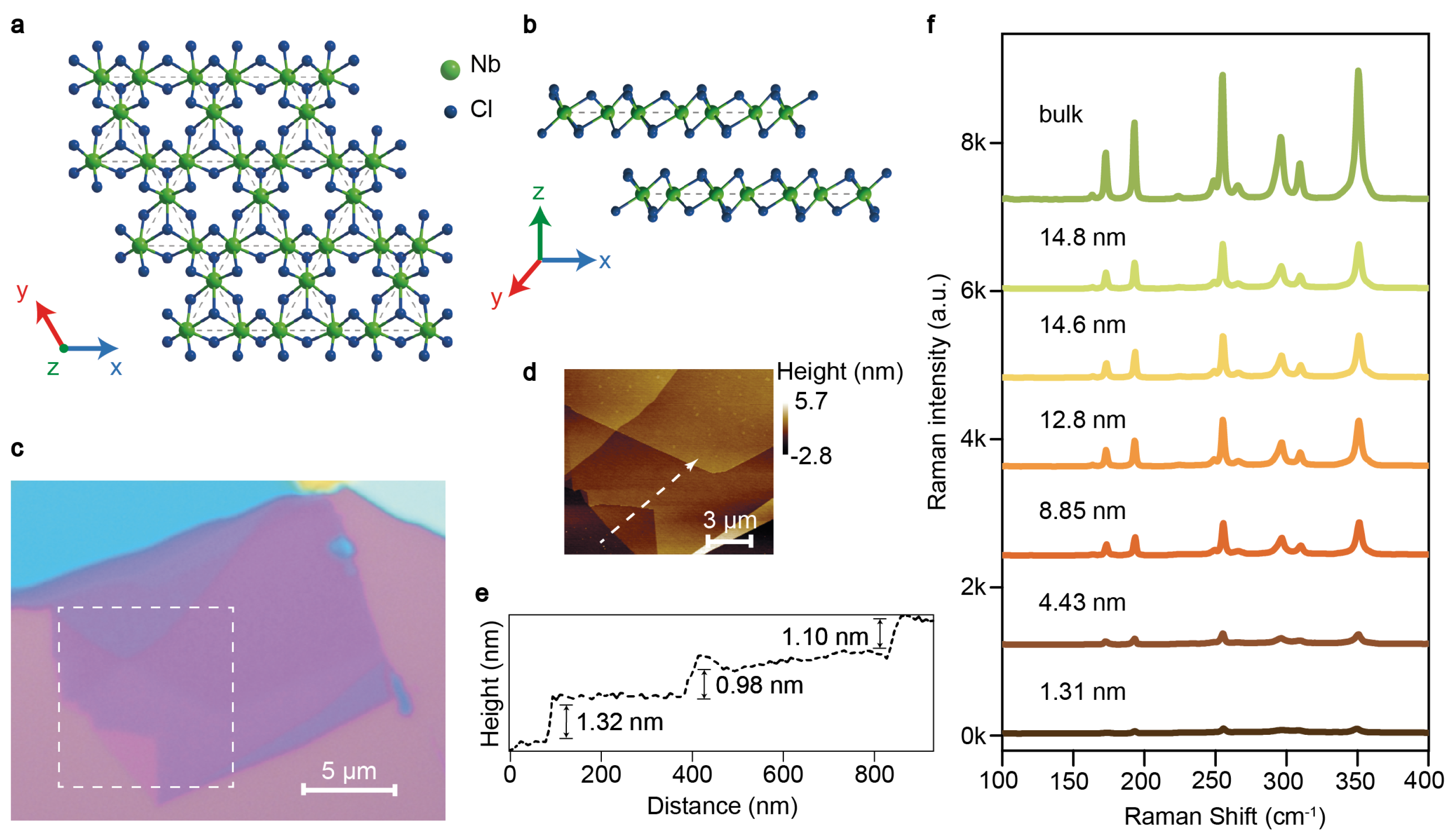
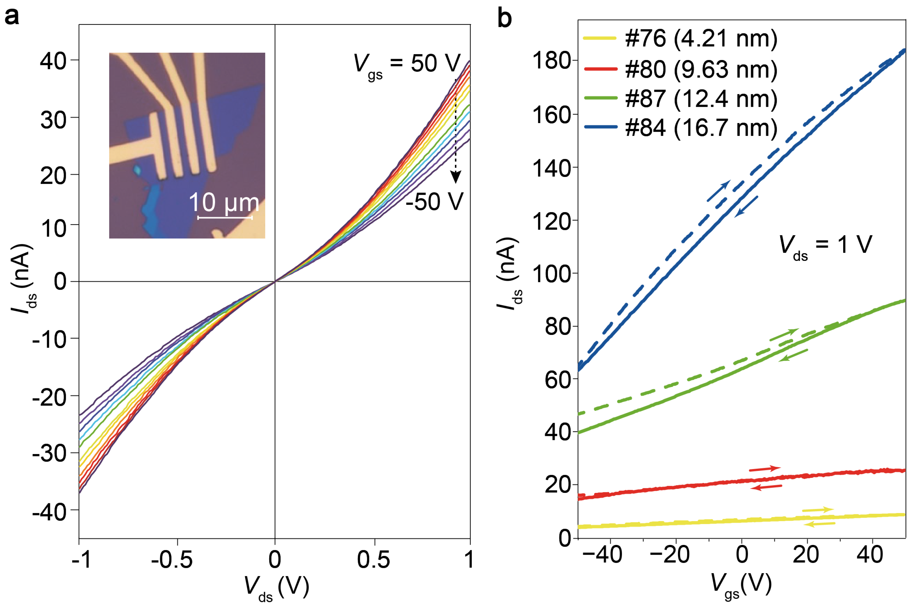
3. Results and Discussion

Figure 1a,b show the ball-and-stick schematic diagram of the Nb3Cl8 at the top and side views. The green and blue balls represent Nb and Cl atoms, respectively. The structure belongs to the space group P 3 m ¯ 1. The gray dash lines identify the trimer clusters combined by Nb atoms. The short distance between Nb-Nb is d1 = 2.8 Å and the long one is d2 = 3.9 Å. The large trimer clusters and the small ones alternative arrangement forms the breathing Kagome lattice. The optical microscopy image of a typical exfoliated multi-layered Nb3Cl8 is shown in Figure 1c, where we can see clearly the optical contrast between different layers. AFM scanning helps us to confirm the height difference between layers, where the thinnest part is detected to be about 1.3 nm with about two layers. Therefore, the 2D van der Waals nature is confirmed by both optical microscopy and AFM.
I-V curves of a typical thin-layer Nb3Cl8 device with gate voltage varying from −50 to 50 V are shown in Figure 2a, while its optical microscopy image is shown in the inset. Non-linear I-V curves are obtained by varying the drain voltage in between ±1 V, which means a non-ohmic contact is formed between Nb3Cl8 and electrodes. By increasing the gate voltage gradually from −50 to +50 V, the absolute value of I d s is increasing. Fixing the V d s constantly at +1 V, by changing Si gate voltage from −50 to +50 V gradually, the field-effect curves are obtained and shown in Figure 2b. Combing transfer curves shown in Figure 1a,b, the intrinsic N-type semiconductor of thin-layer Nb3Cl8 device can be confirmed, which is consistent with the previous work [24]. Compared with the transfer curves for devices at different thickness in Figure 2b, we can find that increasing thickness of Nb3Cl8 could play a positive role to give rise to I d s . This phenomenon could be attributed to an improved contact and/or a channel conductivity enhancement. The field-effect curves exhibit similar trends for each thickness devices, and the on-off ratio is approximately consistent. This indicates that the electrical modulation of the material remains relatively stable across the range of thicknesses from 4.21 to 16.7 nm tested in this experiment.
Non-linear I-V behavior in Figure 2a indicates that there may exist a high contact resistance between the Nb3Cl8 thin layer and the Ti/Au electrodes. This resistance could impede the Si gate’s modulation to the sample’s intrinsic carriers. Therefore, we measure the resistance between the two middle electrodes using both two-probe and four-probe methods. As shown in Figure 3a, the two-probe measurement shows a non-linear I-V curve and a changing resistance with different V d s due to the Schottky barrier between the electrode and the Nb3Cl8 channel. The red curve in Figure 3a shows that the total resistance ( R t o t = d V d s /d I d s ) is about 25 M Ω , which is composed of the Nb3Cl8 channel resistance ( R c h ) and the contact resistance ( R c ). Then, we select a safe input current range from −20 to 20 nA for the four-probe measurement, preventing an excessive voltage causing the device breakdown. A linear V-I curve and a stable resistance in Figure 3b shows that the channel intrinsic resistance ( R c = d V 23 /d I 14 ) of Nb3Cl8 is about 14 M Ω . The contact resistance ( R c ) is then calculated to be about 10 M Ω , which is of the same order as the channel resistance. Therefore, resistance obtained by the four-probe method compared to the two-probe method (Figure 3c) demonstrates a more accurate field effect of the Nb3Cl8 flake.
Since the limited tuning effect of the solid Si gate, we then turn to a stronger tuning method by using the ionic liquid to create a non-volatile but hygroscopic EDL [29]. A field effect transistor with 16.7 nm Nb3Cl8 is prepared here for ionic liquid tuning. The transistor’s optical image and schematic diagram are shown in Figure 4a,b. The transfer curves under ionic liquid with different V d s are shown in Figure 4c, which exhibits a stronger tuning effect compared with solid Si gate shown in Figure 2b. Without external doping, the Nb3Cl8 exhibits an intrinsic N-type semiconductor, which is consistent with the results shown in Figure 2b. Tuned by the ionic liquid, Nb3Cl8 shows bipolar semiconductor characters, where the dominated carrier type could be changed by varying the voltage applied on the ionic liquid. Take the transfer curve at V d s = 0.1 V, for example, when the gate voltage applied on the ionic liquid increases from −0.7 to 1.5 V, negative carriers (electrons) accumulates in Nb3Cl8 channel and I d s increases responsively, showing a N-type field effect. When the gate voltage decreases from −0.7 to −1.5 V, positive carriers (holes) take in charge, showing a P-type field effect. Besides the bipolar FET characters, the on–off ratio could be further enlarged by a factor of 10 2 compared with the solid Si gated FET, which conforms again the strong doping ability of EDL. The corresponding I d s could be further increased by increasing the V d s , which can be observed obviously in Figure 4c. The bipolar characters and enhanced on–off ratio under EDL are further conformed by checking additional FETs with varying thickness (12.4 and 6.08 nm) of Nb3Cl8.

4. Conclusions

By using the mechanical exfoliation method, the high-quality few-layered TMH material Nb3Cl8 is acquired. Systemically electronic properties are studied by fabricating the Nb3Cl8-based FETs. By applying the solid Si gate and ionic liquid doping methods, the intrinsic N-type semiconductor characters are discovered. Furthermore, the implementation of the ionic liquid results in the formation of an electric double layer at the surface of the Nb3Cl8 channel, inducing the bipolar characteristics in Nb3Cl8-based FETs. This enhancement is evidenced by the significant increase in the on–off ratio, rising from approximately 10 0 with Si gating to around 10 2 with ionic liquid tuning. The effectiveness of our ionic liquid in achieving this tuning effect was further verified by examining Nb3Cl8 FETs with varying thicknesses. Considering the reported electronic performances and light absorption properties, our findings present new possibilities for future electronic studies involving Nb3Cl8. Moreover, these results may provide valuable insights that can be extrapolated to other TMH materials.

Author Contributions

Y.L., B.D., K.Z. and T.Z. conceived the research; Y.L. exfoliated sample and fabricated FETs; Y.L. and T.Z. measured the devices’ field effect curves with EDL; writing—original draft preparation, Y.L.; writing—review and editing, B.D., T.Z. and K.Z.; All authors contributed to the discussion of the data. All authors have read and agreed to the published version of the manuscript.

Funding

This research was funded by the National Natural Science Foundation of China (NSFC) with Grant No. 12374185, U21A6004, 12204287, 62204145.

Institutional Review Board Statement

Not applicable.

Informed Consent Statement

Not applicable.

Data Availability Statement

The original contributions presented in the study are included in the article, further inquiries can be directed to the corresponding author.

Acknowledgments

L.Y.X. acknowledges the great support from Zheng Vitto Han for fruitful discussion, supervision of Wu Zhou and Junfeng Gao.

Conflicts of Interest

The authors declare no conflicts of interest.

References

  1. Novoselov, K.S.; Geim, A.K.; Morozov, S.V.; Jiang, D.E.; Zhang, Y.; Dubonos, S.V.; Grigorieva, I.V.; Firsov, A.A. Electric field effect in atomically thin carbon films. Science 2004, 306, 666–669. [Google Scholar] [CrossRef] [PubMed]
  2. Bolotin, K.I.; Ghahari, F.; Shulman, M.D.; Stormer, H.L.; Kim, P. Observation of the fractional quantum Hall effect in graphene. Nature 2009, 462, 196–199. [Google Scholar] [CrossRef] [PubMed]
  3. Cao, Y.; Fatemi, V.; Fang, S.; Watanabe, K.; Taniguchi, T.; Kaxiras, E.; Jarillo-Herrero, P. Unconventional superconductivity in magic-angle graphene superlattices. Nature 2018, 556, 43–50. [Google Scholar] [CrossRef] [PubMed]
  4. Zhou, X.; Huang, X.; Qi, X.; Wu, S.; Xue, C.; Boey, F.Y.; Yan, Q.; Chen, P.; Zhang, H. In situ synthesis of metal nanoparticles on single-layer graphene oxide and reduced graphene oxide surfaces. J. Phys. Chem. C 2009, 113, 10842–10846. [Google Scholar] [CrossRef]
  5. Bonaccorso, F.; Sun, Z.; Hasan, T.; Ferrari, A.C. Graphene photonics and optoelectronics. Nat. Photonics 2010, 4, 611–622. [Google Scholar] [CrossRef]
  6. Balandin, A.A.; Ghosh, S.; Bao, W.; Calizo, I.; Teweldebrhan, D.; Miao, F.; Lau, C.N. Superior thermal conductivity of single-layer graphene. Nano Lett. 2008, 8, 902–907. [Google Scholar] [CrossRef] [PubMed]
  7. Wang, M.; Cai, S.; Pan, C.; Wang, C.; Lian, X.; Zhuo, Y.; Xu, K.; Cao, T.; Pan, X.; Wang, B.; et al. Robust memristors based on layered two-dimensional materials. Nat. Electron. 2018, 1, 130–136. [Google Scholar] [CrossRef]
  8. Cheng, P.; Sun, K.; Hu, Y.H. Memristive behavior and ideal memristor of 1T phase MoS2 nanosheets. Nano Lett. 2016, 16, 572–576. [Google Scholar] [CrossRef]
  9. Si, K.; Ma, J.; Lu, C.; Zhou, Y.; He, C.; Yang, D.; Wang, X.; Xu, X. A two-dimensional MoS2/WSe2 van der Waals heterostructure for enhanced photoelectric performance. Appl. Surf. Sci. 2020, 507, 145082. [Google Scholar] [CrossRef]
  10. Klein, D.R.; MacNeill, D.; Lado, J.L.; Soriano, D.; Navarro-Moratalla, E.; Watanabe, K.; Taniguchi, T.; Manni, S.; Canfield, P.; Fernández-Rossier, J.; et al. Probing magnetism in 2D van der Waals crystalline insulators via electron tunneling. Science 2018, 360, 1218–1222. [Google Scholar] [CrossRef]
  11. Li, H.; Lu, G.; Wang, Y.; Yin, Z.; Cong, C.; He, Q.; Wang, L.; Ding, F.; Yu, T.; Zhang, H. Mechanical exfoliation and characterization of single-and few-layer nanosheets of WSe2, TaS2, and TaSe2. Small 2013, 9, 1974–1981. [Google Scholar] [CrossRef] [PubMed]
  12. Cao, Y.; Fatemi, V.; Demir, A.; Fang, S.; Tomarken, S.L.; Luo, J.Y.; Sanchez-Yamagishi, J.D.; Watanabe, K.; Taniguchi, T.; Kaxiras, E.; et al. Correlated insulator behaviour at half-filling in magic-angle graphene superlattices. Nature 2018, 556, 80–84. [Google Scholar] [CrossRef] [PubMed]
  13. Jiang, T.; Liu, H.; Huang, D.; Zhang, S.; Li, Y.; Gong, X.; Shen, Y.R.; Liu, W.T.; Wu, S. Valley and band structure engineering of folded MoS2 bilayers. Nat. Nanotechnol. 2014, 9, 825–829. [Google Scholar] [CrossRef] [PubMed]
  14. Li, H.; Wu, J.; Yin, Z.; Zhang, H. Preparation and applications of mechanically exfoliated single-layer and multilayer MoS2 and WSe2 nanosheets. Accounts Chem. Res. 2014, 47, 1067–1075. [Google Scholar] [CrossRef] [PubMed]
  15. Liu, W.; Kang, J.; Sarkar, D.; Khatami, Y.; Jena, D.; Banerjee, K. Role of metal contacts in designing high-performance monolayer n-type WSe2 field effect transistors. Nano Lett. 2013, 13, 1983–1990. [Google Scholar] [CrossRef] [PubMed]
  16. McGuire, M.A.; Clark, G.; Santosh, K.; Chance, W.M.; Jellison, G.E., Jr.; Cooper, V.R.; Xu, X.; Sales, B.C. Magnetic behavior and spin-lattice coupling in cleavable van der Waals layered CrCl3 crystals. Phys. Rev. Mater. 2017, 1, 014001. [Google Scholar] [CrossRef]
  17. Oh, S.; Choi, K.H.; Chae, S.; Kim, B.J.; Jeong, B.J.; Lee, S.H.; Jeon, J.; Kim, Y.; Nanda, S.S.; Shi, L.; et al. Large-area synthesis of van der Waals two-dimensional material Nb3I8 and its infrared detection applications. J. Alloys Compd. 2020, 831, 154877. [Google Scholar] [CrossRef]
  18. Huang, B.; Clark, G.; Navarro-Moratalla, E.; Klein, D.R.; Cheng, R.; Seyler, K.L.; Zhong, D.; Schmidgall, E.; McGuire, M.A.; Cobden, D.H.; et al. Layer-dependent ferromagnetism in a van der Waals crystal down to the monolayer limit. Nature 2017, 546, 270–273. [Google Scholar] [CrossRef]
  19. Wang, H.; Eyert, V.; Schwingenschlögl, U. Electronic structure and magnetic ordering of the semiconducting chromium trihalides CrCl3, CrBr3, and CrI3. J. Phys. Condens. Matter 2011, 23, 116003. [Google Scholar] [CrossRef]
  20. Jiang, J.; Liang, Q.; Meng, R.; Yang, Q.; Tan, C.; Sun, X.; Chen, X. Exploration of new ferromagnetic, semiconducting and biocompatible Nb3X8 (X= Cl, Br or I) monolayers with considerable visible and infrared light absorption. Nanoscale 2017, 9, 2992–3001. [Google Scholar] [CrossRef]
  21. Sun, Z.; Zhou, H.; Wang, C.; Kumar, S.; Geng, D.; Yue, S.; Han, X.; Haraguchi, Y.; Shimada, K.; Cheng, P.; et al. Observation of topological flat bands in the kagome semiconductor Nb3Cl8. Nano Lett. 2022, 22, 4596–4602. [Google Scholar] [CrossRef]
  22. Liu, B.; Zhang, Y.; Han, X.; Sun, J.; Zhou, H.; Li, C.; Cheng, J.; Yan, S.; Lei, H.; Shi, Y.; et al. Possible quantum-spin-liquid state in van der Waals cluster magnet Nb3Cl8. J. Phys. Condens. Matter 2024, 36, 155602. [Google Scholar] [CrossRef]
  23. Yoon, J.; Lesne, E.; Sklarek, K.; Sheckelton, J.; Pasco, C.; Parkin, S.S.; McQueen, T.M.; Ali, M.N. Anomalous thickness-dependent electrical conductivity in van der Waals layered transition metal halide, Nb3Cl8. J. Phys. Condens. Matter 2020, 32, 304004. [Google Scholar] [CrossRef]
  24. Chen, J.G.; Cao, G.M.; Liu, Q.; Meng, P.; Liu, Z.; Liu, F.C. Two-dimensional Nb3Cl8 memristor based on desorption and adsorption of O2 molecules. Rare Met. 2022, 41, 325–332. [Google Scholar] [CrossRef]
  25. Yang, K.; Gao, X.; Wang, Y.; Zhang, T.; Gao, Y.; Lu, X.; Zhang, S.; Liu, J.; Gu, P.; Luo, Z.; et al. Unconventional correlated insulator in CrOCl-interfaced Bernal bilayer graphene. Nat. Commun. 2023, 14, 2136. [Google Scholar] [CrossRef] [PubMed]
  26. Ye, J.; Inoue, S.; Kobayashi, K.; Kasahara, Y.; Yuan, H.; Shimotani, H.; Iwasa, Y. Liquid-gated interface superconductivity on an atomically flat film. Nat. Mater. 2010, 9, 125–128. [Google Scholar] [CrossRef]
  27. Yuan, H.; Shimotani, H.; Ye, J.; Yoon, S.; Aliah, H.; Tsukazaki, A.; Kawasaki, M.; Iwasa, Y. Electrostatic and electrochemical nature of liquid-gated electric-double-layer transistors based on oxide semiconductors. J. Am. Chem. Soc. 2010, 132, 18402–18407. [Google Scholar] [CrossRef]
  28. Wang, Z.; Zhang, T.; Ding, M.; Dong, B.; Li, Y.; Chen, M.; Li, X.; Huang, J.; Wang, H.; Zhao, X.; et al. Electric-field control of magnetism in a few-layered van der Waals ferromagnetic semiconductor. Nat. Nanotechnol. 2018, 13, 554–559. [Google Scholar] [CrossRef] [PubMed]
  29. Fujimoto, T.; Awaga, K. Electric-double-layer field-effect transistors with ionic liquids. Phys. Chem. Chem. Phys. 2013, 15, 8983–9006. [Google Scholar] [CrossRef]
Figure 1. Structural properties of layered Nb3Cl8. The ball-and-stick schematic diagram of the Nb3Cl8 at top view (a) and side view (b), respectively. (c) Optical microscopy image of a typical multi-layered Nb3Cl8 exfoliated on the SiO2 (300 nm)/Si++ substrate. (d) The AFM morphology mapping of the region marked in white in (c). (e) Height profile along white dash line in (d). The height for the steps are marked in the figure, where the thinnest region is estimated to be 0.98 nm. (f) Raman spectra for exfoliated Nb3Cl8 with thickness from the bulk 340 nm to 1.3 nm.
Magnetochemistry 10 00043 g001
Figure 2. (a) I-V curves of a typical transistor with Si gate voltage varying from −50 to 50 V. The inset in upper left shows the optical microscopy of the tested devices fabricated on the SiO2 (300 nm)/Si++ substrate. (b) Field-effect curves with thickness of Nb3Cl8 ranging from 4.21 to 16.7 nm, where the V d s is fixed at +1 V.
Magnetochemistry 10 00043 g002
Figure 3. (a) I-V curve and total resistance acquired by two-probe testing method. (b) V-I curve and corresponding channel resistance are measured through four-probe testing method. The inset is the schematic illustration of four-probe measurement. (c) The field effect of the V g s on the total resistance ( R t o t ) and channel resistance ( R c h ).
Magnetochemistry 10 00043 g003
Figure 4. Optical microscopy image (a) and schematic diagram (b) of the Nb3Cl8 FET with ionic liquid. (c) Field-effect curves of 16.7 nm Nb3Cl8 FET with V d s at 0.1, 0.2, 0.5, and 0.8 V under an ionic liquid tuning, respectively.
Magnetochemistry 10 00043 g004
Disclaimer/Publisher’s Note: The statements, opinions and data contained in all publications are solely those of the individual author(s) and contributor(s) and not of MDPI and/or the editor(s). MDPI and/or the editor(s) disclaim responsibility for any injury to people or property resulting from any ideas, methods, instructions or products referred to in the content.

