Article

A Modular Cell Balancing Circuit and Strategy Based on Bidirectional Flyback Converter †

by
Yipei Wang
1,
Jun-Hyeong Kwon
2,
Seong-Cheol Choi
2,
Guangxu Zhou
1,* and
Sung-Jun Park
2,*
1
Institute of Automation, Qilu University of Technology (Shandong Academy of Sciences), Jinan 250014, China
2
Department of Electrical Engineering, Chonnam National University, Gwangju 61186, Republic of Korea
*
Authors to whom correspondence should be addressed.
This paper is an extended version of our paper published in 2024 IEEE 10th International Power Electronics and Motion Control Conference (IPEMC2024-ECCE Asia), Chengdu, China, 17–20 May 2024; pp. 4088–4093.
Batteries 2025, 11(5), 168; https://doi.org/10.3390/batteries11050168
Submission received: 4 March 2025 / Revised: 21 April 2025 / Accepted: 22 April 2025 / Published: 23 April 2025

Abstract

:
In this paper, a modular cell balancing circuit based on a bidirectional flyback converter (BFC) is designed, which is equipped with a symmetrical BFC for each cell. The primary side of all BFCs is in parallel with the battery pack, and the secondary side is connected to the individual cells. Such an input-parallel output-series structure allows for bidirectional and controllable energy transfer among the cells. The control of the charging/discharging for a specific cell can be realized by adjusting the PWM signal on the primary or secondary side of the corresponding BFC. Based on this, three cell balancing strategies are proposed: maximum voltage discharge (MXVD), minimum voltage charge (MNVC), and maximum and minimum voltage balancing (MX&MNB). For MX&MNB, which is essentially a combination of MXVD and MNVC, it controls the maximum voltage cell discharging and minimum voltage cell charging simultaneously, where the energy is transferred directly between the two cells with the largest voltage difference. A cell balancing prototype is built and tested to verify the feasibility and stability of the proposed strategy. All three proposed methods can implement cell balancing simply and effectively, while the MX&MNB provides a faster speed.

1. Introduction

With the growth of global industry, there is a strong demand for rechargeable batteries with high power density for various applications. However, the voltage and capacity of a single cell are limited, so multiple cells must be connected in series or parallel to increase power and capacity [1,2,3]. Rechargeable lithium-ion batteries are widely employed in various fields, such as consumer electronics, electric vehicles, and energy storage systems due to their excellent power density, low self-discharge rate, and longevity [4]. However, voltage imbalance between series-connected lithium-ion cells occurs due to differences in manufacturing techniques, aging characteristics, and temperatures, and this phenomenon is aggravated by the charging and discharging processes [5,6]. Voltage imbalance can lead to differences in cell capacity, internal resistance, and other parameters, which in turn may shorten lifetime and cause safety concerns [7,8]. Therefore, cell balancing is essential to ensure the service life and safety of battery packs.
The various balancing methods can be classified into two main types, passive and active [6,7]. Passive methods, also known as dissipative methods, achieve equalization by transferring energy from the high-voltage cell to the resistor. The passive method is simple and cost-effective but less efficient because the energy is always wasted in heat [9,10]. In addition, this method can only dissipate the voltage of an overcharged cell but is not valid for an undercharged cell. The active method typically refers to transferring energy within the battery pack to balance the voltage of all cells [11]. Switched capacitor-based, DC/DC converter-based, and transformer-based configurations support active balancing strategies with high controllability [12,13,14,15]. Besides classification by configuration, the active method can be further classified into adjacent and non-adjacent cell balancing [16].
In adjacent cell balancing, energy is transferred only between two neighboring cells, which is effective for low-cost applications; however, the disadvantage is that multiple energy transfers may be required to achieve all cell balancing, thus limiting both efficiency and balancing time. The non-adjacent cell balancing method is not limited to the location of the cells, which allows for arbitrary power flow through a transformer or DC/DC converter-based topology. Further, non-adjacent methods are subdivided into cell-to-cell (C2C) and cell-to-pack (C2P). C2C transfers energy from a high-voltage cell to a low-voltage cell through a converter, while C2P enables energy transfer between the battery pack and a particular cell [14,15].
The work of non-adjacent cell balancing will be further compared below. A common thought is to select the cells that require balancing through a switching matrix. In [12], a switching matrix is employed in conjunction with a single non-isolated DC/DC converter to enable energy transfer between any two cells. The authors in [13] achieve high voltage conversion ratios through a cascade structure consisting of a bidirectional buck-boost and a bidirectional flyback converter. In [17], a full bridge is employed to adjust the input voltage polarity of the transformer, and a multi-winding output transformer is used to balance multiple cells simultaneously. In [18], an integrated cascaded multiport converter is proposed, where multiple ports are coupled through a transformer to achieve energy transfer between any two ports. The common disadvantage of the above strategies is that the topologies are not common types. Furthermore, due to the introduction of a switching matrix to select the cells, it requires more switching devices, and the control strategy and power flow are more complex, which makes it difficult to be applied to the system with a large number of cells, and therefore the expandability is low.
Currently, the topology of cell balancing circuits is gradually developing towards modularity, where the identical modular converter is equipped to each cell to form the entire balancing circuit [7,13]. The increase in the number of converters leads to a higher cost of a single balancing system, but it provides more control possibilities and flexibility, as well as faster balancing. Considering factors such as R&D cost and scalability, a modular design would be more competitive [19,20,21]. For example, ref. [22] proposed a dissipation-free two-stage balancing structure based on a buck-boost converter, which transfers energy between cells through inductors. The modular balancing circuit proposed in [23] consists of an H-bridge and a buck/boost converter, which supports both grid-to-vehicle and vehicle-to-grid bidirectional power flows. These two non-isolated DC/DC converter-based methods offer some expandability; however, the balancing path is long, and the control logic is complex when the number of cells is large [24,25]. The transformer-based isolated balancing circuit can effectively improve this and reduce the number of switching elements [26].
The flyback converter, as one of the most popular isolated topologies for low-cost power electronic solutions, has simple circuits that are easy to manufacture and design [27,28]. A switching array is adopted to connect each cell to the primary or secondary side of a bidirectional flyback converter in [15]. Lee et al. draws on the operating principle of the flyback converter that employs a transformer as an energy carrier [26]. Hannan et al. employs two flyback converters as the channels for cell charging and discharging, respectively, but the problem is that it is still necessary to control the switching devices corresponding to each cell synchronously, so the number of switching devices is larger [29]. In [30], each cell is connected to the same transformer through bidirectional switches, with all windings having the same number of turns, thus transferring energy directly from the highest-voltage cell to the lowest-voltage cell. The authors in [31] implement direct C2C boost/buck and flyback operation by sharing a multi-winding transformer between two neighboring cells, which effectively reduces the number of windings and circuit size. The balancing circuits based on multi-winding transformers accomplish the energy transfer between the cells by sharing a transformer; although it is possible to address several cells at the same time [17,18], it suffers from the problem of difficulty in transformer design, and thus the flexibility is also limited [13,19].
Combined with the above analysis, a configuration based on a bidirectional flyback converter (BFC) is the optimal choice for a modular design, based on which the bidirectional power flow can be individually controlled for each cell. This fact allows for the configuration and optimization of the whole balancing circuit according to the system requirements and the battery pack specifications. The proposed system aims to enable C2C energy transfer in a distributed control, provide a scalable topology suitable for various pack sizes, and reduce complexity. Based on the BFC configuration, this paper proposes and compares three voltage balancing strategies, which provide advantages such as simplicity, efficiency, low cost, and flexibility. Several critical contributions are made as follows:
(1)
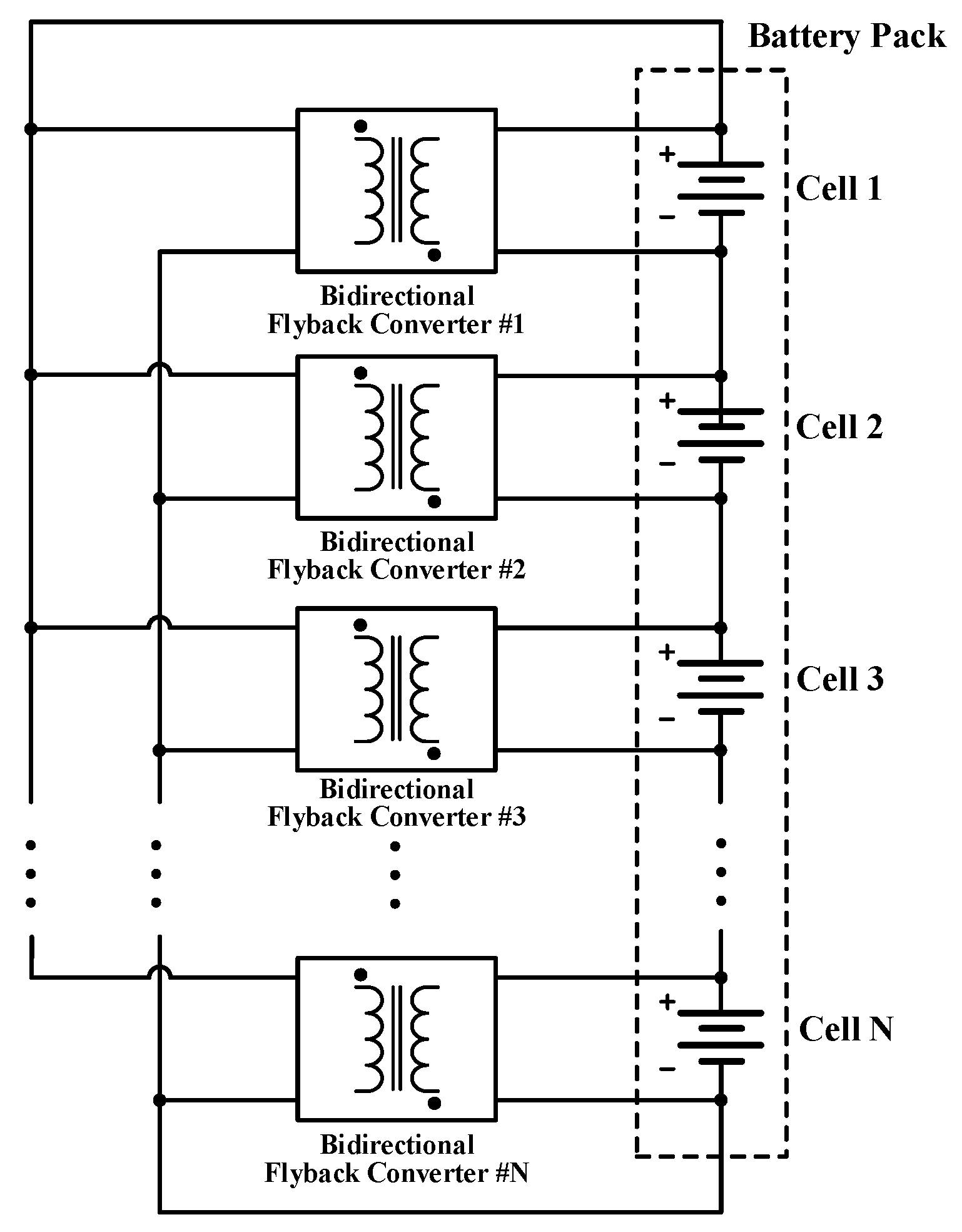
The proposed configuration is equipped with a symmetrical structure BFC for each cell, where all BFCs are connected in an input-parallel output-series (IPOS) configuration, which allows for efficient energy transfer in either direction between any two cells. Due to the modular design, it is easy to expand the system without redesigning the whole circuit.
(2)
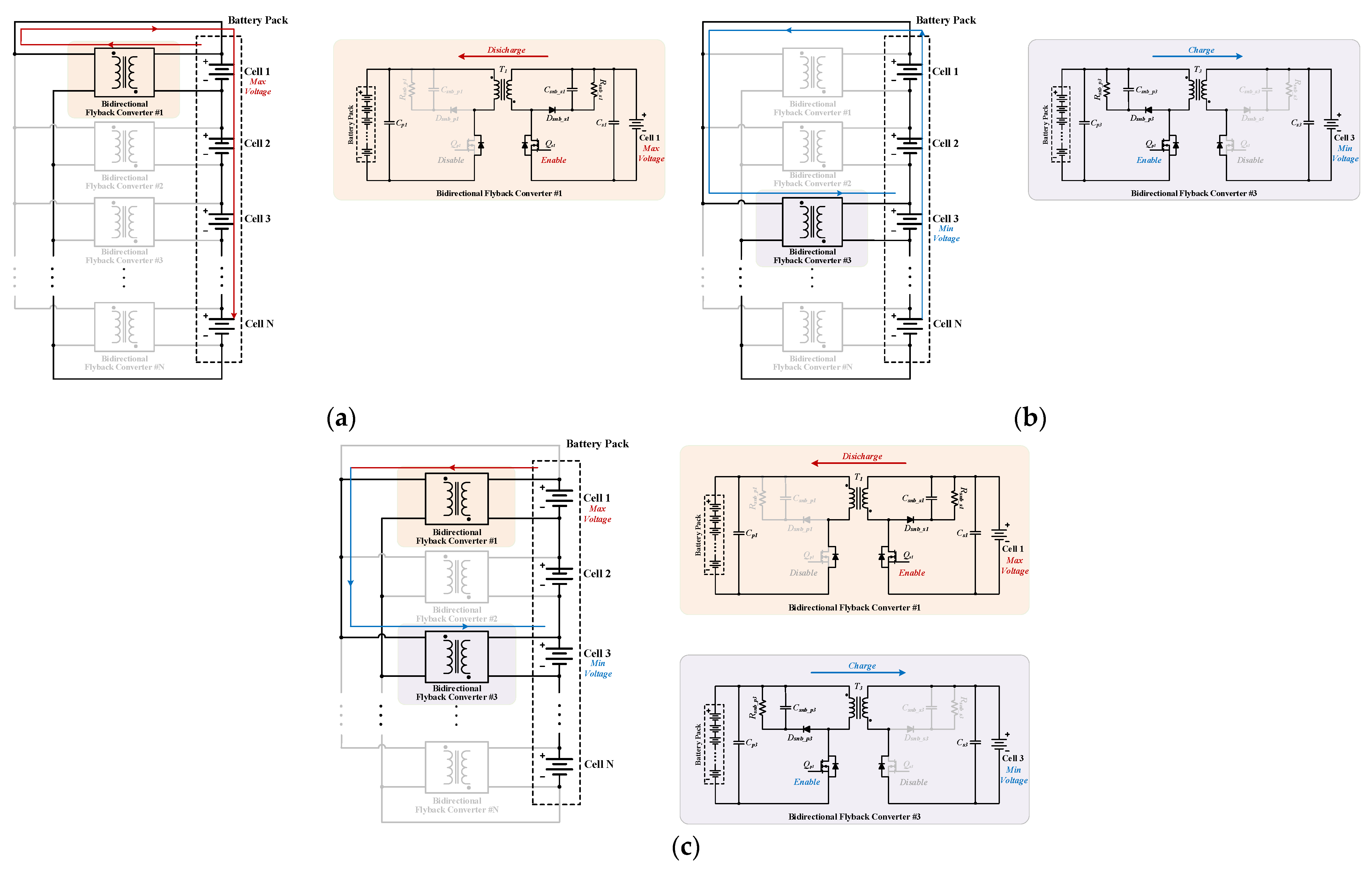
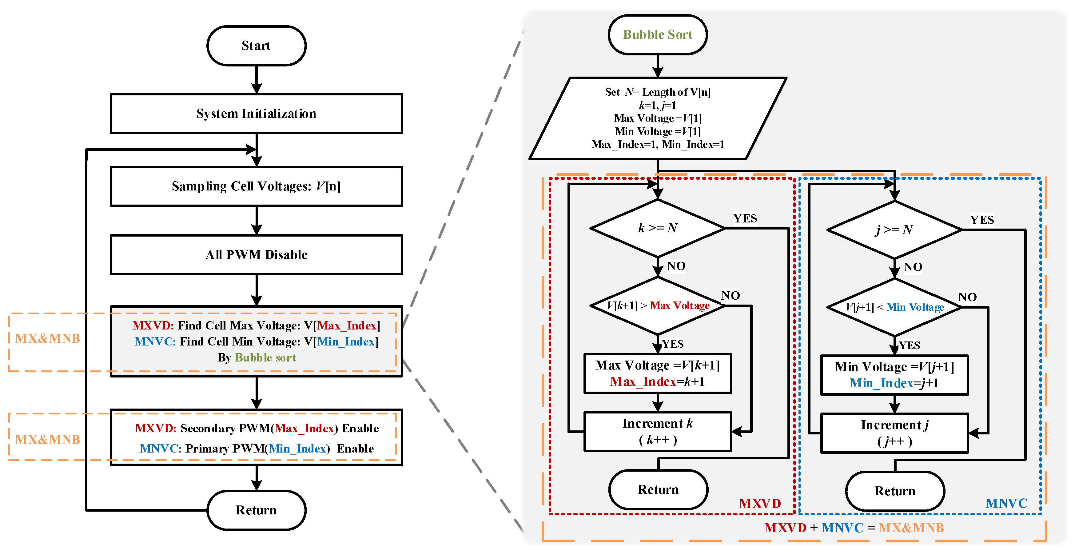
The charging/discharging mode of a particular cell could be controlled by adjusting the PWM signal on the primary or secondary side. The process of discharging the maximum voltage cell in the battery pack is called the maximum voltage discharge method (MXVD). Charging the minimum voltage cell with the minimum voltage is the minimum voltage charging method (MNVC). Combining the two methods to simultaneously control the discharging of the maximum voltage cell and charging of the minimum voltage cell is further proposed as the peer-to-peer energy transfer maximum and minimum voltage balancing method (MX&MNB). The algorithm and flowchart of the balancing strategies are described, which can be simply implemented in a low-cost microcontroller.
(3)
To validate the feasibility and balancing performance of the proposed configuration and methods, a cell balancing hardware prototype is designed and built. The experimental results show that all three proposed methods are effective in achieving cell balancing. Compared with MXVD and MNVC, the MX&MNB method enables energy transfer directly between the cells with the highest voltage difference, which effectively reduces the balancing time.
The remainder of this article is organized as follows. Section 2 describes the configuration of the cell balancing circuit based on BFC. Section 3 illustrates the principles and algorithms of the proposed three balancing strategies, and Section 4 discusses the proposed strategies through the simulation and experimental results. Finally, Section 5 concludes this paper.

2. The Cell Balancing Circuit Based on Bidirectional Flyback Converter

2.1. The Configuration of the Proposed Cell Balancing Circuit

Figure 1 shows the configuration of the proposed modular cell balancing circuit based on BFC. The battery pack consists of several cells connected in series, and these cells are required to achieve voltage equalization. Each cell is equipped with a symmetrically structured BFC, and the flyback converter is employed due to its galvanic isolation capability, simple design, and wide range of applications, which contributes to reducing the cost and complexity of the cell balancing circuit. All BFCs are connected in an IPOS configuration. Specifically, the primary side of all BFCs connects in parallel with the battery pack, while the secondary side is directly linked to each cell within the battery pack. The withstand voltage of the switching devices on the primary side should match the battery pack voltage, whereas switching devices with lower withstand voltages can be adopted on the secondary side. Since each cell is fitted with a BFC, it provides a higher degree of freedom for the bidirectional power flow and the control strategy.
The BFCs are usually employed in various low-power switching mode power supplies. The topology of a single BFC is shown in Figure 2, which consists of a transformer T with a turns ratio of n, two switching devices, and two RCD snubber circuits. The RCD snubber circuits are designed to absorb the energy stored in the leakage inductance, thus preventing the switching devices from damage due to high-voltage stresses. The BFC’s primary side voltage equals the battery pack voltage Vbat, and the secondary side voltage is the cell voltage Vcell. The difference with the conventional flyback converters is that the freewheel diode is replaced by a switching device, which provides the possibility of bidirectional operation. All BFCs have the same configuration and parameters with a symmetrical structure. This makes the design simple and efficient, facilitating modular application and expansion, so that it can be easily and flexibly adapted to different levels of battery systems.

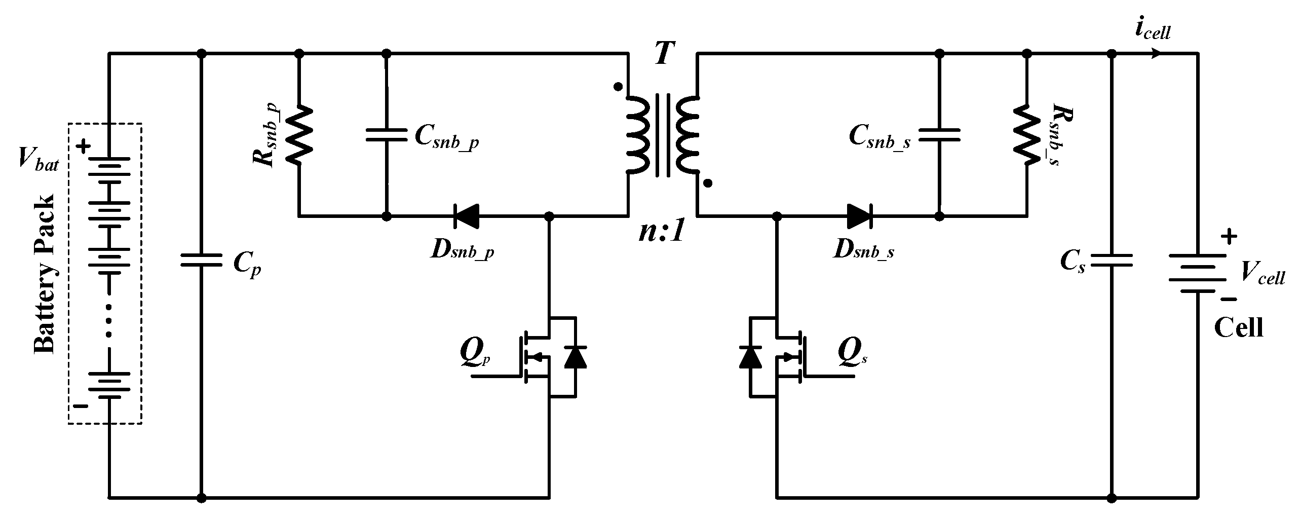
2.2. Operation Principle of Bidirectional Flyback Converter

There are two operation modes for flyback converters: current continuous mode (CCM) and current discontinuous mode (DCM). Comparatively, the DCM offers a better switching characteristic due to zero current switching of the rectifier diode, without reverse recovery, and the switching devices have lower turn-on voltages, which results in higher efficiency of the flyback in the DCM. In addition, the transformer size is smaller in DCM because the transformer stores less energy at the same power level.
When the cell is charged, energy is transferred from the primary side to the secondary side of the BFC. The primary side switching device Qp operates in PWM, and the secondary side switching device Qs is always turned OFF. For the DCM, a switching period Ts can be roughly divided into four operating stages, and Figure 3a–d illustrate the circuit states of each stage. Meanwhile, Figure 3e shows the operating waveforms of the BFC operating in DCM. Qp and vDS are the driving signal and drain-source voltage of the primary side switching device, respectively. Ton is the conduction period of Qp (Ton = don_fTs), Toff represents the flux reset period (Toff = dp_fTs), and Tres is the current discontinuous period.
Stage 1 (t0t1): As shown in Figure 3a, at t0, Qp is turned ON, while the secondary side Qs is turned OFF. The primary side voltage of T is equal to Vbat, so the primary side inductor current ip increases linearly, and thus the transformer stores energy. Csnb_p is discharged slowly by Rsnb_p. At t1, Qp is turned OFF, and Stage 1 is finished.
Stage 2 (t1t2): As shown in Figure 3b, at t1, Qp is turned OFF, and its parasitic capacitance is charged, so vDS rises rapidly. Until the primary side inductor voltage is clamped, the body diode of Qs starts to turn ON, and T transfers energy to the secondary side. At the same time, Dsnb_p is ON, and the energy stored in the leakage inductance is transferred to Csnb_p. ip is in the same direction as in Stage 1, but the amplitude decreases rapidly.
Stage 3 (t2t3): As shown in Figure 3c, at t2, ip decreases to 0, and Dsnb_p is turned OFF. vds remains at Vbat + nVcell, and T continues to deliver energy to the secondary side. Since the voltage on the secondary side of T is clamped by Vcell, the diode current iD on the secondary side will decrease linearly.
Stage 4 (t3t4): As shown in Figure 3d, at t3, iD drops to 0, the voltage clamping disappears, and the body diode of Qs is turned OFF. At t4, Qp is turned ON again, and the converter enters into the next switching period, repeating the same operating state as described above.
When the cell is discharged, the energy is transferred from the secondary side to the primary side, and the BFC operates in reverse mode. At this time, due to the completely symmetrical structure, the operating principle and waveform of the BFC are similar to the forward mode shown in Figure 3. The difference is that the secondary side Qs is in PWM, the primary side Qp is always OFF, and the body diode of Qp acts as a freewheel diode. The description of the reverse mode operation state will not be repeated here.
To ensure that the BFC operates in DCM, the duty cycle don_f of Qp in forward mode should satisfy the following conditions.
d o n _ f < n V c e l l n V c e l l + V b a t
The duty cycle don_r of Qs in reverse mode shall meet the following conditions.
d o n _ r < V b a t / n V b a t / n + V c e l l
As shown in Figure 3, in the forward mode of DCM, the average cell charging current icell can be expressed as
i c e l l = 1 2 Δ i D d p _ f
The ΔiD in Toff is given by the following equation.
Δ i D = n V b a t d f T s L m p
where Lmp is the magnetization inductance of the transformer’s primary side. According to the voltage relationship on the output side, dp_f can be represented as
d p _ f = V b a t d o n _ f n V c e l l
Neglecting the losses, the cell charging power Pch through a single BFC at a steady state can be calculated as follows
P c h = V b a t 2 d o n _ f 2 2 L m p T s 2
According to the above equation, when the switching frequency and duty cycle of Qp are constant, Pch is also constant. Similarly, the cell discharging power Pdis through a single BFC in the reverse mode can be formulated as follows
P d i s = V c e l l 2 d o n _ r 2 2 L m p / n 2 T s 2

3. The Proposed Cell Balancing Strategy

3.1. The Working Principle of the Balancing Strategy

According to the operating principle of a BFC, when the switching device on the primary side of a BFC is enabled, and the switching device on the secondary side is disabled, and the energy is transferred from the primary side to the secondary side to charge the corresponding cell. Vice versa, when the primary side is disabled, and the secondary side is enabled, energy is delivered from the secondary side to the primary side to discharge the corresponding cell. The control and switching of the charging/discharging mode for a specific cell can be realized by adjusting the PWM signal on the primary or secondary side.
This structure allows for the free transmission of energy between any two cells or one cell and the battery pack, thus providing different implementation strategies and more control possibilities for C2C and C2P. Three cell balancing strategies are proposed: (1) maximum voltage discharge (MXVD), (2) minimum voltage charge (MNVC), and (3) maximum and minimum voltage balancing (MX&MNB), and the strategies are explained in the following text.
Assuming the same external conditions for all three strategies, the voltage of Cell1 in the battery pack is maximum, and the voltage of Cell3 is minimum.
(1)
MXVD
As shown in Figure 4a, BFC#1 corresponds to Cell1, whose primary side Qp1 is disabled, while the secondary side Qs1 is enabled, and BFC#1 operates in the reverse mode. At this time, Cell1 is discharged through BFC#1. Only Qs1 is enabled, while all other devices are disabled. Therefore, only BFC#1 is involved in energy transfer, where Cell1 is discharged, and energy is transferred from the secondary side to the primary side, thus charging the whole battery pack. The power flow path is shown as the red line in Figure 4a.
(2)
MNVC
As shown in Figure 4b, BFC#3 corresponds to Cell3, whose secondary side Qs3 is disabled, while the primary side Qp3 is enabled, and BFC#3 operates in the forward mode. At this time, Cell3 is charged through BFC#3. In this mode, only Qp3 is enabled, while all other devices are disabled. Therefore, the whole battery pack is discharged through BFC#3, and the energy is transferred from the primary side to the secondary side to charge Cell3. The power flow path is shown as the blue line in Figure 4b.
(3)
MX&MNB
As shown in Figure 4c, Qp1 is disabled, and Qs1 is enabled in BFC#1; meanwhile, Qs3 is disabled, and Qp3 is enabled in BFC#3. Then, BFC#1 operates in the reverse mode, and BFC#3 operates in the forward mode. At this time, Cell1 is discharged through BFC#1, and Cell3 is charged through BFC#3. Qs1 and Qp3 are enabled, and all other devices are disabled. Therefore, only BFC#1 and BFC#3 are involved in energy transfer. The energy discharged from Cell1 to the primary side of BFC#1 will charge Cell3 through BFC#3. The energy is transferred between the two cells with the largest voltage difference, and the power flow path is shown by the arrows in Figure 4c.
Figure 4. The proposed three cell balancing strategies based on bidirectional flyback converter. (a) Maximum voltage discharge. (b) Minimum voltage charging. (c) Maximum and minimum voltage balancing.
Batteries 11 00168 g004

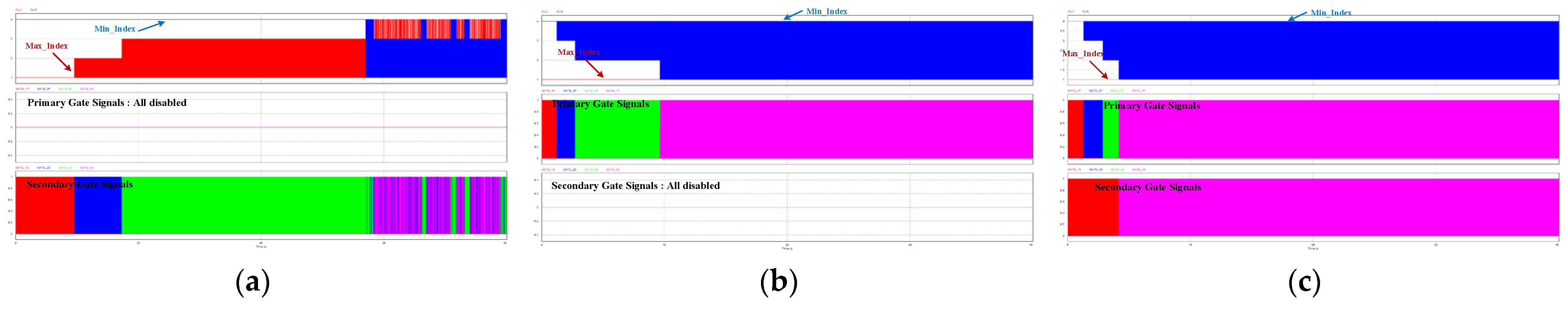
3.2. Cell Balancing Algorithm

Figure 5 shows the flowchart of the proposed algorithm for the BFC-based cell balancing strategy. First, after system initialization, the voltage of each cell is sampled, and the PWM of all switching devices is disabled. Then, the cell with the maximum and minimum voltages is located with the bubble sort algorithm, respectively. Bubble sort is a simple and efficient method, taking the process of finding the cell with the maximum voltage as an example. Each round of sorting starts with the voltage of Cell1, which is compared with the voltage of Cell2, and the larger of the two is set as the maximum. The maximum value is then compared to the voltage of Cell3, and the larger one is assigned as the new maximum. The process is repeated until all the cell voltages are traversed, and the cell with the maximum voltage can be identified. The process of finding the cell with the minimum voltage is similar.
Next, according to the cell numbering with the maximum and minimum voltage, the three cell balancing strategies are implemented by controlling the corresponding switching signals on the primary or secondary side. For MXVD, the secondary side switching device of the BFC corresponding to the cell with the maximum voltage is enabled to control the discharge of that cell. For MNVC, the switching device on the primary side of the BFC corresponding to the cell with the minimum voltage is enabled to control the charging of that cell. For MX&MNB, it is essentially a combination of MXVD and MNVC. The switching device on the secondary side of the BFC corresponding to the maximum voltage cell and the switching device on the primary side of the BFC corresponding to the minimum voltage cell are turned ON, which allows for the maximum voltage cell to charge the minimum voltage cell directly without passing through the entire battery pack.
Theoretically, the balancing speed and efficiency of MX&MNB will be better than the other two methods, but the complexity of their control strategies is similar. MX&MNB allows the two cells with the largest voltage difference to be balanced simultaneously, even if they are not adjacent to each other, regardless of their position in the battery pack. Therefore, MX&MNB can achieve cell voltage balancing with a highly flexible and simple control strategy. In addition, the proposed strategy offers the possibility of extension. For battery systems with low to medium voltage levels, the number of series-connected cells is usually small. The computational burden of bubble sorting is negligible, especially considering the relatively slow voltage dynamics of the cells, which can be simply implemented in a low-cost microcontroller for verification and debugging.

4. Simulation and Experimental Verification
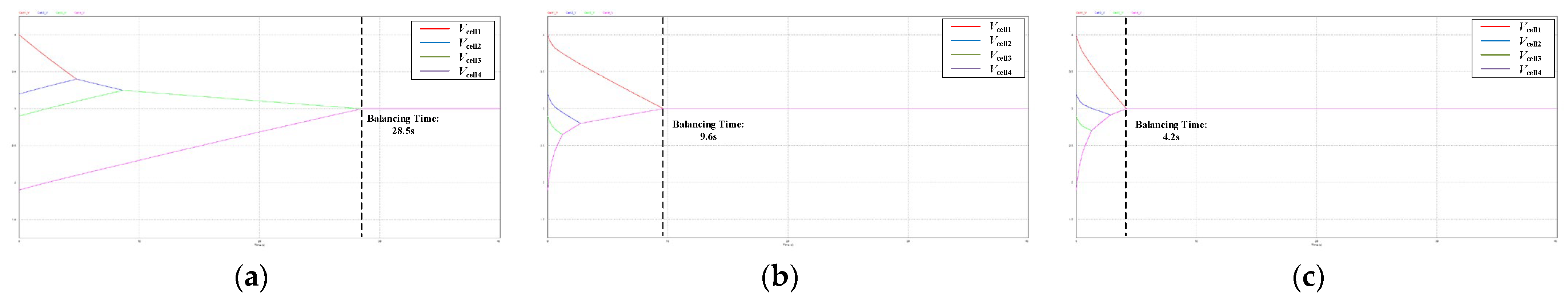
4.1. Simulation

The proposed cell balancing circuit based on BFC and three balancing strategies are simulated with PSIM 9.1.1 software. The specific parameter specifications in the simulation are shown in Table 1. The battery pack consists of four cells connected in series, and the initial voltages of the four cells are 4.0 V, 3.2 V, 2.9 V, and 1.9 V. Figure 6a–c show the cell balancing waveforms under the same conditions employing MXVD, MNVC, and MX&MNB, respectively. Table 2 compares the required balancing time for the three proposed strategies in the simulation, and it can be seen that all three strategies can effectively achieve cell voltage balancing, but MX&MNB offers the fastest balancing speed.
Figure 7a–c show the driving waveforms under the three strategies, respectively. Among them, the top screen shows the maximum voltage cell number Max_Index and the minimum voltage cell number Min_Index, the middle screen shows the four gate signals on the primary side, and the bottom screen shows the four gate signals on the secondary side. MXVD is taken as an example for illustration. Under the initial condition, Vcell1 is the maximum, so Max_Index = 1. At this time, Qs1 on the secondary side of BFC#1 operates in PWM (as the red waveform shown in the bottom screen), while the other PWMs are disabled, and Cell1 is discharged to the battery pack through BFC#1. The Vcell1 gradually decreases, and the voltage of the other three cells gradually increases, which can be verified from Figure 6a. When Vcell1 drops to less than Vcell2, Max_Inde = 2. Qs2 on the secondary side of BFC#2 operates in PWM (as the blue waveform shown in the bottom screen), while the other PWMs are disabled, and Cell2 discharges to the battery pack through BFC#2. When Vcell2 drops to less than Vcell1, Max_Index = 1, so Cell1 will start discharging again. Therefore, Max_Index keeps switching between 1 and 2 (as the red waveform shown in the top screen), and Cell1 and Cell2 will take turns to discharge as the highest-voltage cell. Macroscopically, when there are multiple cells with the maximum voltage, these cells will be discharged alternately, with the voltage decreasing at approximately the same rate. Until the voltage of all the cells reaches the same value, the balancing process is over.
In MNVC, the alternating charging process of the minimum voltage cell is similar to the alternating discharging process described above, and so it will not be repeated here. MX&MNB is a combination of MXVD and MNVC, and the maximum voltage cell will be alternately discharged; meanwhile, the minimum voltage cell will be alternately charged. However, there is only one switching device on the primary side and one on the secondary side to turn ON during the same moment; in other words, there are always only two BFCs involved in the energy transfer. Because the charging/discharging of a single cell no longer passes entirely through the pack, MX&MNB balancing is faster. The proposed balancing method is based on a BFC architecture, which enables non-adjacent C2C energy transfer without routing all energy through a centralized storage element or bus. This structure inherently reduces the number of conversion stages and direct energy transfer, which enables minimizing power conversion losses.

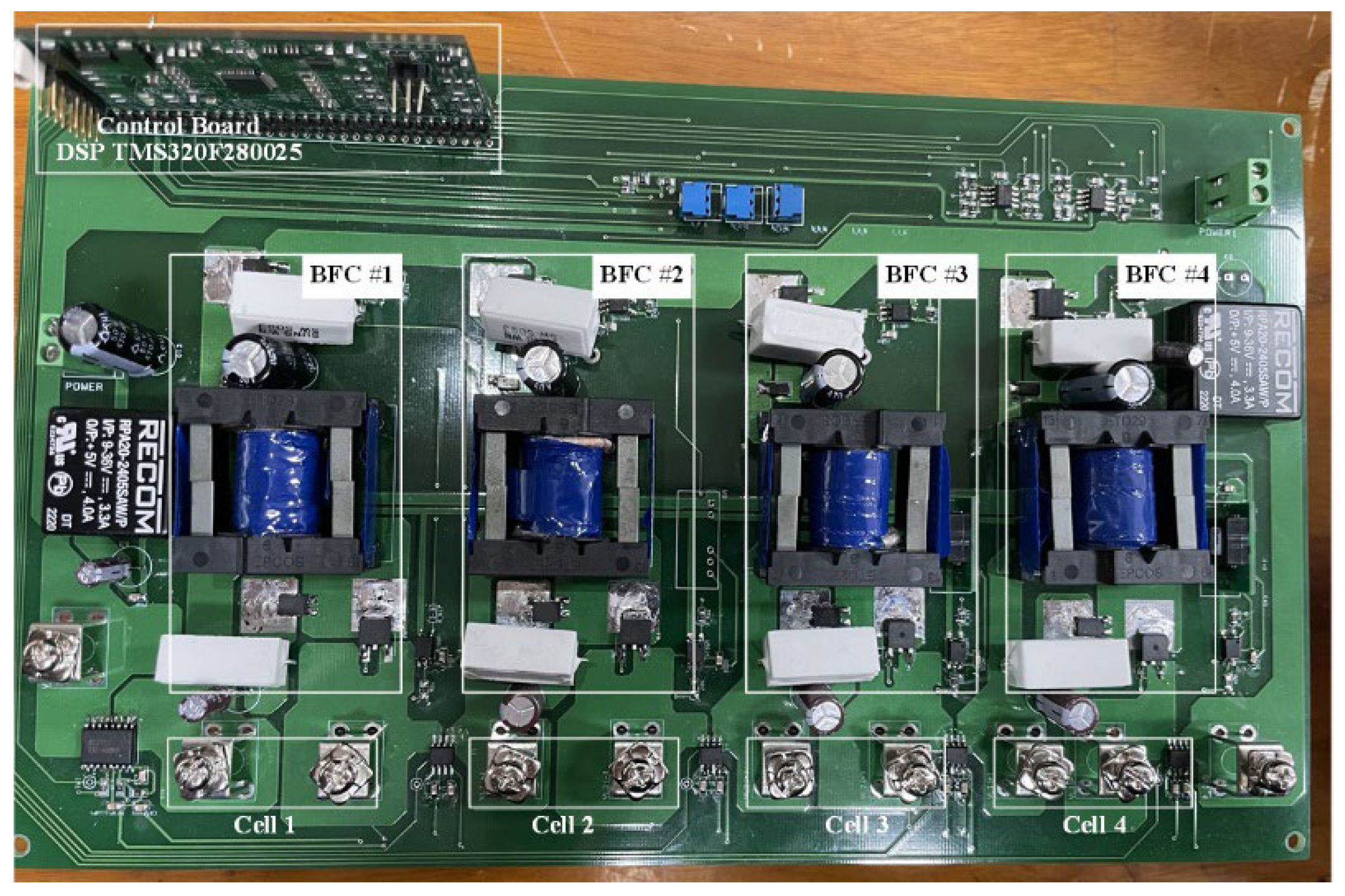
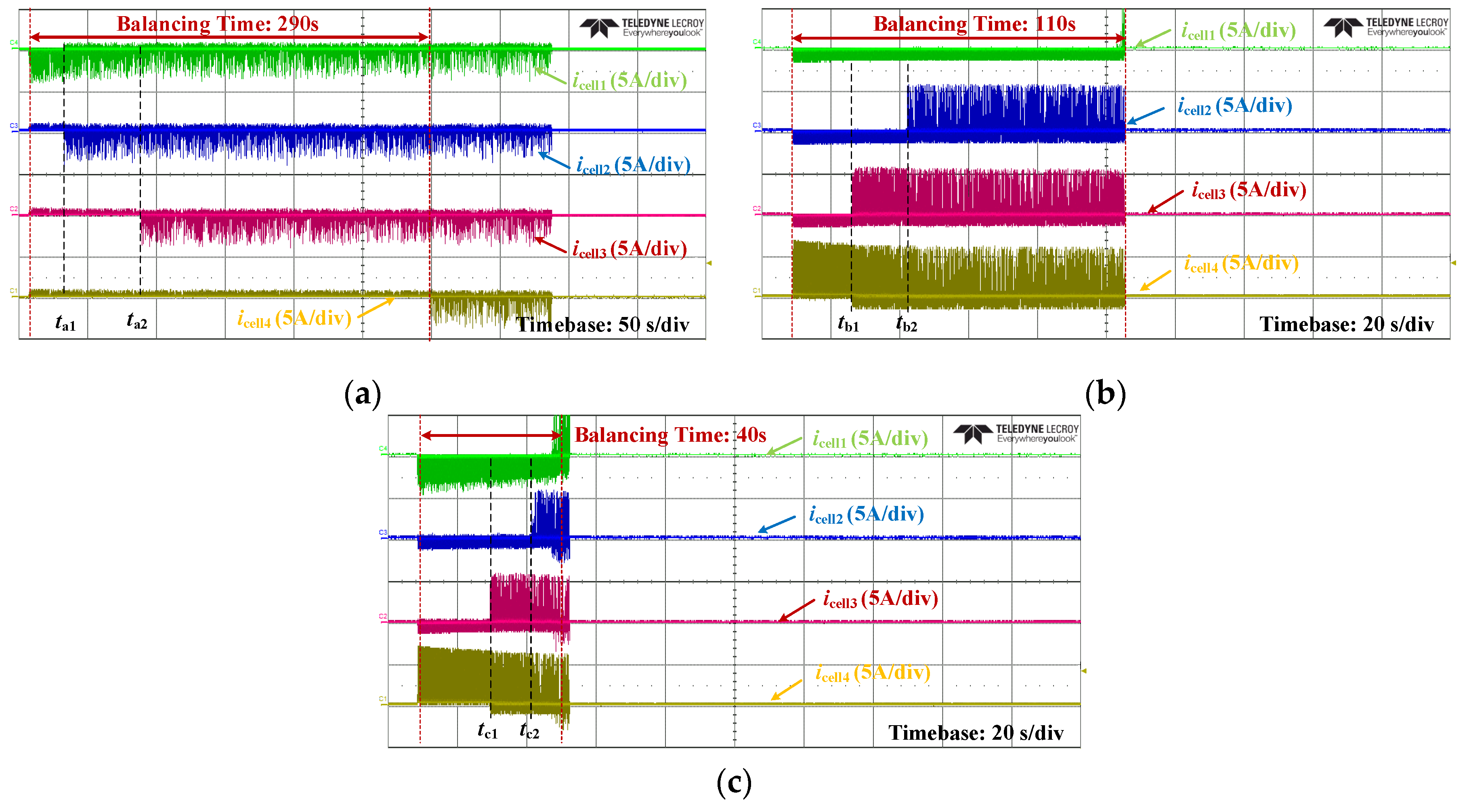
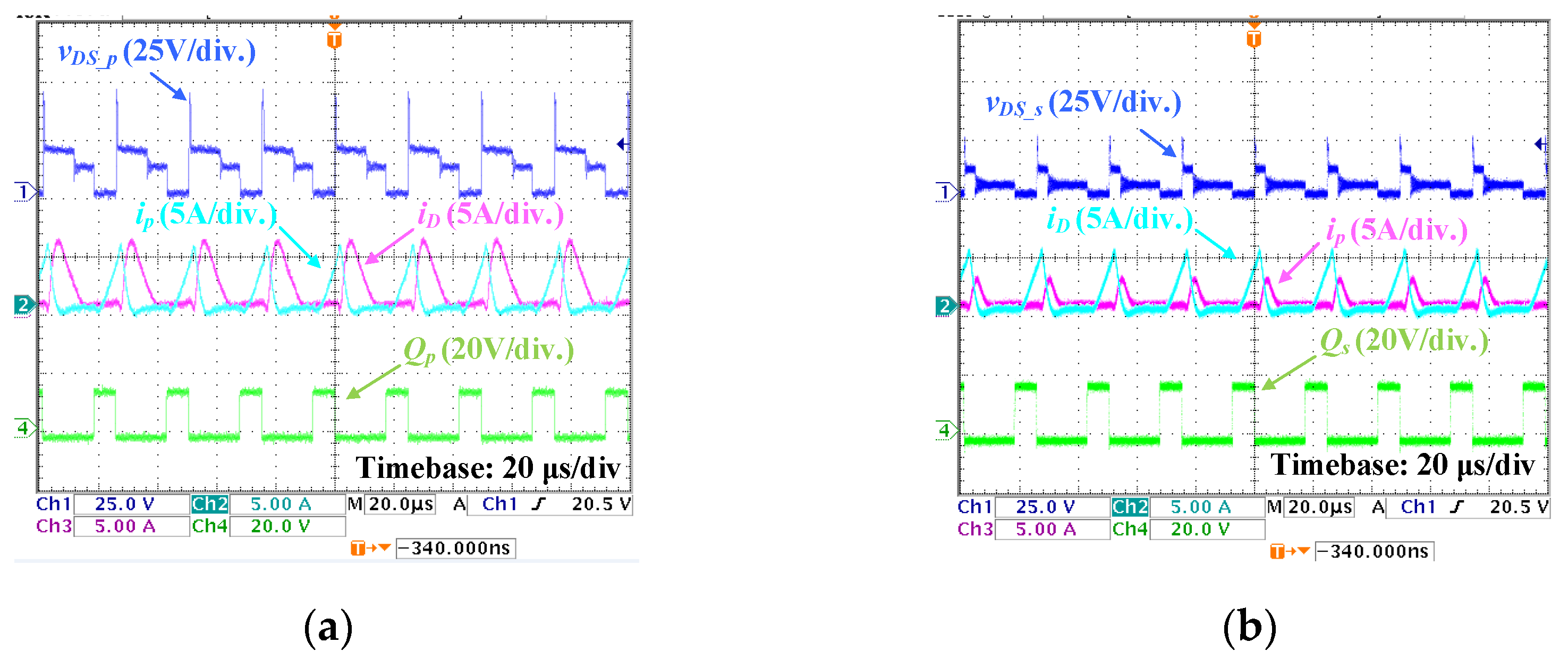
4.2. Experimental Verification

To verify the validity of the proposed BFC-based modular cell balancing circuit and methods, a prototype was designed and built with the configuration shown in Figure 8. The specific parameters of the prototype are the same as the simulation, as shown in Table 1. The main controller is a DSP TMS320F280025. The main objective of the prototype is to validate the feasibility and balancing performance of the proposed circuit and strategy. Considering factors such as fast charge/discharge, convenience, safety, and flexibility, supercapacitors are adopted instead of lithium-ion batteries in the experiments to facilitate the demonstration of the dynamic behavior of voltage balancing in an oscilloscope. The three methods are compared under the same conditions and parameters.
Figure 9a–c show the experimental waveforms of the three balancing strategies, respectively, in which the trends of the cell voltages are similar to the simulation waveforms. Table 3 compares the balancing time of the three proposed strategies in the experiments, and it can be seen that, identical to the simulation results, MX&MNB offers the fastest balancing speed.
Figure 10a–c show the cell current waveforms under the three balancing strategies, respectively. For MXVD, Vcell1 is the maximum voltage under the initial condition, Cell1 discharges first, and the other three cells are charged. As can be seen, before ta1, the green waveform amplitude corresponding to Cell1 is negative, while the amplitudes of the other three waveforms are positive. At ta1, Vcell1 drops to be equal to Vcell2, so Cell1 and Cell2 charge the other three cells alternately as the maximum voltage cell. The blue waveform corresponding to Cell2 also begins to show negative amplitude. Between ta1 and ta2, both the green and blue waveforms have parts with positive amplitudes, indicating that Cell1 and Cell2 are discharging alternately. At ta2, Vcell1 and Vcell2 are equal to Vcell3, at which point Cell1, Cell2, and Cell3 take turns charging the other cells. Only the yellow waveform corresponding to Cell4 has positive amplitude values, indicating that only Cell4, which has the lowest voltage, remains in the charging state. The current waveforms can be correlated with the voltage changes shown in Figure 9a. For MNVC, Cell4, which has the minimum initial voltage, is charged first, and the other three cells are discharged, and the process is similar to MXVD. For MX&MNB, Cell1 discharges while Cell4 charges, and most of the charging energy of Cell4 comes from Cell1. Before tc1, the green waveform corresponding to Cell1 has a negative amplitude and is always discharging, while the yellow waveform corresponding to Cell4 has a positive amplitude and is always charging. At tc1, Cell3 and Cell4 alternate as the minimum voltage cell to charge. At tc2, Cell2, Cell3, and Cell4 are alternately charged, and Cell1 is always discharged through BFC#1.
It can be seen that the charging power of a single cell through the BFC is larger than the discharging power with a fixed duty cycle, and thus the balancing speed of the MNVC is faster than that of the MXVD when only one BFC is involved in the energy transfer. In MX&MNB, the discharging power of the cell with the maximum voltage is greater than that of MNVC, so the balancing speed of MX&MNB is faster than that of MNVC.
The waveforms of BFC in forward and reverse operating modes are shown in Figure 11a,b, respectively. Similarly to the theoretically analyzed waveforms, the BFC operates stably in DCM during both charging and discharging. To fully evaluate the performance of the three balancing strategies, the waveforms under different duty cycle conditions are shown in Figure 12. Specifically, the duty cycle is set to 0.2 to compare with the case of a duty cycle of 0.1, as shown in Figure 9. It can be seen that the balancing speed increases when the duty cycle increases. The MX&MNB still offers the fastest balancing speed among the three methods.
Table 4 compares the proposed method with previous works. Compared to previous works, the proposed method avoids the switching matrix and adopts a simpler and more generalized flyback topology, resulting in a smaller number of switching devices and inductors. Although it is necessary to equip each cell with a transformer, due to the modular feature of the BFC, the transformers are of identical parameters, which contributes to the design and cost reduction. Owing to the modular design, the proposed cell balancing circuit can be extended more flexibly. At the same time, the proposed circuit allows for individual control of the bidirectional power flow for each cell, which can provide more control possibilities. Therefore, overall, the proposed BFC-based cell balancing circuit offers advantages in terms of cost, complexity, and expandability.
Modular designs inevitably involve tradeoffs between hardware redundancy and extensibility, which increases size and cost. However, it improves maintainability and fault tolerance, and the cost could be compensated by improved safety and reliability. The number of cells that can be supported in a voltage balancing system is limited by the number of PWM channels in the employed DSP. While prototypes are built with discrete components to facilitate testing and increase flexibility, there is still significant potential for integration and miniaturization using custom PCBs or specialized integrated circuits.

5. Conclusions

This paper presents a modular cell balancing circuit based on a BFC. Each cell is equipped with a symmetrically structured BFC, forming a flexible IPOS configuration. The primary side of all BFCs is connected in parallel with the battery pack, and the secondary side is connected to individual cells. This architecture enables direct and efficient energy transfer between individual cells and the battery pack, supporting high flexibility with minimal additional complexity. The control of the charging/discharging mode of a specific cell can be realized by adjusting the PWM signals on the primary or secondary side. Based on this configuration, three balancing strategies are proposed: MXVD, MNVC, and MX&MNB. Particularly, the MX&MNB method allows for direct energy flow between the two cells with the largest voltage difference, effectively improving the balancing speed without passing energy through the battery pack, which is essentially a combination of MXVD and MNVC. The simulations and experimental results confirm the feasibility and effectiveness of the proposed methods. Experimental verification shows that MX&MNB significantly improves balancing speed compared to MXVD and MNVC. Specifically, the balancing time of MX&MNB is 7.25 times and 2.75 times faster than that of MXVD and MNVC, respectively. This quantitative result indicates that MX&MNB significantly reduces losses by directly transferring energy between cells with the largest voltage differences, thereby achieving more efficient balancing. Overall, the proposed BFC-based cell balancing circuit offers more advantages in terms of efficiency, complexity, and scalability due to the modular design.

Author Contributions

Conceptualization, G.Z. and S.-J.P.; data curation, S.-C.C.; funding acquisition, G.Z.; investigation, J.-H.K. and S.-C.C.; project administration, G.Z.; software, Y.W.; supervision, S.-J.P.; validation, J.-H.K. and S.-C.C.; visualization, S.-C.C.; writing—original draft, Y.W. and J.-H.K.; writing—review and editing, Y.W. All authors have read and agreed to the published version of the manuscript.

Funding

This research was funded in part by the Shandong Province “Double-Hundred Talent Plan”, under Grant WST2024010; in part by the Key technology research project in Qingdao, under Grant 25-1-1-gjgg-4-gx; and in part by the Gwangju Chonnam Local Energy Cluster Human Resources Development of Korea Institute of Energy Technology Evaluation and Planning under grant Korea government Ministry of Knowledge Economy, grant number 20214000000560.

Data Availability Statement

The original contributions presented in the study are included in the article, further inquiries can be directed to the corresponding authors.

Acknowledgments

The authors thank the Industrial Electronics Application Laboratory of Chonnam National University for providing experimental equipment. This article is a revised and expanded version of a paper entitled “A Cell-to-cell Voltage Balancing Strategy with Bidirectional Flyback Converter”, which was presented at the 2024 IEEE 10th International Power Electronics and Motion Control Conference (IPEMC2024-ECCE Asia), Chengdu, China.

Conflicts of Interest

The authors declare no conflicts of interest.

Abbreviations

The following abbreviations are used in this manuscript:
BFCBidirectional flyback converter
MXVDMaximum voltage discharge
MNVCMinimum voltage charge
MX&MNBMaximum and minimum voltage balancing
IPOSInput-parallel output-series
C2CCell-to-cell
C2PCell-to-pack
CCMCurrent continuous mode
DCMCurrent discontinuous mode

References

  1. Lin, T.; Chen, Z.; Zheng, C.; Huang, D.; Zhou, S. Fault Diagnosis of Lithium-Ion Battery Pack Based on Hybrid System and Dual Extended Kalman Filter Algorithm. IEEE Trans. Transp. Electrif. 2021, 7, 26–36. [Google Scholar] [CrossRef]
  2. Lim, C.-S.; Lee, K.-J.; Ku, N.-J.; Hyun, D.-S.; Kim, R.-Y. A Modularized Equalization Method Based on Magnetizing Energy for a Series-Connected Lithium-Ion Battery String. IEEE Trans. Power Electron. 2014, 29, 1791–1799. [Google Scholar] [CrossRef]
  3. Chen, M.; Rincon-Mora, G.A. Accurate electrical battery model capable of predicting runtime and I-V performance. IEEE Trans. Energy Convers. 2006, 21, 504–511. [Google Scholar] [CrossRef]
  4. Kwon, J.-H.; Choi, S.-C.; Zhou, G.; Park, S.-M.; Park, S.-J.; Wang, Y. A Cell-to-cell Voltage Balancing Strategy with Bidirectional Flyback Converter. In Proceedings of the 2024 IEEE 10th International Power Electronics and Motion Control Conference (IPEMC2024-ECCE Asia), Chengdu, China, 17–20 May 2024; pp. 4088–4093. [Google Scholar] [CrossRef]
  5. El Ghossein, N.; Sari, A.; Venet, P. Effects of the Hybrid Composition of Commercial Lithium-Ion Capacitors on Their Floating Aging. IEEE Trans. Power Electron. 2019, 34, 2292–2299. [Google Scholar] [CrossRef]
  6. Milas, N.T.; Tatakis, E.C. Fast Battery Cell Voltage Equalizer Based on the Bidirectional Flyback Converter. IEEE Trans. Transp. Electrif. 2023, 9, 4922–4940. [Google Scholar] [CrossRef]
  7. Zhang, Z.; Gui, H.; Gu, D.-J.; Yang, Y.; Ren, X. A Hierarchical Active Balancing Architecture for Lithium-Ion Batteries. IEEE Trans. Power Electron. 2017, 32, 2757–2768. [Google Scholar] [CrossRef]
  8. Wang, Y.; Kim, S.-Y.; Chen, Y.; Zhang, H.; Park, S.-J. An SMPS-Based Lithium-Ion Battery Test System for Internal Resistance Measurement. IEEE Trans. Transp. Electrif. 2023, 9, 934–944. [Google Scholar] [CrossRef]
  9. Shang, Y.; Zhu, C.; Fu, Y.; Mi, C.C. An Integrated Heater Equalizer for Lithium-Ion Batteries of Electric Vehicles. IEEE Trans. Ind. Electron. 2019, 66, 4398–4405. [Google Scholar] [CrossRef]
  10. Naguib, M.; Kollmeyer, P.; Emadi, A. Lithium-Ion Battery Pack Robust State of Charge Estimation, Cell Inconsistency, and Balancing: Review. IEEE Access 2021, 9, 50570–50582. [Google Scholar] [CrossRef]
  11. Izadi, Y.; Beiranvand, R. A Comprehensive Review of Battery and Supercapacitor Cells Voltage-Equalizer Circuits. IEEE Trans. Power Electron. 2023, 38, 15671–15692. [Google Scholar] [CrossRef]
  12. Raeber, M.; Heinzelmann, A.; Abdeslam, D.O. Analysis of an Active Charge Balancing Method Based on a Single Nonisolated DC/DC Converter. IEEE Trans. Ind. Electron. 2021, 68, 2257–2265. [Google Scholar] [CrossRef]
  13. Qi, X.; Wang, Y.; Fang, M.; Liu, W. A Reduced-Component-Count Centralized Equalization System for Series-Connected Battery Packs Based on a Novel Integrated Cascade Topology. IEEE Trans. Ind. Appl. 2021, 57, 6105–6116. [Google Scholar] [CrossRef]
  14. Qi, X.; Wang, Y.; Wang, Y.; Chen, Z. Optimization of Centralized Equalization Systems Based on an Integrated Cascade Bidirectional DC–DC Converter. IEEE Trans. Ind. Electron. 2022, 69, 249–259. [Google Scholar] [CrossRef]
  15. Xiong, H.; Song, D.; Shi, F.; Wei, Y.; Jinzhen, L. Novel voltage equalisation circuit of the lithium battery pack based on bidirectional flyback converter. IET Power Electron. 2020, 13, 2194–2200. [Google Scholar] [CrossRef]
  16. Zhou, G.; Zhang, X.; Gao, K.; Tian, Q.; Xu, S. Two-Mode Active Balancing Circuit Based on Switched-Capacitor and Three-Resonant-State LC Units for Series-Connected Cell Strings. IEEE Trans. Ind. Electron. 2022, 69, 4845–4858. [Google Scholar] [CrossRef]
  17. Nazi, H.; Babaei, E. A Modularized Bidirectional Charge Equalizer for Series-Connected Cell Strings. IEEE Trans. Ind. Electron. 2021, 68, 6739–6749. [Google Scholar] [CrossRef]
  18. Qi, X.; Wang, Y.; Fang, M.; Wang, Y.; Chen, Z. Multiport DC–DC Converter with Integrated Cascaded Structure for Optimizing Centralized Battery Equalization System. IEEE Trans. Power Electron. 2022, 37, 15111–15126. [Google Scholar] [CrossRef]
  19. Avila, A.; Garcia-Bediaga, A.; Alzuguren, I.; Vasić, M.; Rujas, A. A Modular Multifunction Power Converter Based on a Multiwinding Flyback Transformer for EV Application. IEEE Trans. Transp. Electrif. 2022, 8, 168–179. [Google Scholar] [CrossRef]
  20. Lee, J.-H.; Park, S.-J.; Lim, S.-K. Improvement of Multilevel DC/DC Converter for E-Mobility Charging Station. Electronics 2020, 9, 2037. [Google Scholar] [CrossRef]
  21. Jaguemont, J.; Boulon, L.; Dubé, Y. A comprehensive review of lithium-ion batteries used in hybrid and electric vehicles at cold temperatures. Appl. Energy 2016, 164, 99–114. [Google Scholar] [CrossRef]
  22. Ding, X.; Zhang, D.; Cheng, J.; Wang, B.; Chai, Y.; Zhao, Z.; Xiong, R.; Luk, P.C.K. A Novel Active Equalization Topology for Series-Connected Lithium-ion Battery Packs. IEEE Trans. Ind. Appl. 2020, 56, 6892–6903. [Google Scholar] [CrossRef]
  23. Tashakor, N.; Farjah, E.; Ghanbari, T. A Bidirectional Battery Charger with Modular Integrated Charge Equalization Circuit. IEEE Trans. Power Electron. 2017, 32, 2133–2145. [Google Scholar] [CrossRef]
  24. Kim, M.-Y.; Kim, J.-H.; Moon, G.-W. Center-Cell Concentration Structure of a Cell-to-Cell Balancing Circuit with a Reduced Number of Switches. IEEE Trans. Power Electron. 2014, 29, 5285–5297. [Google Scholar] [CrossRef]
  25. Shang, Y.; Zhang, C.; Cui, N.; Guerrero, J.M. A Cell-to-Cell Battery Equalizer with Zero-Current Switching and Zero-Voltage Gap Based on Quasi-Resonant LC Converter and Boost Converter. IEEE Trans. Power Electron. 2015, 30, 3731–3747. [Google Scholar] [CrossRef]
  26. Lee, K.-M.; Lee, S.-W.; Choi, Y.-G.; Kang, B. Active Balancing of Li-Ion Battery Cells Using Transformer as Energy Carrier. IEEE Trans. Ind. Electron. 2017, 64, 1251–1257. [Google Scholar] [CrossRef]
  27. Wang, Y.; Kim, S.-Y.; Zhang, H.; Chen, Y.; Park, S.-J. Design and analysis of an input-series quasi-resonant flyback high-voltage SMPS based on an integrated transformer. IET Power Electron. 2022, 15, 1058–1074. [Google Scholar] [CrossRef]
  28. Mahafzah, K.A.; Obeidat, M.A.; Al-Shetwi, A.Q.; Ustun, T.S. A Novel Synchronized Multiple Output DC-DC Converter Based on Hybrid Flyback-Cuk Topologies. Batteries 2022, 8, 93. [Google Scholar] [CrossRef]
  29. Hannan, M.A.; Hoque, M.M.; Peng, S.E.; Uddin, M.N. Lithium-Ion Battery Charge Equalization Algorithm for Electric Vehicle Applications. IEEE Trans. Ind. Appl. 2017, 53, 2541–2549. [Google Scholar] [CrossRef]
  30. Chen, Y.; Liu, X.; Cui, Y.; Zou, J.; Yang, S. A MultiWinding Transformer Cell-to-Cell Active Equalization Method for Lithium-Ion Batteries with Reduced Number of Driving Circuits. IEEE Trans. Power Electron. 2016, 31, 4916–4929. [Google Scholar]
  31. SPark, H.; Park, K.-B.; Kim, H.-S.; Moon, G.-W.; Youn, M.-J. Single-Magnetic Cell-to-Cell Charge Equalization Converter with Reduced Number of Transformer Windings. IEEE Trans. Power Electron. 2012, 27, 2900–2911. [Google Scholar]
Figure 1. The configuration of the proposed modular cell balancing circuit based on bidirectional flyback converter.
Batteries 11 00168 g001
Figure 2. The topology of the bidirectional flyback converter in the cell balancing circuit.
Batteries 11 00168 g002
Figure 3. The operation of each stage in the flyback converter under DCM during cell charging. (a) Stage 1. (b) Stage 2. (c) Stage 3. (d) Stage 4. (e) Operating waveform.
Batteries 11 00168 g003
Figure 5. The flowchart of the proposed algorithm for the cell balancing strategy.
Batteries 11 00168 g005
Figure 6. A comparison of the simulation results of the three proposed cell balancing strategies. (a) MXVD; (b) MNVC; (c) MX&MNB.
Batteries 11 00168 g006
Figure 7. The driving waveforms of the three cell balancing strategies. (a) MXVD; (b) MNVC; (c) MX&MNB.
Batteries 11 00168 g007
Figure 8. The prototype of modular cell balancing circuit based on bidirectional flyback converter.
Batteries 11 00168 g008
Figure 9. The experimental waveforms of the three cell balancing strategies. (a) MXVD; (b) MNVC; (c) MX&MNB.
Batteries 11 00168 g009
Figure 10. The cell current waveforms of the three cell balancing strategies. (a) MXVD; (b) MNVC; (c) MX&MNB.
Batteries 11 00168 g010
Figure 11. The waveforms of the bidirectional flyback converter in (a) forward mode and (b) reverse mode.
Batteries 11 00168 g011
Figure 12. The experimental waveforms of the three cell balancing strategies when increasing the duty cycle to 0.2. (a) MXVD; (b) MNVC; (c) MX&MNB.
Batteries 11 00168 g012
Table 1. The specific parameters of the simulation and experimental prototype.
ParametersSpecifications
N4
Vcell14.0 V
Vcell23.2 V
Vcell32.9 V
Vcell41.9 V
Csub100 μF
Rsub470 Ω
Switching frequency10 kHz
Primary switchingDMN6068LK3
Secondary switchingAOD424
CoreETD29/16/10-3C90
Transformer turns ratio10:5
Table 2. The simulation comparison of the balancing time for the three proposed strategies.
MethodBalancing Time/s
MXVD28.5
MNVC9.6
MX&MNB4.2
Table 3. An experimental comparison of the balancing time of the three proposed strategies.
MethodBalancing Time/s
MXVD290
MNVC110
MX&MNB40
Table 4. Comparison of the proposed method with previous works.
MethodTopologySwitching DevicesInductorTransformerControl StrategyModular Design
ProposedFlyback2N-NSimpleY
[12]Buck-boost + Switch matrix4 + 2(N + 1)1-ComplexN
[13]Buck-boost + Flyback + Switch matrix6 + 2(N + 1)11ComplexN
[15]Flyback + Switch arrayN + 2-1ModerateY
[17]Full-bridge + Switch array7 + 2N + 1-1 (multioutput)ModerateY
[18]Buck-boost + Flyback + Switch matrix2 + 2(N + 1) + 421 (multioutput)ComplexY
[29]Flyback + Switch matrix4 + 2(N + 1)-2SimpleY
[30]Flyback + Bidirectional switch2N-1 (multioutput)SimpleN
[31]Bidirectional switch + Multioutput transformer2NN1 (multioutput)ComplexN
Disclaimer/Publisher’s Note: The statements, opinions and data contained in all publications are solely those of the individual author(s) and contributor(s) and not of MDPI and/or the editor(s). MDPI and/or the editor(s) disclaim responsibility for any injury to people or property resulting from any ideas, methods, instructions or products referred to in the content.

