Article

Modification of Cu Oxide and Cu Nitride Films by Energetic Ion Impact

1
Faculty of Science and Technology, Meijo University, Nagoya 468-8502, Japan
2
Japan Atomic Energy Agency (JAEA), Tokai 319-1195, Japan
*
Author to whom correspondence should be addressed.
Quantum Beam Sci. 2024, 8(2), 12; https://doi.org/10.3390/qubs8020012
Submission received: 29 January 2024 / Revised: 8 March 2024 / Accepted: 8 April 2024 / Published: 10 April 2024

Abstract

:
We have investigated lattice disordering of cupper oxide (Cu2O) and copper nitride (Cu3N) films induced by high- and low-energy ion impact, knowing that the effects of electronic excitation and elastic collision play roles by these ions, respectively. For high-energy ion impact, degradation of X-ray diffraction (XRD) intensity per ion fluence or lattice disordering cross-section (YXD) fits to the power-law: YXD = (BXDSe)NXD, with Se and BXD being the electronic stopping power and a constant. For Cu2O and Cu3N, NXD is obtained to be 2.42 and 1.75, and BXD is 0.223 and 0.54 (kev/nm)−1. It appears that for low-energy ion impact, YXD is nearly proportional to the nuclear stopping power (Sn). The efficiency of energy deposition, YXD/Se, as well as Ysp/Se, is compared with YXD/Sn, as well as Ysp/Sn. The efficiency ratio RXD = (YXD/Se)/(YXD/Sn) is evaluated to be ~0.1 and ~0.2 at Se = 15 keV/nm for Cu2O and Cu3N, meaning that the efficiency of electronic energy deposition is smaller than that of nuclear energy deposition. Rsp = (Ysp/Se)/(Ysp/Sn) is evaluated to be 0.46 for Cu2O and 0.7 for Cu3N at Se = 15 keV/nm.

1. Introduction

It is known that electronic excitation under energetic–ion impact leads to modifications of solids such as electronic sputtering (erosion of solid materials induced by electronic energy deposition) and track formation. For example, electronic sputtering by mono-energetic ions (>0.1 MeV/u) has been observed in many non-metallic solids: H2O ice by Brown et al. [1], H2O ice, and frozen gas of Xe, CO2, and SF6 by Bottiger et al. [2], ice of CO, Ar, and N2, by Brown et al. [3], CO2 ice by Mejia et al. [4], H2O ice by Galli et al. [5], SiO2, LiNbO3, Al2O3, and Si3N4 by Qui et al. [6], UF4 by Meins et al. [7], UO2 by Bouffard et al. [8] and Schlutig [9], LiF and SiO2 by Toulemonde et al. [10,11], SiO2, SrTiO3, SrCeO3, CeO2, MgO, TiO2,and ZnO by Matsunami et al. [12], CaF2, LaF3, and UF4 [11], NaCl, and RbI by Toulemonde et al. [13]. Also, it has been observed for Si3N4, AlN, Y2O3 and ZrO2 [14], KBr and SiC [15], and Fe2O3 and TiN [16]. It is noticed that sputtering of frozen Xe films has been detected for low-energy electron impact, contrary to the anticipation of no atomic-displacement due to elastic collisions [2], confirming that electronic excitation plays an important role in sputtering. This paper concerns equilibrium charge incidence, which is achieved by the insertion of thin carbon and metal films. Sputtered atoms are collected in the catcher foils, and neutron activation methods for U detection [7,8,9] and ion beam analysis are utilized to obtain the sputtering yields.
The electronic energy deposition or electronic stopping power (Se) of ions with equilibrium charge and the nuclear stopping power (Sn) can be calculated using TRIM or SRIM codes by Ziegler et al. [17,18]. Briefly, TRIM/SRIM codes utilize semi-empirical formulae derived from experimental data and dielectric response theory to calculate Se for charged particles and the interaction potential (the so-called ZBL potential) fitted to experimental data for Sn calculations. Characteristic features of electronic sputtering by high-energy ions [16] are reproduced:
(a)
Electronic sputtering yields per ion (YSP) superlinearly depend on Se and are approximated by the power–law fit: YSP = (BSPSe)Nsp with 1 ≦ NSP ≦ 4 for most cases, BSP being a material-dependent constant.
(b)
YSP is larger by 10–103 than nuclear sputtering yields due to elastic collision cascades, which can be estimated assuming a linear dependence on Sn.
The representative sputtering yields at Se = 10 keV/nm by monatomic ions at normal incidence vary from 0.42 (MgO) [12] to 844 (WO3) [16], and these yields are plotted as a function of the bandgap (Eg) and elastic constant. It appears that the sputtering yields tend to increase with the bandgap for Eg > 3 eV, and the yields decrease with the elastic constant for oxides. Stoichiometric sputtering has been observed for many materials, although only heavy elements such as U have been detected [7,8,9]. Non-stoichiometric sputtering has been argued for some fluorides (CaF2, LaF3 and UF4) [11]. It should be mentioned that Bragg’s additive rule is applied to obtain stopping powers for compound solids in the present study. The deviation from Bragg’s rule is not serious for oxides and nitrides, being roughly 10% or less; around 1 MeV/u [16]. In most cases, the variation in Se calculated using different versions of TRIM/SRIM is within 10% [16].
Furthermore, tracks (amorphous or disordered region along the ion trajectory for crystalline solids and density modification for amorphous solids) have been observed using transmission electron microscopy (TEM), Rutherford backscattering spectroscopy- channeling (RBS-C), small-angle X-ray scattering (SAXS), and atomic force microscopy (AFM). Here, some remarks for the results by monatomic ions are pointed out. Firstly, the Se dependence of the track radius is much weaker than that of electronic sputtering. Secondly, tracks have been observed for Se larger than the threshold (Seth) in oxides (quartz or single-crystal SiO2), mica, V2O5 glass, ZrSiO4 (zircon), polyester resin, etc., (TEM) by Fleisher et al. [19] and summarized by Itoh et al. [20]. The threshold values scatter [20], and it seems that Seth depends on the analysis methods.
Amorphization of SiO2 quartz has been observed (RBS-C, TEM) by Meftah et al. [21], Toulemonde et al. [22], and (SAXS, TEM) Afra et al. [23]. At Se = 20 keV/nm, the track radius reads 5.3 nm [21,22] and 3.8 nm (Se averaged over the track length, Se at the surface being 26 keV/nm (larger by 30% than the average)) [23]. Density modification, i.e., lower density in the track core surrounded by the shell with higher density, has been observed (SAXS) for amorphous (or vitreous) SiO2, and the track radius is 5.4 nm (sum of core and shell radii) at Se = 16 keV/nm (SAXS) by Kluth et al. [24]. The radius is somewhat larger than 4 nm in SiO2 quartz [21,22]. Track radius (optical infrared spectroscopy (IR)) reads 6 nm at Se = 20 keV/nm by Benyagoub et al. [25], a value comparable with the track radius in SiO2 quartz. Toulemonde et al. have investigated track radius in amorphous SiO2 for a wide range of Se, and they have found no apparent threshold Se of track formation due to synergy of the electronic and nuclear stopping powers [26]. For Al2O3 single crystal (sapphire), track radius (RBS-C) at Se = 30 keV/nm reads 1.6 nm by Canut et al. [27], 1.7 nm by Khalfaoui et al. [28], and 2 nm of disordered region at Se = 25 keV/nm (TEM analysis of strain) by O’Connell et al. [29]. Hillock radius reads 10 nm at Se = 30 keV/nm (AFM), which is much larger than the track radius (the relationship between the hillock and track radii is not clear) [28].
Moreover, amorphization in a track for polycrystalline Si3N4 has been observed (TEM) by Zinkle et al. [30], and amorphization and density modification (TEM) by Vuuren et al. [31]. The track radius is 1.8 nm at Se ≃ 34 keV/nm [30] and 1.9 nm at Se = 23 keV/nm [31]. The track radius in the amorphized region is 3.1 nm (Se = 23 keV/nm) [31]. Density modification similar to a-SiO2 has been observed in a-SiN1.13 film (TEM) by Kitayama [32] and in a-SiN0.95:H (SAXS) by Santiago [33]. The track radius is 5.5 nm (Se = 24 keV/nm by 0.2 GeV Au ions) [32] and 4.1 nm (Se = 24 keV/nm) [33]. The track radius in amorphous Si3N4 is larger than that in polycrystalline Si3N4. Disordered tracks have been observed in epilayer GaN by Kucheyev et al. (TEM) [34] and Mansouri et al. (AFM) [35] and in epilayer GaN and InN by Sall et al. (TEM) [36]. The track radius is 5 nm (Se = 34 keV/nm) [34], 1.5 nm (Se = 23–28 keV/nm) [35], and 2.4 and 1.5 nm (Se = 46 and 24 keV/nm, respectively) [36]. It is noticed that no track formation has been observed in AlN by monatomic ions up to Se = 33 keV/nm, while it has been observed by irradiation of C cluster (fullerene) ions with Se > 20 keV/nm. Cluster ion effects have not been understood yet. Disordered or amorphized regions have been observed in single-crystalline InP (RBS-C) by Kamarou et al. [37], and the track radius is 1.2–2.3 and 3 nm at Se = 19 and 23 keV/nm, which are comparable with those in [36].
Comparison of electronic sputtering with lattice disordering (degradation of X-ray diffraction (XRD) intensity (YXD)) has been reported for KBr and SiC [15] and SiO2, ZnO, Fe2O3, TiN, and WO3 [16]. As in the case of sputtering, it appears that YXD superlinearly depends on Se, and the Se dependence of YXD fits well to the power-law [15,16]. It would be worthwhile to extend investigations of lattice disordering to materials other than those mentioned above for a better understanding of electronic excitation effects. In this article, we have measured the lattice disordering of Cu2O and Cu3N films, and the results are compared with the sputtering results [38,39,40]. The results of high-energy ions (electronic excitation effects) will be compared with those of low-energy ions (elastic collision effects). The efficiency of the energy deposition on the material modification will be discussed.

2. Materials and Methods

XRD was measured using Cu-kα radiation (typically, under X-ray operation conditions of 30 kV and 30 mA, with a scan step of 0.02° and a scan speed of several degrees per min). The XRD intensity was multiplied by the scan speed to obtain the ion fluence dependence. The accuracy of the XRD intensity was estimated to be approximately 10%, taking the variation of repeated measurements into account. RBS was performed with 1.8 MeV He ions at a scattering angle of 160° for evaluation of film thickness and composition. Similarly, the accuracy of the RBS was estimated considering the variation of repeated measurements. Ion irradiation was performed at room temperature and normal incidence. High-energy ion irradiation with lower incident charge than the equilibrium charge without a carbon foil is often employed for XRD measurement; however, the effect of non-equilibrium charge incidence does not come into play because the length for attaining the equilibrium charge is much smaller than the film thickness, as described later (after the description of sample preparation).
Cu2O films were prepared on MgO substrate (thickness of 0.5 mm) at 700 °C using a reactive RF (radio frequency) magnetron sputtering (RFMS) method with a Cu disk target (purity of 99.99%) in Ar and O2 gas [38,39]. According to XRD, the films are polycrystalline with diffraction peaks around 36°, with a very weak peak around 61° for unirradiated films [38,39]. These are assigned as (111) and (220) diffraction peaks of a cubic structure [41]. The peak of (111) diffraction is of concern in this study. The lattice parameter derived from the XRD result of unirradiated films is obtained to be 0.429 nm, which agrees well with the value of 0.427 nm in the literatures [41]. Film thickness is obtained to be ~100 and 76–99 nm for high- and low-energy ion irradiation, respectively. The composition is stoichiometric (the composition ratio of oxygen and copper, O/Cu = 0.5 ± 0.05). For the calculation of stopping powers, the film density is taken to be 6.0 gcm−3 (i.e., 5.0 × 10²² Cu cm−3) from the XRD results, which agrees with that in [42]. The attenuation length (LXA) of Cu-kα (8.0 keV) is obtained to be 36 μm [43], and the attenuation depth (LXAsin(36°/2)) = 11 μm. The film thickness is much smaller than the attenuation depth, and thus, no correction is necessary for the XRD intensity.
Cu3N films were prepared on R-cut-Al2O3 substrate (thickness of 0.3 mm) at 250 °C using a reactive RFMS deposition with a Cu disk of 99.99% in pure N2 gas [40]. Diffraction peaks are observed at ~23° and 48° and assigned as (100) and (200) diffraction planes of a cubic structure [41]. The lattice parameter is obtained to be 0.3831 nm with a sample variation of 0.4% (20 samples) and is close to 0.3815 nm [41]. From the lattice parameter, the film density is estimated to be 5.4 × 10²² Cu cm−3 or 6.12 gcm−3 (close to 5.84 gcm−3 [42]), and this is employed for stopping power calculation. According to RBS of 1.8 MeV He, the film thickness used in this study is 100–200 and 88 nm for high- and low-energy ion irradiation, respectively. The composition is evaluated to be roughly stoichiometric, considering poor accuracy (~30%) because of poor statistics of nitrogen yields. Similarly to Cu2O, LXA of Cu-kα is obtained to be 34 μm [43], and the attenuation depth (LXAsin(23°/2)) = 6.7 μm. The film thickness (90–200 nm) is much smaller than the attenuation depth, and thus, no correction is required for the XRD intensity.
The beam current density of 100 keV Ne+ and N+ ions has been 0.5–2 µAcm−2 (flux of 0.3–1.3 × 1013 cm−2). The macroscopic temperature rise is estimated to be 40 °C [44]. The beam current of high-energy ions with the incident charge of +q has been ~1 particle nA (beam current divided by q or 6 × 10⁹ ions per cm−2), and an estimated temperature rise is 40 °C. This temperature rise is not significant for Cu2O and will be discussed for Cu3N in Section 3.3.
Following [45], the characteristic length (LEQ) for attaining the equilibrium charge is estimated from the empirical formula of single-electron loss cross-section [46,47], with the first ionization potential (Ip) [42,48]; LEQ = 1/(single-electron loss cross-section (σ1L) times N), N being the atomic density. LEQ and σ1L are listed in Table 1. LEQ is much smaller than the film thickness, and hence, the charge–state effect is insignificant in this study.

3. Results and Discussion

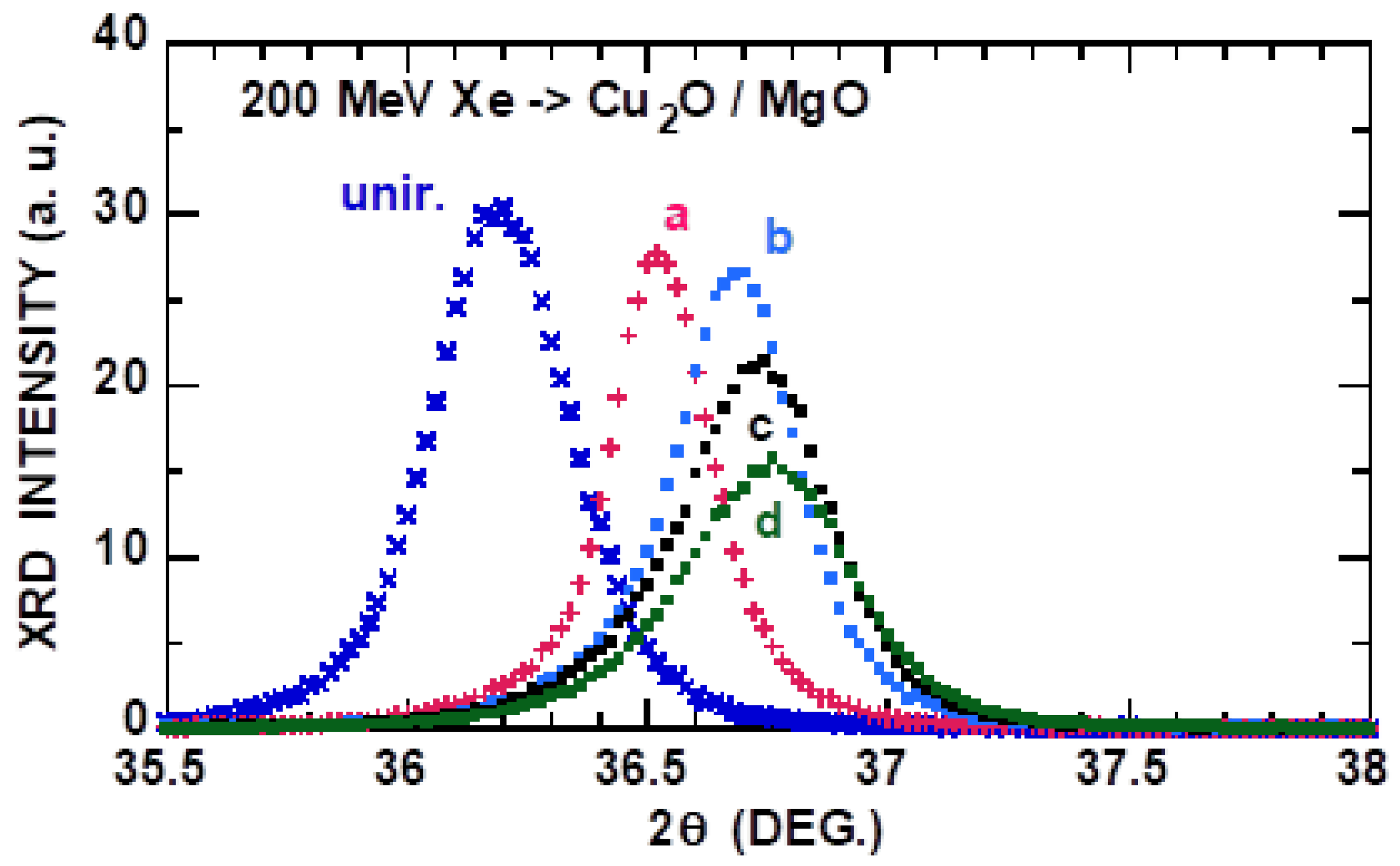
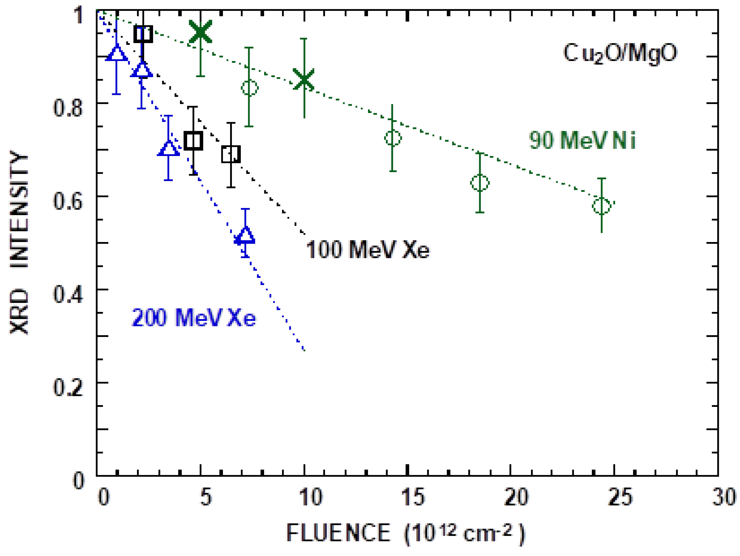
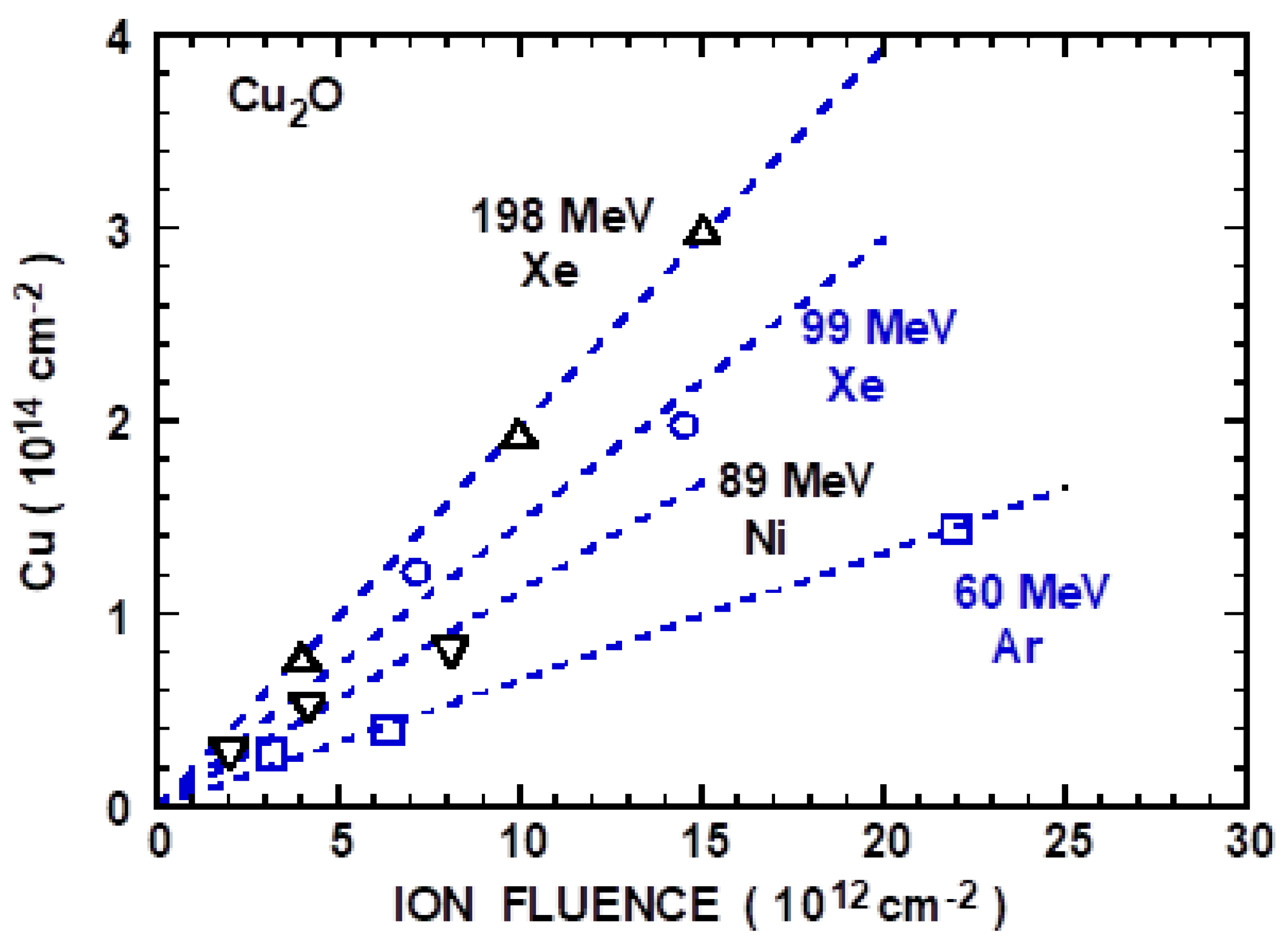
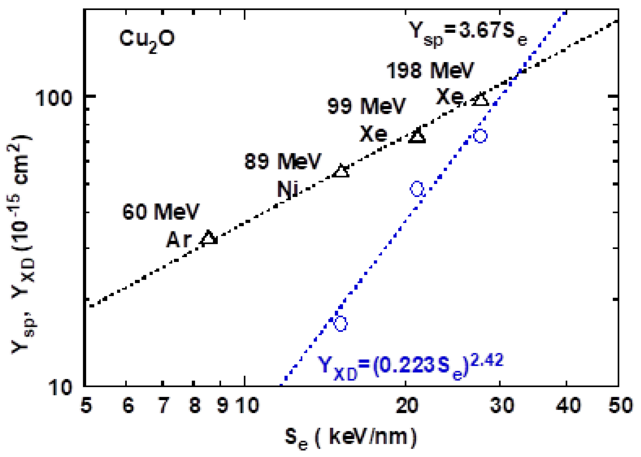
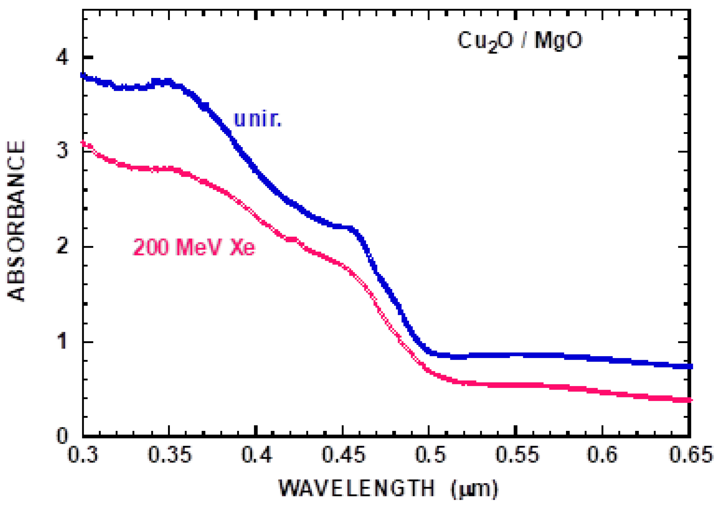
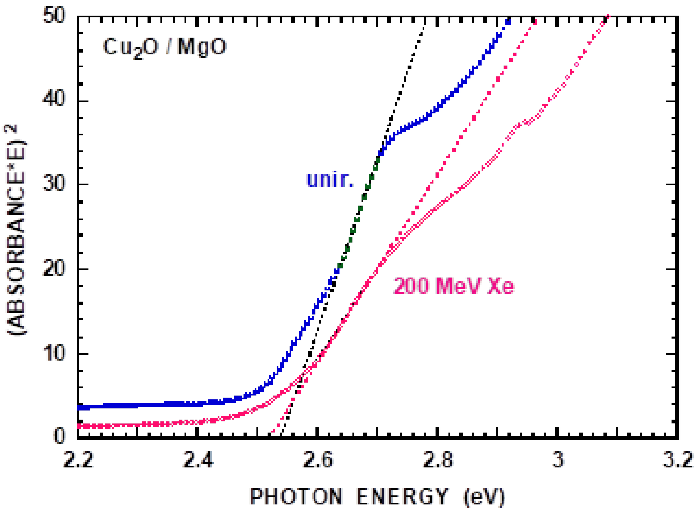
3.1. Cu2O: High-Energy Ion Impact

XRD patterns of Cu2O films are shown in Figure 1 and Figure 2 for irradiation by 200 MeV Xe and 100 MeV Xe ions. It is seen that the XRD intensity decreases with the ion fluence, and the diffraction angle increases. The XRD intensity at a diffraction angle of ~36° (the most intensive (111) diffraction of cubic cuprite), normalized to that of unirradiated films (normalized intensity), is shown in Figure 3 as a function of ion fluence for 90 MeV Ni+10, 100 MeV Xe+14, and 200 MeV Xe+14 ions. It appears that the normalized XRD intensity is proportional to the ion fluence. From the slope, the XRD degradation yield per unit ion fluence (YXD, representing lattice disordering cross-section) is obtained, and the results are provided in Table 2. The linear relationship (Figure 3) can be understood by the idea that the normalized XRD intensity corresponds to 1 − χmin. Here, χmin is the minimum yield of RBS-C due to disordering or amorphization. A saturation formula [49] is often applied to the ion fluence dependence of χminmin = 1 − exp(−AF), A and F being the disordering cross-section and ion fluence, and χmi is proportional to F for low F. Lattice compaction has been observed, and the appreciable change begins at low fluence, as already reported [38]. The decrease in the lattice parameter per unit fluence (YLC) is obtained to be 2.5, 4.3, and 6.8 × 10⁻¹⁵ cm−2 for 90 MeV Ni, 100 MeV Xe, and 200 MeV Xe ions, respectively, with an estimated accuracy of 20%. Se dependence of the lattice parameter change is fitted by a power-law and obtained to be (0.123●Se)1.54. It appears that the Se dependence of YLC is weaker than that of YXD, as described later.
The electronic stopping power (Se*) appropriate for XRD intensity degradation is calculated using TRIM 1997 [17], with the approximation that the appropriate energy (E*) is yielded by the energy at the middle of the film thickness (~50 nm), i.e., Se* = Se(E*) with E* = E(incidence)—Se(E)●50 nm (Table 2). This correction is very close to that in C-foil, employed for sputtering measurements, and thus, the same Se* is adopted for both the XRD intensity degradation and sputtering (Table 2). Correction of Se appears to be less than 1 percent. The areal density of Cu in the C-foil collector vs. ion fluence after revision [15] is shown in Figure 4. It is seen that Cu areal density is proportional to the ion fluence, and from the slope (Cu areal density/ion fluence), the sputtering yields of Cu (YCu) are obtained. Here, the collection efficiency of Cu in the C-foil collector is taken to be 0.3 [38]. The total sputtering yields Ysp of Cu2O equal to 1.5 times YCu, assuming stoichiometric sputtering. Ysp of Cu2O is summarized in Table 2. Comparison of Se dependence of the disordering YXD with that of Ysp is shown in Figure 5. Both YXD and Ysp fit to the power-law. It is seen that YXD has a much stronger dependence than that of Ysp and that of YLC, as mentioned above.
The optical absorption spectra of unirradiated Cu2O and irradiated by 200 MeV Xe at 7.15 × 1012 cm−12 are shown in Figure 6. No appreciable change in optical absorption spectra by the ion irradiation is observed, as reported for 100 MeV Xe ions at 3 × 10⁻¹² cm−2 [38], except for a small reduction of a hump around the optical wavelength of 0.344 µm. The bandgap (Eg) is obtained to be 2.54 and 2.52 eV for Cu2O films of unirradiated and irradiated by 200 MeV Xe at 7.15 × 1012 cm−2 (Figure 7). Here, a relationship is employed: (absorbance × photon energy)2 is proportional to (photon energy—Eg). The present bandgap agrees well with 2.52 eV [50] and 2.51 eV after annealing [51], though a large scatter of the bandgap has been seen, (2–2.38 eV) pointed out in [39] and (2–2.6 eV) [50], and more complications are discussed by Meyer et al. [52]. Aside from the determination of the bandgap, no appreciable change in the bandgap as well as optical absorption is observed for 200 MeV Xe at 7.15 × 1012 cm−2, 90 MeV Ni at 24 × 1012 cm−2, and 100 MeV Xe at 6 × 1012 cm−2, as reported for 100 MeV Xe at 3 × 1012 cm−2 [38]. The result of high-energy ion impact contrasts with that of low-energy ion impact, where Eg deceases with the ion fluence [39], and the difference of the high- and low-energy ion impact will be discussed in the next section. It would be worthwhile to mention that the optical absorbance (OA = Log10(Io/I), Io and I being the incident and transmitted photon intensity) at 344 nm (3.6 eV) appears to be proportional to the film thickness L for unirradiated films. The absorbance coefficient (OA/L) is obtained to be 0.027 nm−1 after subtracting the OA of the MgO substrate (0.065), and the absorption coefficient α (defined by I = Io exp(–αL)) is 6.2 × 105 cm−1. The present absorption coefficient agrees with 6.77 × 105 cm−1 [53]. The OA coefficient is larger by a factor of ~4 than that of doped ZnO [54].

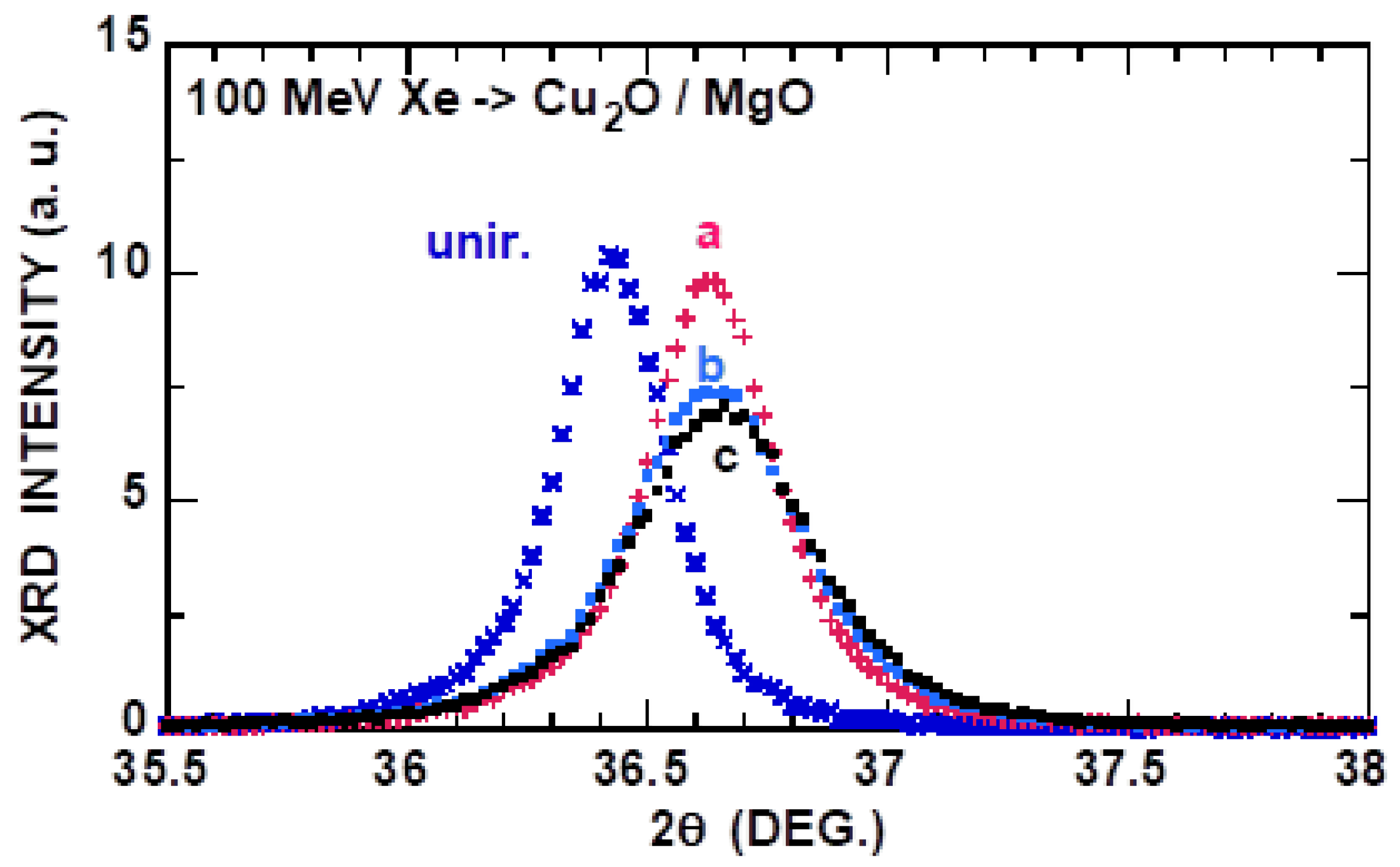
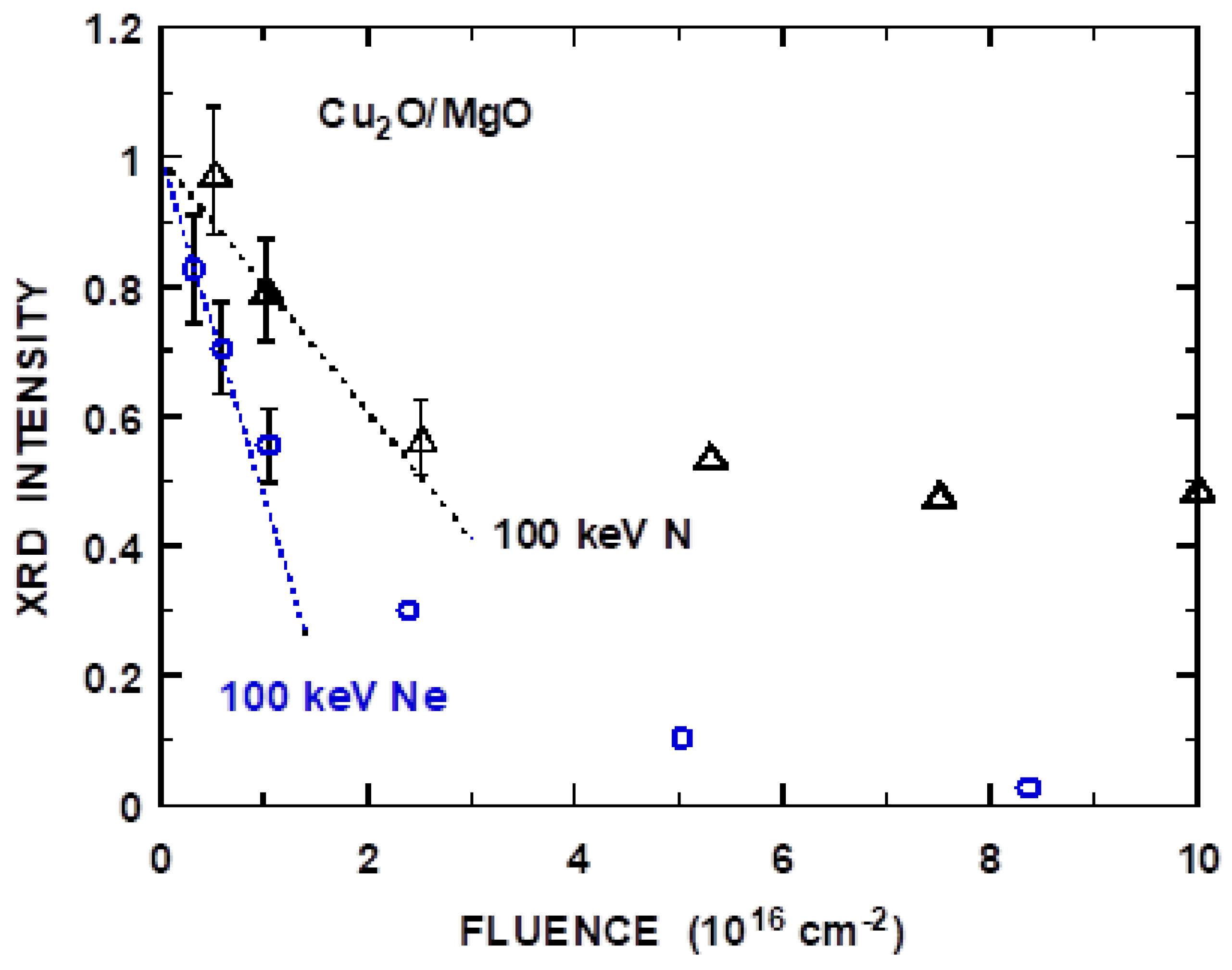
3.2. Cu2O: Low-Energy Ion Impact
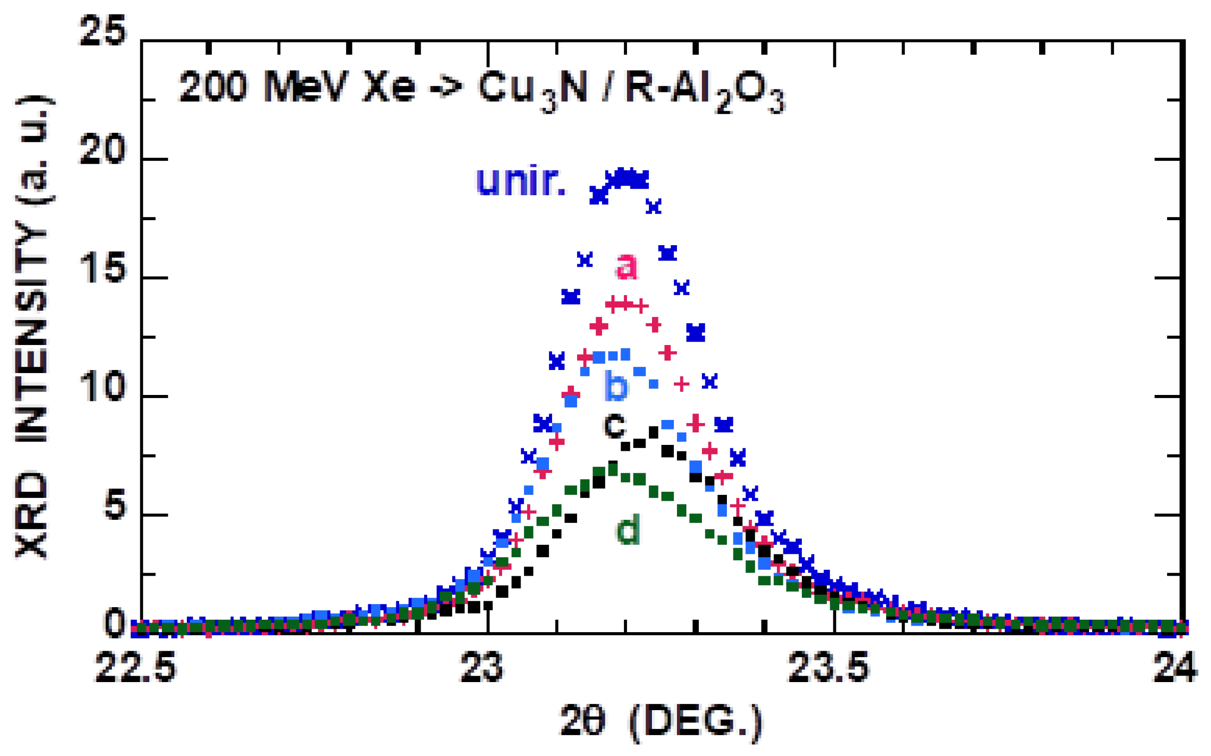
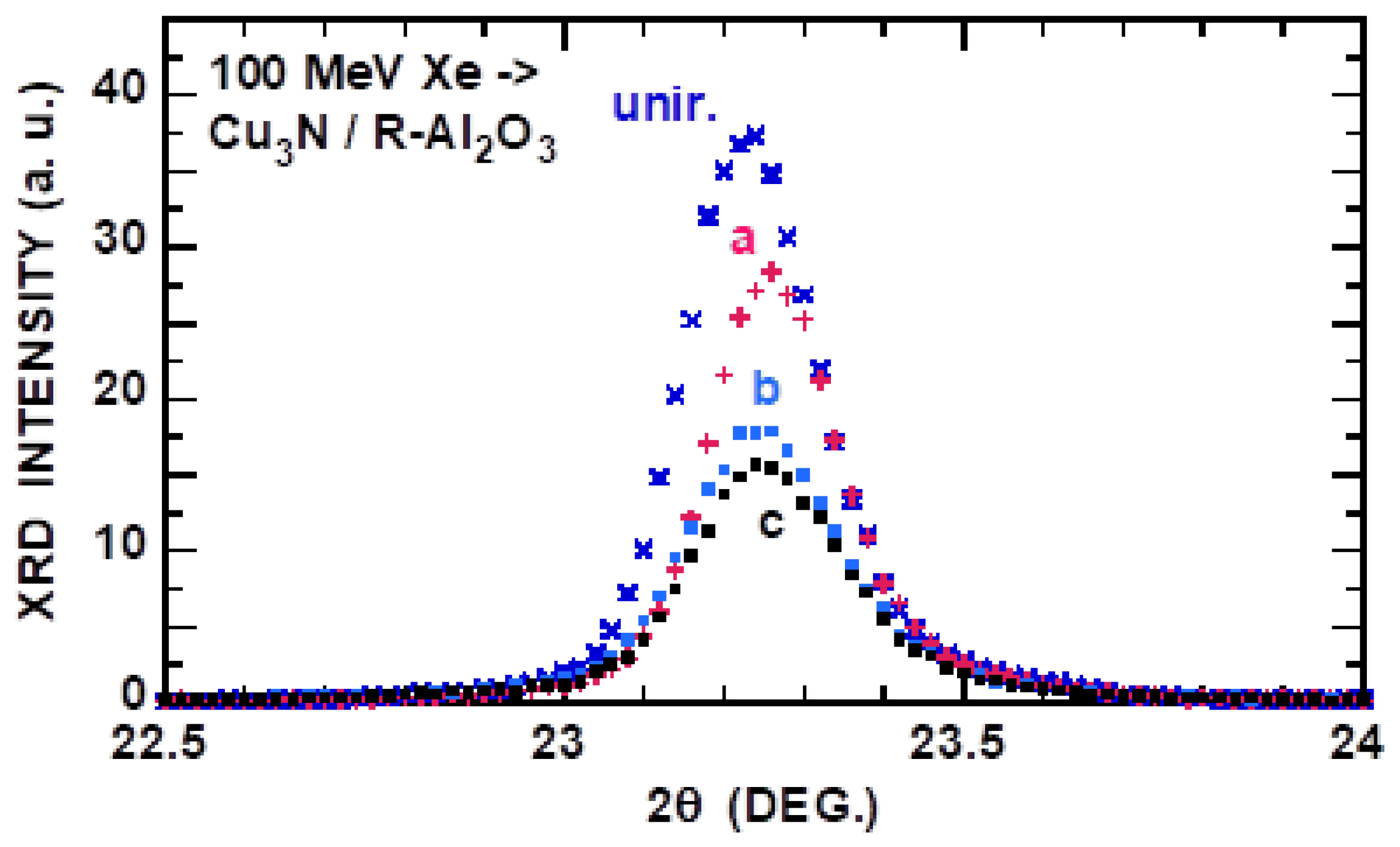
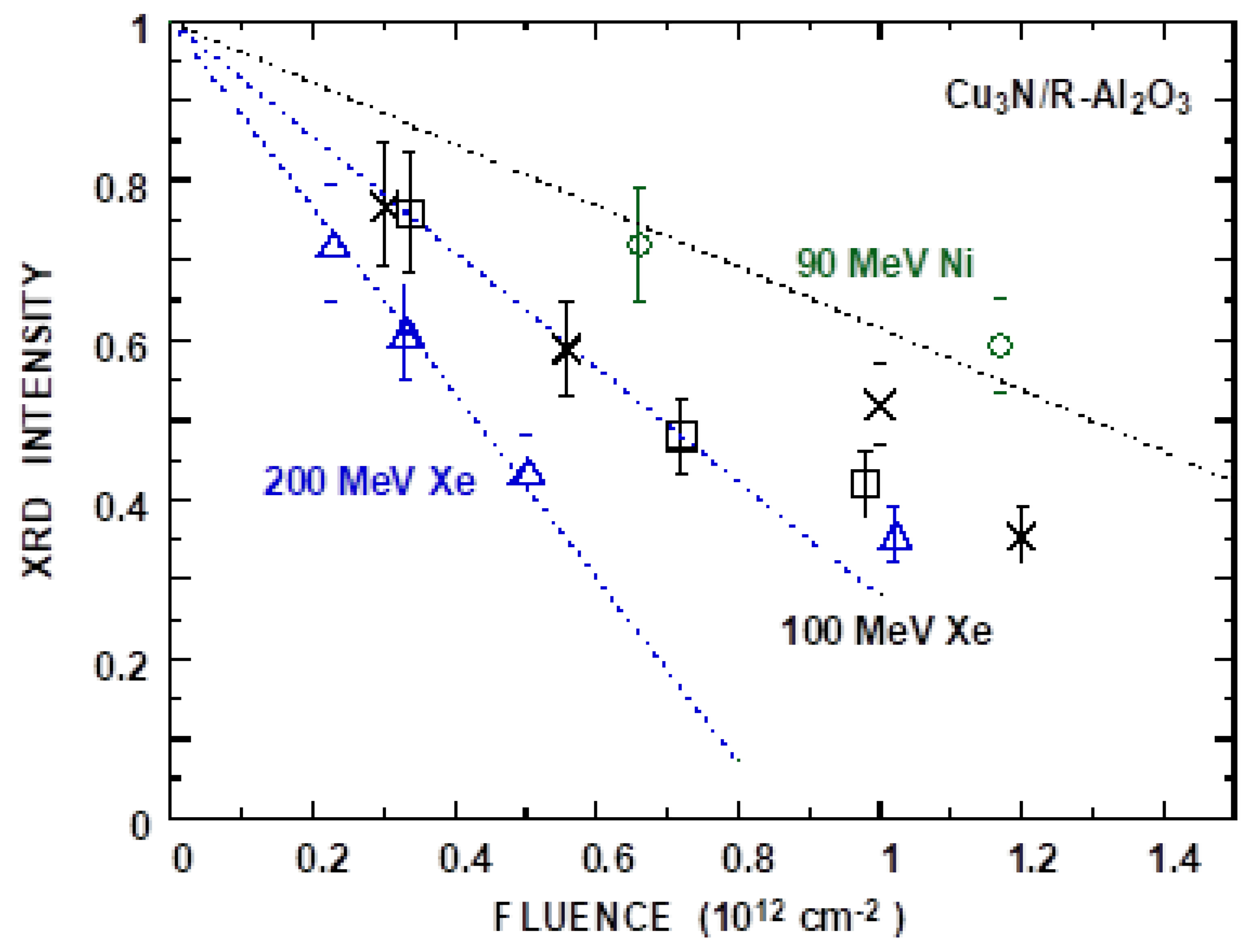
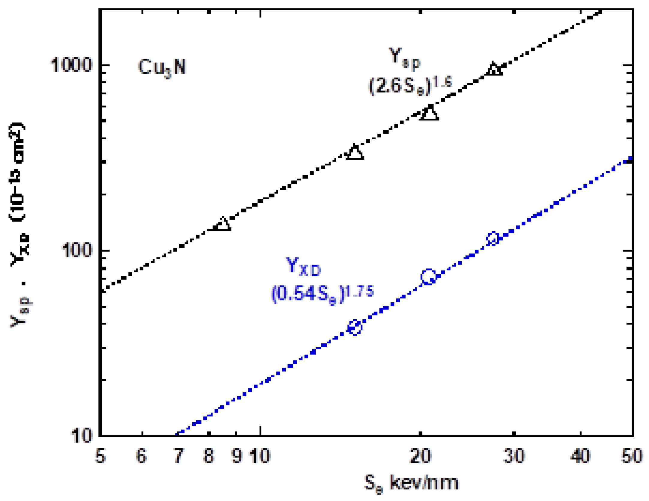
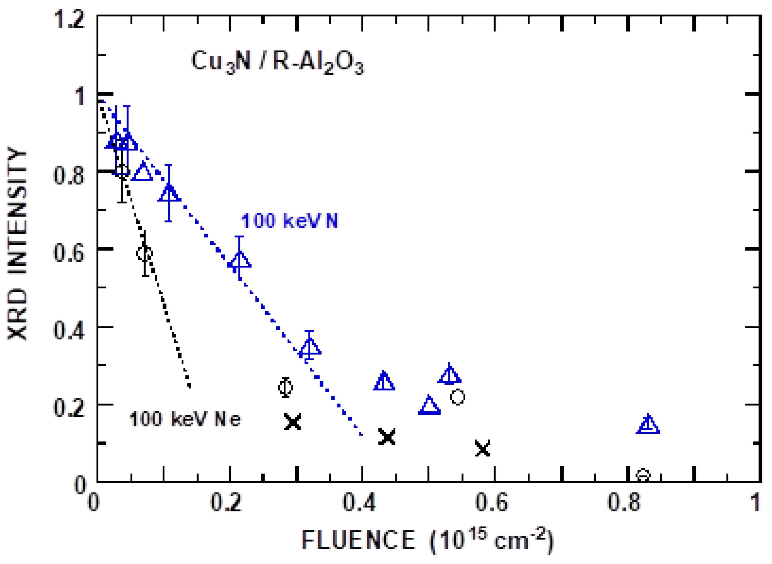
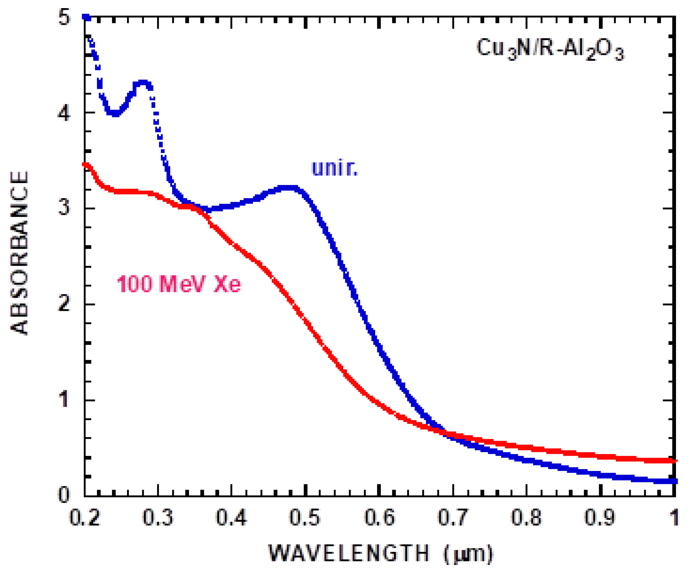
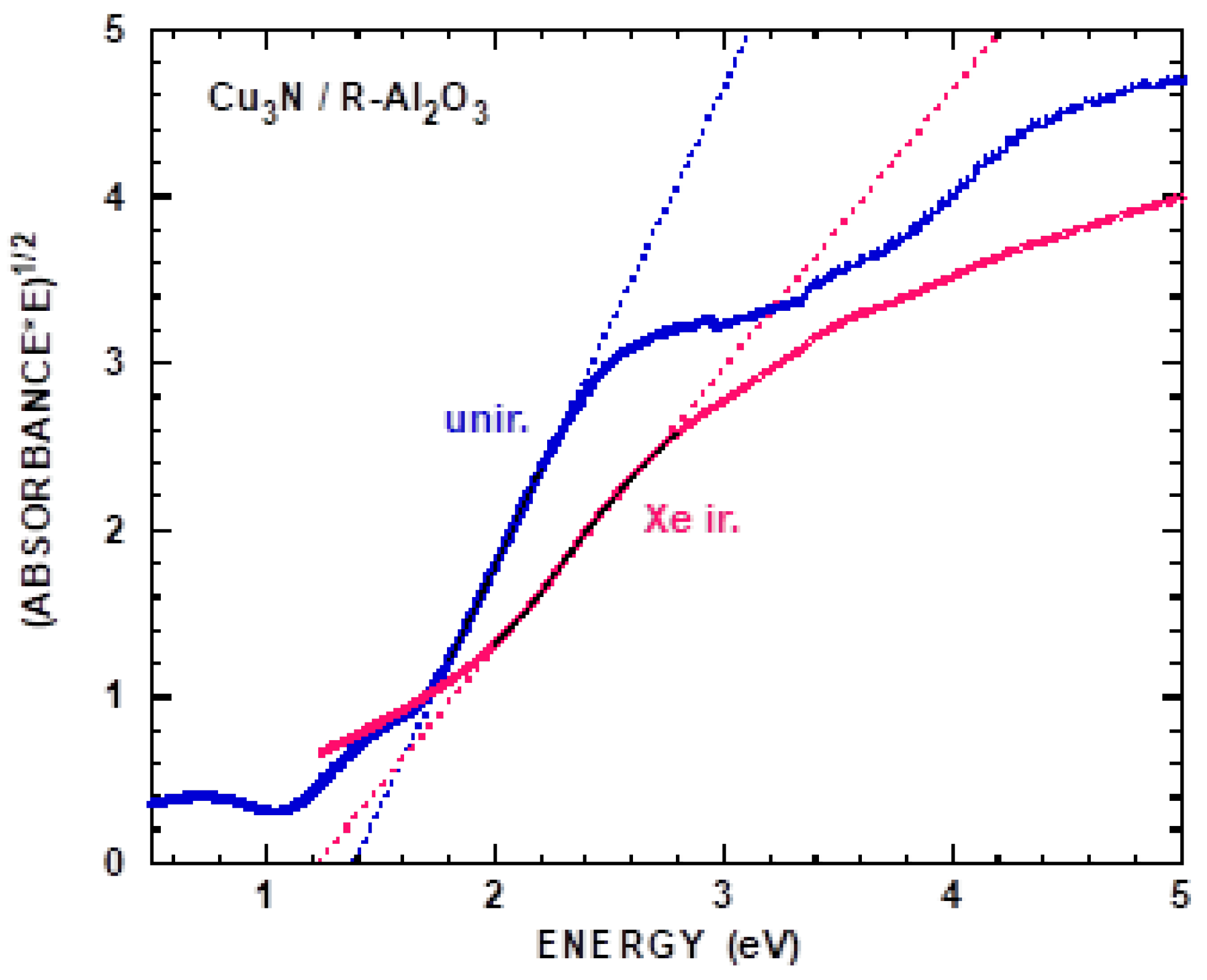
XRD intensity at a diffraction angle of ~36°, normalized to that of unirradiated films (normalized intensity), is shown in Figure 8 as a function of ion fluence for 100 keV N and 100 keV Ne. As in the case of high-energy ion impact (Figure 3), it is found that the normalized XRD intensity decreases proportionally to the ion fluence up to a certain fluence. The slope of the normalized intensity vs. ion fluence is reduced for high fluence, and this could be due to the overlapping effect. From the slope for low fluence, the XRD degradation yield per unit ion fluence (YXD), i.e., lattice disordering cross-section, is obtained, and the results are provided in Table 3. Lattice compaction is ~2% at 10 × 1016 cm−2 for both 100 keV N and Ne, nearly independent of the ion species. Ion, energy, film thickness, projected range (Rp), nuclear and electronic stopping powers averaged over the film thickness (L), and fraction retained of ions in the film (FR) are summarized in Table 3, noting that for L < Rp, FR may play roles in the modifications. Sputtering yields as well as the stopping powers at the surface are also provided in Table 3. The maximum fluence is 10 and 5.2 × 1016 cm−2 for sputtering measurements by 100 keV N and Ne ions, respectively. Averaged stopping powers differ from those in [39], since the electronic energy loss carried by recoils is not taken into account in this study. This choice does not affect the following discussion.
From Table 3, it is found that the ratio of YXD (100 keV Ne) over YXD (100 keV N) is obtained to be 2.68, and this ratio reasonably agrees with the ratio of the average nuclear stopping powers of 2.3. It is also found, as expected, that Ysp (100 keV Ne)/Ysp (100 keV N) is obtained to be 2.08, in good agreement with the nuclear stopping power ratio of 2.3. Here, the so-called α-factor (order of unity, representing the efficiency of the nuclear stopping power contributing to nuclear sputtering [55]) is disregarded. Hence, lattice disordering and sputtering by low-energy ions are nearly proportional to the nuclear stopping power.
No appreciable change in Eg has been observed for high-energy ions. Thus, the observation that the ion fluence dependence of the decrease in the bandgap (Eg) is the same for 100 keV N and Ne ions cannot be explained by nuclear energy deposition or electronic energy deposition. This could be partly due to the implantation effect of low-energy ions, considering the appreciable retained fraction of 11% (100 keV N) and 34% (100 keV Ne), since it has been observed that XRD intensity variation in WNOx films is identical for low-energy (~1 keV) H and D implantation [56]. However, it is not well understood yet at present why there is no ion species dependence of the bandgap decrease in Cu2O with the ion fluence, and more investigations are desired.

3.3. Cu3N

XRD patterns of Cu3N films are shown in Figure 9 and Figure 10 for irradiation by 200 MeV Xe and 100 MeV Xe ions. It is seen that the XRD intensity decreases with the ion fluence, and the diffraction angle remains unchanged. XRD intensity of Cu3N films on R-cut Al2O3 at a diffraction angle of 23° (the most intensive (100) diffraction of cubic structure), normalized to that of unirradiated films (normalized intensity), is shown in Figure 11 as a function of ion fluence for 90 MeV Ni+10, 100 MeV Xe+14, and 200 MeV Xe+14 ions. It is reminded that the Cu phase has been observed at large fluence, meaning decomposition [40]. In this study, only low fluence is of concern, and it is assumed that decomposition does not play a significant role, and this point will be discussed later. It appears that the normalized XRD intensity is proportional to the ion fluence up to certain fluence. From the slope for low fluence, the XRD degradation yield per unit ion fluence (YXD, lattice disordering cross-section) is obtained, and the results are provided in Table 4. A small lattice compaction (−0.2% for 100 MeV Xe at 1013 cm2 or YLC~2 × 10⁻¹⁶ cm2, which is much smaller than that for Cu2O (Section 3.1)) or no appreciable change in the lattice parameter has been observed for the other high-energy ion impacts, including the results shown in Figure 9 and Figure 10. Sputtering yields (Ysp) by high-energy ions are also provided in Table 4. The maximum fluence for the sputtering measurement is 0.8, 2, 1.4, and 1.5 × 1012 cm−2 for 200 MeV Xe, 100 MeV Xe, 90 MeV Ni, and 60 MeV Ar ions. Se dependence of YXD and Ysp is shown in Figure 12.
Normalized XRD intensity as a function of ion fluence for 100 KeV N and 100 keV Ne ions is shown in Figure 13. The XRD degradation yield per unit ion fluence (YXD) is obtained, and the results are provided in Table 5. From Table 5, it is found that the ratio of YXD (100 keV Ne) over YXD (100 keV N) is obtained to be 2.45, and this ratio reasonably agrees with the average nuclear stopping power ratio of 2.2. Hence, the lattice disordering is nearly proportional to the nuclear stopping power. The Cu peak in the XRD appears at 0.82 × 1015 cm−2 (~1 × 1015 cm−2 [40]) for 100 keV Ne ion impact and 4.5 × 1015 cm−2 for 100 keV N ion impact, respectively. Lattice compaction is obtained to be 0.5% at 0.5 × 1015 cm−2 and 0.54% at 0.1 × 1015 cm−2 for 100 keV N and 100 keV Ne ions.
Sputtering yields of Cu3N by 100 keV N and Ne ions are carefully reanalyzed, and the revised yields are obtained to be 3.2 and 7.6, respectively (Table 5). Here, the maximum ion fluence for the sputtering yield evaluation is 6 and 31 × 1015 cm−2 for 100 keV N and Ne, and the fluence is larger than that of the Cu phase appearance in the XRD patterns, as mentioned above. The sputtering yields are much larger than those of Cu2O. The ratio, Ysp (100 keV Ne)/Ysp (100 keV N), is obtained to be 2.38, and this agrees with the nuclear stopping power ratio of 2.22. Again, the so-called α-factor (order of unity, representing the efficiency of the nuclear stopping power contributing to nuclear sputtering [55]) is discarded. As described in Section 2, the estimated macroscopic temperature rise is 40 °C [44]. This temperature rise is smaller than the thermal decomposition temperature, which ranges from 100 to 470 °C [57]. However, the possibility that the large sputtering yields are partly due to decomposition is not ruled out, even though the temperature rise is lower than the decomposition temperature.
The optical absorption spectra are shown in Figure 14 for unirradiated and irradiated Cu3N films by 100 MeV Xe ions. Oscillations are seen in the unirradiated film, and these disappear upon ion irradiation, as in the case of 100 keV Ne impact [40]. The corresponding bandgap is obtained to be 1.38 and 1.22 eV, using the relation where the square root of the absorbance times the photon energy is proportional to the photon energy—bandgap (Figure 15). The optical bandgap modification by ion impact is small. The absorbance of unirradiated films at 0.48 µm (photon energy of 2.58 eV), divided by the film thickness, is obtained to be 0.02 nm−1 after subtracting the OA of Al2O3 (0.065), and the absorption coefficient is found to be 4.6 × 105 cm−1, in reasonable agreement with 5.2 × 105 cm−1 [58].

4. Discussion

The efficiency of electronic energy deposition is compared with that of nuclear energy deposition. Given the linear dependence of the electronic sputtering yield on Se in the case of Cu2O (Section 3.1), the effects of electronic and nuclear energy deposition on sputtering can be well defined for Cu2O. The average of Ysp/Sn (the effect of energy deposition) for two ion species is obtained as 7.9 (kev/nm)−1 from Table 3, and this value is comparable with 3.67 (keV/nm)−1 for electronic sputtering (Figure 3). The energy deposition efficiency is summarized in Table 6. Surprisingly, the results indicate that the energy deposition efficiency for sputtering is comparable within a factor of 2, irrespective of nuclear or electronic energy deposition, even though the effect of electronic energy deposition is an indirect process.
Similarly, the average efficiency of nuclear energy deposition on lattice disordering of Cu2O is obtained to be 1.3 × 10⁻¹⁶ cm2 (keVnm)−1 for low-energy ion impact from Table 3. For high-energy ion impact (Table 2 and Figure 5), a crude estimation of the efficiency of electronic energy deposition is obtained as 1.86 × 10⁻¹⁶ cm2/15 keV/nm = 0.124 × 10⁻¹⁶ cm2 (keV/nm)−1 at Se = 15 keV/nm. The efficiency is obtained as 0.256 × 10⁻¹⁶ cm2(keV/nm)−1 at Se = 25 keV/nm. Hence, the effect of electronic energy deposition is much smaller than that of nuclear energy deposition (less efficient than electronic energy deposition). It might be surprising that for track formation in amorphous SiO2, the same effect of nuclear and electronic energy deposition has been argued [26], in contrast to the above results, noting that the track area and lattice disordering cross-section are similar for SiO2 at high Se [16].
For Cu3N, the average energy deposition efficiency of sputtering for low-energy ions, Ysp/Sn for two ion species, is obtained as 31 (keV/nm)−1 from Table 5, and this value is much larger than that of Cu2O. Because of the super-linear dependence of electronic sputtering on Se for high-energy ion impact on Cu3N, a crude estimation is applied here, as mentioned above. The energy deposition efficiency, Ysp/Se for high-energy ions, is obtained as 23 and 32 (keV/nm)−1 at Se = 15 and 25 keV/nm (Table 4 and Figure 12), and thus, the electronic energy deposition efficiency is comparable with the nuclear energy deposition efficiency for sputtering. The average energy deposition efficiency of lattice disordering for low-energy ions, YXD/Sn for two ion species, is obtained as 14 × 10−15 cm2 (keV/nm)−1 from Table 5, and this value is much larger than that of Cu2O. The energy deposition efficiency, YXD/Se for high-energy ions is obtained as 2.6 and 3.8 × 10⁻¹⁵ cm2 (keV/nm)−1 at Se = 15 and 25 keV/nm (Table 4 and Figure 12), and thus, the electronic energy deposition efficiency is much smaller than the nuclear energy deposition efficiency for lattice disordering. The electronic and nuclear energy deposition efficiencies are comparable for sputtering, and the former is smaller (but less than an order of magnitude) than the latter for lattice disordering.

5. Conclusions

We have measured lattice disordering in polycrystalline Cu2O and Cu3N films using high- and low-energy ions. We find that lattice disordering is caused by electronic excitation for high-energy ion impacts, and the degradation of XRD intensity (lattice disordering cross-section) fits a power-law relationship with electronic stopping power. The degradation of XRD intensity by low-energy ion impact (elastic collisions dominate) is found to be nearly proportional to the nuclear stopping power. We have discussed the efficiency of electronic and nuclear energy deposition on lattice disordering as well as sputtering. It appears that the efficiency of electronic and nuclear energy deposition is comparable for the sputtering of Cu2O and Cu3N. In the case of lattice disordering of Cu2O and Cu3N, we find that the electronic energy deposition efficiency is smaller than the nuclear energy deposition efficiency.

Author Contributions

Conceptualization and writing, N.M.; investigation, M.S., S.O. and B.T. All authors have read and agreed to the published version of the manuscript.

Funding

This research received no external funding.

Institutional Review Board Statement

Not applicable.

Informed Consent Statement

Not applicable.

Data Availability Statement

Data are contained within the article.

Acknowledgments

XRD has been measured using RIGAKU ULTIMA IV and RAD IIc at Radio-isotope Research Center, Nagoya University. Rutherford backscattering spectroscopy and low-energy ion irradiation were performed using AN Van de Graaff and 200 kV ion accelerators, respectively, at Nagoya University. High-energy ion irradiation was done using a TANDEM accelerator at Tokai Research Center, JAEA.

Conflicts of Interest

The authors declare no conflicts of interest.

References

  1. Brown, W.L.; Augustyniak, W.M.; Brody, E.; Cooper, B.; Lanzerotti, L.J.; Ramirez, A.; Evatt, R.; Johnson, R.E. Energy Dependence of the Erosion of H2O Ice Films by H and He Ions. Nucl. Instrum. Methods 1980, 170, 321–325. [Google Scholar] [CrossRef]
  2. Bottiger, J.; Davies, J.A.; L’Ecuyer, J.; Matsunami, N.; Ollerhead, R. Erosion of Frozen-Gas Films by MeV Ions. Radiat. Eff. 1980, 49, 119–124. [Google Scholar] [CrossRef]
  3. Brown, W.L.; Lanzerotti, L.J.; Marcantonio, K.J.; Johnson, R.E.; Reimann, C.T. Sputtering of Ices by High Energy Particle Impact. Nucl. Instrum. Methods B 1986, 14, 392–402. [Google Scholar] [CrossRef]
  4. Mejia, C.; Bender, M.; Severin, D.; Trautmann, C.; Boduch, P.; Bordalo, V.; Domaracka, A.; Lv, X.Y.; Martinez, R.; Rothard, H. Radiolysis and sputtering of carbon dioxide ice induced by swift Ti, Ni and Xe ions. Nucl. Instrum. Methods B 2015, 365, 477–481. [Google Scholar] [CrossRef]
  5. Galli, A.; Vorburger, A.; Wurz, P.; Tulej, M. Sputtering of water ice films: A re-assessment with singly and doubly charged oxygen and argon ions, molecular oxygen, and electrons. Icarus 2017, 291, 36–45. [Google Scholar] [CrossRef]
  6. Qiu, Y.; Griffith, J.E.; Meng, W.J.; Tombrello, T.A. Sputtering of Silicon and its Compounds in the Electronic Stopping Region. Radiat. Eff. 1983, 70, 231–236. [Google Scholar] [CrossRef]
  7. Meins, C.K.; Griffith, J.E.; Qiu, Y.; Mendenhall, M.H.; Seiberling, L.E.; Tombrello, T.A. Sputtering of UF4 by High Energy Heavy Ions. Radiat. Eff. 1983, 71, 13–33. [Google Scholar] [CrossRef]
  8. Bouffard, S.; Duraud, J.P.; Mosbah, M.; Schlutig, S. Angular distribution of the sputtered atoms from UO2 under high electronic stopping power irradiation. Nucl. Instrum. Methods B 1998, 141, 372–377. [Google Scholar] [CrossRef]
  9. Schlutig, S. Contribution a L’etude de la Pulverisation et de L’endommagement du Dioxyde D’uranuim par les Ions Lourds Rapides. Ph.D. Thesis, University of CAEN, Caen, France, 2001. [Google Scholar]
  10. Toulemonde, M.; Assmann, W.; Trautmann, C.; Gruner, F. Jetlike Component in Sputtering of LiF Induced by Swift Heavy Ions. Phys. Rev. Lett. 2002, 88, 057602. [Google Scholar] [CrossRef]
  11. Toulemonde, M.; Assmann, W.; Muller, D.; Trautmann, C. Electronic sputtering of LiF, CaF2, LaF3 and UF4 with 197 MeV Au ions: Is the stoichiometry of atom emission preserved? Nucl. Instrum. Methods B 2017, 406, 501–507. [Google Scholar] [CrossRef]
  12. Matsunami, N.; Sataka, M.; Iwase, A.; Okayasu, S. Electronic excitation induced sputtering of insulating and semiconducting oxides by high energy heavy ions. Nucl. Instrum. Methods B 2003, 209, 288–293. [Google Scholar] [CrossRef]
  13. Toulemonde, M.; Assmann, W.; B.-d’Etat, B.; Bender, M.; Bergmaier, A.; Boduch, P.; Negra, S.D.; Duan, J.; E.-Said, A.S.; Gruner, F.; et al. Sputtering of LiF and other halide crystals in the electronic energy loss regime. Eur. Phys. J. D 2020, 74, 144. [Google Scholar] [CrossRef]
  14. Matsunami, N.; Sataka, M.; Okayasu, S.; Tazawa, M. Electronic sputtering of nitrides by high-energy ions. Nucl. Instrum. Methods B 2007, 256, 333–336. [Google Scholar] [CrossRef]
  15. Matsunami, N.; Okayasu, S.; Sataka, M.; Tsuchiya, B. Electronic sputtering of SiC and KBr by high energy ions. Nucl. Instrum. Methods B 2020, 478, 80–84. [Google Scholar] [CrossRef]
  16. Matsunami, N.; Sataka, M.; Okayasu, S.; Tsuchiya, B. Modification of SiO2, ZnO, Fe2O3 and TiN Films by Electronic Excitation under High Energy Ion Impact. Quantum Beam Sci. 2021, 5, 30. [Google Scholar] [CrossRef]
  17. Ziegler, J.F.; Biersack, J.P.; Littmark, U. The Stopping and Range of Ions in Solids; Pergamon Press: New York, NY, USA, 1985; pp. 1–321. [Google Scholar]
  18. Ziegler, J.F.; Ziegler, M.D.; Biersack, J.P. SRIM-The stopping and range of ions in matter (2010). Nucl. Instrum. Methods B 2010, 268, 1818–1823. [Google Scholar] [CrossRef]
  19. Fleischer, R.L.; Price, P.B.; Walker, R.M. Ion Explosion Spike Mechanism for Formation of Charged-Particle Tracks in Solids. J. Appl. Phys. 1965, 36, 3645–3652. [Google Scholar] [CrossRef]
  20. Itoh, N.; Duffy, D.M.; Khakshouri, S.; Stoneham, A.M. Making tracks: Electronic excitation roles in forming swift heavy ion tracks. J. Phys. Condens. Matter 2009, 21, 474205. [Google Scholar] [CrossRef]
  21. Meftah, A.; Brisard, F.; Costantini, J.M.; Dooryhee, E.; H.-Ali, M.; Hervieu, M.; Stoquert, J.P.; Studer, F.; Toulemonde, M. Track formation in SiO2 quartz and the thermal-spike mechanism. Phys. Rev. B 1994, 49, 12457–12463. [Google Scholar] [CrossRef]
  22. Toulemonde, M.; Bouffard, S.; Studer, F. Swift heavy ions in insulating and conducting oxides: Tracks and physical properties. Nucl. Instrum. Methods B 1994, 91, 108–123. [Google Scholar] [CrossRef]
  23. Afra, B.; Rodriguez, M.D.; Trautmann, C.; Pakarinen, O.H.; Djurabekova, F.; Nordlund, K.; Bierschenk, T.; Giulian, R.; Ridgway, M.C.; Rizza, G. SAXS investigation of the morphology of swift heavy ion tracks in α–quartz. J. Phys. Condens. Matter. 2013, 25, 045006. [Google Scholar] [CrossRef]
  24. Kluth, P.; Pakarinen, O.H.; Djurabekova, F.; Giulian, R.; Ridgway, M.C.; Byrne, A.P.; Nordlund, K. Nanoscale density fluctuations in swift heavy ion irradiated amorphous SiO2. J. Appl. Phys. 2011, 110, 123520. [Google Scholar] [CrossRef]
  25. Benyagoub, A.; Toulemonde, M. Ion tracks in amorphous silica. J. Mater. Res. 2015, 30, 1529–1543. [Google Scholar] [CrossRef]
  26. Toulemonde, M.; Weber, W.J.; Li, G.; Shutthanandan, V.; Kluth, P.; Yang, T.; Wang, Y.; Zhang, Y. Synergy of nuclear and electronic energy losses in ion-irradiation processes: The case of vitreous silicon dioxide. Phys. Rev. B 2011, 83, 054106. [Google Scholar] [CrossRef]
  27. Canut, B.; Benyagoub, A.; Marest, G.; Meftah, A.; Moncoffre, N.; Ramos, S.M.M.; Studer, F.; Thevenard, P.; Toulemonde, M. Swift-uranium-ion-induced damage in sapphire. Phys. Rev. B 1995, 51, 12194–12201. [Google Scholar] [CrossRef]
  28. Khalfaoui, N.; Stoquert, J.P.; Haas, F.; Trautmann, C.; Meftah, A.; Toulemonde, M. Damage creation threshold of Al2O3 under swift heavy ion irradiation. Nucl. Instrum. Methods B 2012, 286, 247–253. [Google Scholar] [CrossRef]
  29. O’Connell, J.H.; Rymzhanov, R.A.; Skuratov, V.A.; Volkov, A.E.; Kirilkin, N.S. Latent tracks and associated strain in Al2O3 irradiated with swift heavy ions. Nucl. Instrum. Methods B 2016, 374, 97–101. [Google Scholar] [CrossRef]
  30. Zinkle, S.J.; Skuratov, V.A.; Hoelzer, D.T. On the conflicting roles of ionizing radiation in ceramics. Nucl. Instrum. Methods B 2002, 191, 758–766. [Google Scholar] [CrossRef]
  31. van Vuuren, A.J.; Ibrayeva, A.D.; Skuratov, V.A.; Zdorovets, M.V. Analysis of the microstructural evolution of silicon nitride irradiated with swift Xe ions. Ceram. Int. 2020, 46, 7155–7160. [Google Scholar] [CrossRef]
  32. Kitayama, T.; Morita, Y.; Nakajima, K.; Narumi, K.; Saitoh, Y.; Matsuda, M.; Sataka, M.; Tsujimoto, M.; Isoda, S.; Toulemonde, M.; et al. Formation of ion tracks in amorphous silicon nitride films with MeV C60 ions. Nucl. Instrum. Methods B 2015, 356–357, 22–27. [Google Scholar] [CrossRef]
  33. Mota-Santiago, P.; Vazquez, H.; Bierschenk, T.; Kremer, F.; Nadzri, A.; Schauries, D.; Djurabekova, F.; Nordlund, K.; Trautmann, C.; Mudie, S.; et al. Nanoscale density variations induced by high energy heavy ions in amorphous silicon nitride and silicon dioxide. Nanotechnology 2018, 29, 144004. [Google Scholar] [CrossRef] [PubMed]
  34. Kucheyev, S.O.; Timmers, H.; Zou, J.; Williams, J.S.; Jagadish, C.; Li, G. Lattice damage produced in GaN by swift heavy ions. J. Appl. Phys. 2004, 95, 5360–5365. [Google Scholar] [CrossRef]
  35. Mansouri, S.; Marie, P.; Dufour, C.; Nouet, G.; Monnet, I.; Lebius, H.; Benamara, Z.; Al-Douri, Y. Swift heavy ion effects in gallium nitride. Int. J. Nanoelectron. Mater. 2008, 1, 101–106. [Google Scholar]
  36. Sall, M.; Monnet, I.; Moisy, F.; Grygiel, C.; J.-Leclerc, S.; Della-Negra, S.; Toulemonde, M.; Balanzat, E. Track formation in III-N semiconductors irradiated by swift heavy ions and fullerene and re-evaluation of the inelastic thermal spike model. J. Mater. Sci. 2015, 50, 5214–5227. [Google Scholar] [CrossRef]
  37. Kamarou, A.; Wesch, W.; Wendler, E.; Undisz, A.; Rettenmayr, M. Swift heavy ion irradiation of InP: Thermal spike modeling of track formation. Phys. Rev. B 2006, 73, 184107. [Google Scholar] [CrossRef]
  38. Matsunami, N.; Sataka, M.; Okayasu, S.; Ishikawa, N.; Tazawa, M.; Kakiuchida, H. High-energy ion irradiation effects on atomic structures and optical properties of copper oxide and electronic sputtering. Nucl. Instrum. Methods B 2008, 266, 2986–2989. [Google Scholar] [CrossRef]
  39. Matsunami, N.; Fukuoka, O.; Tazawa, M.; Kakiuchida, H.; Sataka, M. Electronic structure modifications of cuprous-oxide films by ions. Surf. Coat. Technol. 2009, 203, 2642–2645. [Google Scholar] [CrossRef]
  40. Matsunami, N.; Kakiuchida, H.; Tazawa, M.; Sataka, M.; Sugai, H.; Okayasu, S. Electronic and atomic structure modifications of copper nitride films by ion impact and phase separation. Nucl. Instrum. Methods B 2009, 267, 2653–2656. [Google Scholar] [CrossRef]
  41. Joint Committee on Powder Diffraction Standards (JCPDS) 50667 (Cu2O) and 21156 (Cu3N).
  42. Lide, D.R. (Ed.) CRC Handbook of Chemistry and Physics, 84th ed.; CRC Press: Boca Raton, FL, USA, 2003. [Google Scholar]
  43. Storm, E.; Israel, H.I. Photon Cross Sections from 1 keV to 100 MeV for Elements Z = 1 to Z = 100. Nucl. Data Tables A 1970, 7, 565–681. [Google Scholar] [CrossRef]
  44. Matsunami, N.; Yajima, T.; Iwahara, H. Permeation of implanted deuterium through SrCeO3 (5% Yb). Nucl. Instrum. Methods B 1992, 65, 278–281. [Google Scholar] [CrossRef]
  45. Matsunami, N.; Sataka, M.; Okayasu, S.; Tsuchiya, B. Charge State Effect of High Energy Ions on Material Modification in the Electronic Stopping Region. Atoms 2021, 9, 36. [Google Scholar] [CrossRef]
  46. DuBois, R.D.; Santos, A.C.F.; Olson, R.E. Scaling laws for electron loss from ion beams. Nucl. Instrum. Methods A 2005, 544, 497–501. [Google Scholar] [CrossRef]
  47. DuBois, R.D.; Santos, A.C.F. Target-Scaling Properties for Electron Loss by Fast Heavy Ions. In Atomic Processes in Basic and Applied Physics; Shevelko, V., Tawara, H., Eds.; Springer: Berlin/Heidelberg, Germany, 2012; Chapter 8; pp. 185–209. [Google Scholar]
  48. Rodrigues, G.C.; Indelicato, P.; Santos, J.P.; Patte, P.; Parente, F. Systematic calculation of total atomic energies of ground state configurations. At. Data Nucl. Data Tables 2004, 86, 117–233. [Google Scholar] [CrossRef]
  49. Weber, W.J. Models and mechanisms of irradiation-induced amorphization in ceramics. Nucl. Instrum. Methods B 2000, 166–167, 98–106. [Google Scholar] [CrossRef]
  50. Chen, A.; Long, H.; Li, X.; Li, Y.; Yang, G.; Lu, P. Controlled growth and characteristics of single-phase Cu2O and CuO films by pulsed laser deposition. Vacuum 2009, 83, 927–930. [Google Scholar] [CrossRef]
  51. Wang, Y.; Miska, P.; Pilloud, D.; Horwat, D.; Mucklich, F.; Pierson, J.F. Transmittance enhancement and optical band gap widening of Cu2O thin films after air annealing. J. Appl. Phys. 2014, 115, 073505. [Google Scholar] [CrossRef]
  52. Meyer, B.K.; Polity, A.; Reppin, D.; Becker, M.; Hering, P.; Klar, P.J.; Sander, T.; Reindl, C.; Benz, J.; Eickhoff, M.; et al. Binary copper oxide semiconductors: From materials towards devices. Phys. Status Solidi B 2012, 249, 1487–1509. [Google Scholar] [CrossRef]
  53. Malerba, C.; Biccari, F.; Ricardo, C.L.A.; D’Incau, M.; Scardi, P.; Mittiga, A. Absorption coefficient of bulk and thin film Cu2O. Sol. Energy Mater. Sol. Cells 2011, 95, 2848–2854. [Google Scholar] [CrossRef]
  54. Matsunami, N.; Itoh, M.; Kato, M.; Okayasu, S.; Sataka, M.; Kakiuchida, H. Ion induced modifications of Mn-doped ZnO films. Nucl. Instrum. Methods B 2015, 365, 191–195. [Google Scholar] [CrossRef]
  55. Matsunami, N.; Yamamura, Y.; Itikawa, Y.; Itoh, N.; Kazumata, Y.; Miyagawa, S.; Morita, K.; Shimizu, R.; Tawara, H. Energy Dependence of the Ion-Induced Sputering Yields of Monatomic Solids. Atom. Data Nucl. Data Tables 1984, 31, 1–80. [Google Scholar] [CrossRef]
  56. Matsunami, N.; Ohno, N.; Tokitani, M.; Tsuchiya, B.; Sataka, M.; Okayasu, S. Modifications of WNOx films by keV D and H ions. Surf. Coat. Technol. 2020, 394, 125798. [Google Scholar] [CrossRef]
  57. Pierson, J.F. Structure and properties of copper nitride films formed by reactive magnetron sputtering. Vacuum 2002, 66, 59–64. [Google Scholar] [CrossRef]
  58. Borsa, D.M.; Boerma, D.O. Growth, structural and optical properties of Cu3N films. Surf. Sci. 2004, 548, 95–105. [Google Scholar] [CrossRef]
Figure 1. XRD patterns of (111) diffraction plane for unirradiated (x, blue) and irradiated Cu2O films by 200 MeV Xe ions at 0.95 (a, red), 2.16 (b, light blue), 3.44 (c, black), and 7.15 × 1012 cm−2 (d, green).
Qubs 08 00012 g001
Figure 2. XRD patterns similar to Figure 1, except for 100 MeV Xe ions at 2.23 (a, red), 4.67 (b, light blue), and 6.47 × 1012 cm−2 (c, black).
Qubs 08 00012 g002
Figure 3. XRD intensity from (111) diffraction plane 36–37°, normalized to unirradiated films of Cu2O as a function of ion fluence for 90 MeV Ni (o, x), 100 MeV Xe (), and 200 MeV Xe (∆) ions. Data of 90 MeV Ni (x) from [38]. Linear fit is indicated by dotted lines. An estimated error of XRD intensity is 10%, as indicated by error bars.
Qubs 08 00012 g003
Figure 4. Areal density of sputtered Cu from Cu2O on MgO substrate collected in carbon foil vs. ion fluence for 60 MeV Ar (□), 89 MeV Ni (∇), 99 MeV Xe (o), and 198 MeV Xe (∆) ions. An estimated error of areal density is 10%.
Qubs 08 00012 g004
Figure 5. XRD intensity degradation YXD (10−15 cm2) (o) and sputtering yield Ysp (∆) as a function of electronic stopping power, Se(keV/nm). Also shown is power-law fit: YXD = (0.223Se)2.42 and Ysp = 3.67 Se. An estimated error of YXD and Ysp is 10%.
Qubs 08 00012 g005
Figure 6. Optical absorption spectra of Cu2O for unirradiated Cu2O (blue) and Cu2O irradiated by 200 MeV Xe at 7.2 × 1012 cm−2 (red).
Qubs 08 00012 g006
Figure 7. Square of optical absorbance times photon energy vs. photon energy of Cu2O for unirradiated Cu2O (blue) and Cu2O irradiated by 200 MeV Xe at 7.2 × 1012 cm−2 (red), illustrating the bandgap.
Qubs 08 00012 g007
Figure 8. XRD intensity from (111) diffraction plane at 36–37°, normalized to unirradiated films of Cu2O as a function of ion fluence for 100 keV N (∆) and 100 keV Ne (o). Data of 100 keV Ne from [39]. Linear fit is indicated by dotted lines. An estimated error of XRD intensity is 10%, as indicated by error bars.
Qubs 08 00012 g008
Figure 9. XRD patterns of (100) diffraction plane for unirradiated (blue) and irradiated Cu3N films by 200 MeV Xe ions at 0.226 (a, red), 0.33 (b, light blue), 0.5 (c, black), and 1.02 × 1012 cm−2 (d, green).
Qubs 08 00012 g009
Figure 10. XRD patterns similar to Figure 9, except for 100 MeV Xe ions at 0.336 (a, red), 0.72 (b, light blue), and 0.98 × 1012 cm−2 (c, black).
Qubs 08 00012 g010
Figure 11. XRD intensity from (100) diffraction plane at nearly 23°, normalized to unirradiated films of Cu3N as a function of ion fluence for 90 MeV Ni (o), 100 MeV Xe (□, x), and 200 MeV Xe (∆) ions. Data of 100 MeV Xe (x) from [40]. Linear fit is indicated by dotted lines. The estimated error of XRD intensity is 10%, as indicated by error bars.
Qubs 08 00012 g011
Figure 12. XRD intensity degradation YXD (10−15 cm2) (o) and sputtering yield Ysp (∆) as a function of electronic stopping power, Se (keV/nm). Also shown is power-law fit: YXD (10−15 cm2) = (0.54Se)1.75 and Ysp = (2.6 Se)1.6. An estimated error of YXD and Ysp is 10%.
Qubs 08 00012 g012
Figure 13. XRD intensity from (100) diffraction plane at nearly 23°, normalized to unirradiated films of Cu3N as a function of ion fluence for 100 keV N (o) and 100 keV Ne (∆, x) ions. Data of 100 keV Ne (x) from [40]. Linear fit is indicated by dotted lines. An estimated error of XRD intensity is 10%, as indicated by error bars.
Qubs 08 00012 g013
Figure 14. Optical absorption spectra of Cu3N for unirradiated (blue) and irradiated Cu3N by 100 MeV Xe at 1.2 × 1012 cm−2 (red).
Qubs 08 00012 g014
Figure 15. Square root of optical absorbance times photon energy vs. photon energy of Cu3N for unirradiated Cu3N (blue) and irradiated Cu3N by 100 MeV Xe at 1.2 × 1012 cm−2 (red), illustrating the bandgap.
Qubs 08 00012 g015
Table 1. Ion, energy (MeV), first ionization potential of ion (IP, eV), effective number of removable electrons (Neff), single-electron loss cross-section (σ1L, 10−16 cm2), characteristic length (LEQ, nm) attaining the equilibrium charge for Cu2O and Cu3N. IP is taken from [42,48], and σ1L is taken from [46,47].
IonE
(MeV)
IP
(eV)
Neffσ1L
(10−16 cm2)
LEQ (Cu2O)
(nm)
LEQ (Cu3N)
(nm)
58Ni+109032180.358(Cu) 4.64.6
0.152(O)
0.139(N)
136Xe+14100343120.376(Cu)4.44.4
0.159(O)
0.146(N)
136Xe+14200343120.392(Cu)4.24.2
0.166(O)
0.152(N)
Table 2. XRD and sputtering data of Cu2O films for high-energy ions. Ion, incident energy (E in MeV), XRD intensity degradation (YXD), sputtering yield (YSP), appropriate energy E* (MeV) considering the energy loss in the film or carbon foil collector, electronic stopping power (Se*), nuclear stopping power (Se*) in keV/nm at E*. The deviation ∆Se* = (Se*/Se(E) − 1) × 100 is also provided. Stopping powers are calculated using TRIM1997. Se* calculated using SRIM2013 is provided in the parenthesis after Se* (TRIM1997).
IonE
(MeV)
YXD
(10−15 cm2)
YSPE*
(MeV)
Se*
(keV/nm)
Sn*
(keV/nm)
∆Se*
(%)
136Xe2007398.8198 27.55 (27.59)0.115−0.24
136Xe1004873.89920.95 (21.61)0.202−0.62
58Ni9016.55689 15.12 (13.98)0.0318+0.026
40Ar60 33608.52 (8.45)0.0140
Table 3. XRD and sputtering data of Cu2O films for low-energy ions. Ion, incident energy (E, keV), film thickness L (nm), projected range (Rp nm), nuclear (<Sn>) and electronic (<Se>) stopping powers averaged over film thickness relevant to XRD intensity degradation (YXD), YXD(10−16 cm2), retained fraction of ions in film (FR %), nuclear (Sn) and electronic (Se) stopping powers at surface relevant to sputtering, sputtering yield (YSP). Projected range, stopping powers, and retained fraction are calculated using TRIM1997. Sputtering data from [39].
IonE
(keV)
L
(nm)
Rp
(nm)
<Sn>
(keV/nm)
<Se>
(keV/nm)
YXD
(10−16 cm2)
FR
(%)
Sn
(keV/nm)
Se
(keV/nm)
YSP
N100761520.160.380.19611 0.1080.430.9
Ne100991180.370.290.525340.2510.4081.87
Table 4. XRD and sputtering data of Cu3N/R-Al2O3 films for high-energy ions. Ion, incident energy (E in MeV), XRD intensity degradation (YXD), sputtering yield (YSP), appropriate energy E* (MeV) considering the energy loss in the film or carbon foil collector, electronic stopping power (Se*), nuclear stopping power (Sn*) in keV/nm at E*. The deviation ∆Se* = (Se*/Se(E) − 1) × 100 is also provided. Stopping powers are calculated using TRIM1997. Se* calculated using SRIM2013 is provided in the parenthesis after Se* (TRIM1997).
IonE
(MeV)
YXD
(10−15 cm2)
YSPE*
(MeV)
Se*
(keV/nm)
Sn*
(keV/nm)
∆Se*
(%)
136Xe200116960198 27.37 (27.71)0.116−0.24
136Xe100725569920.74 (21.64)0.204−0.62
58Ni9038.534289 15.03 (14.04)0.0321+0.02
40Ar60 142608.47 (8.49)0.01420
Table 5. XRD and sputtering data of Cu3N films for low-energy ions. Ion, incident energy (E, keV), film thickness L (nm), projected range (Rp nm), nuclear (<Sn>) and electronic (<Se>) stopping powers (keV/nm) averaged over the film thickness relevant to XRD intensity degradation (YXD), YXD(10−15 cm2), retained fraction of ions in film (FR %), nuclear (Sn) and electronic (Se) stopping powers at surface relevant to sputtering, sputtering yield (YSP). Rp, FR, and stopping powers are calculated using TRIM1997.
IonE
(keV)
L
(nm)
Rp
(nm)
<Sn>
(keV/nm)
<Se>
(keV/
nm)
YXD
(10−15 cm2)
FR
(%)
Sn
(keV/
nm)
Se
(keV/
nm)
YSP
N100881500.1650.3812.2170.1060.3633.2
Ne100881160.3630.3035.4280.2360.2897.6
Table 6. A summary of the energy deposition efficiency. RXD = (YXD/Se)/(YXD/Sn) and Rsp = (Ysp/Se)/(Ysp/Sn) are the efficiency ratios for lattice disordering and sputtering due to electronic and nuclear energy deposition. The values in the parenthesis are Se (keV/nm), used for YXD/Se evaluation.
SampleYXD/Se
(10−16 cm2) (keV/nm)−1
YXD/SnRXDYsp/SeYsp/SnRsp
Cu2O0.124 (15)1.30.095 3.677.90.46
0.256 (25) 0.20
Cu3N26 (15)1400.1923 (15)310.7
38 (25) 0.2732 (25) 1.0
Disclaimer/Publisher’s Note: The statements, opinions and data contained in all publications are solely those of the individual author(s) and contributor(s) and not of MDPI and/or the editor(s). MDPI and/or the editor(s) disclaim responsibility for any injury to people or property resulting from any ideas, methods, instructions or products referred to in the content.

