Proceeding Paper

Multilayer Micromechanics Process with Thick Functional Layers (EPyC40) †

1
Robert Bosch GmbH, D-72762 Reutlingen, Germany
2
Department of Electrical Engineering and Information Technology and Fraunhofer Institute for Electronic Nano Systems ENAS Chemnitz, Technical University Chemnitz-Zwickau, D-09107 Chemnitz, Germany
*
Author to whom correspondence should be addressed.
Presented at the Eurosensors 2017 Conference, Paris, France, 3–6 September 2017.
Proceedings 2017, 1(4), 296; https://doi.org/10.3390/proceedings1040296
Published: 17 August 2017
(This article belongs to the Proceedings of Proceedings of Eurosensors 2017, Paris, France, 3–6 September 2017)

Abstract

:
The EPyC process (Epi-Poly-Cycle) (by Robert Bosch GmbH) opens up unique opportunities for manufacturing complex 3D MEMS structures having high effectiveness in small space. EPyC40 is an EPyC process with up to 40 μm thick polysilicon layers and sacrificial silicon technique. For successful manufacturing a 40 μm EPyC the epitaxial polysilicon layer must be electrically and mechanically optimized. A vertical deep trench patterns the functional and sacrificial areas. A passivation must be deposited homogeneously and has to be tight and robust towards silicon-etching gases. For more than one cycle it is necessary to tailor the layer stress of the epitaxial polysilicon and the wafer-bow. The full process for stacking up 5 EPyC cycles with two 40 μm epitaxial polysilicon layers was investigated in detail. A true 3D MEMS device providing high z deflection by use of a vertical comb drive with 40 μm electrodes was built up successfully to prove the feasibility of the EPyC process.

1. Introduction

The possibilities for manufacturing of 3D MEMS with high freedom of movement, in particular in the z-direction with a small lateral extension of the component, are very limited [1,2,3]. The EPyC process is an innovative highly flexible MEMS-process and offers a wide range of application opportunities [4]. The special feature of the EPyC process is the use of silicon as a functional and sacrificial layer. This makes it possible to generate high volume sacrificial structures of up to 100 microns thickness. It is based on cyclic deposition of epitaxial poly-silicon and oxide. The silicon is structured to separate sacrificial silicon from functional silicon. The trenches are refilled with oxide and the functional structure is finally released using SF6 plasma and gaseous XeF2. The oxide passivation is cleaned off the surfaces with HF vapor phase etching. EPyC40 is an EPyC process with 40 μm thick poly-silicon layers. For successful manufacturing of a 40 μm EPyC the epitaxial poly-silicon layer must be electrically and mechanically optimized. A vertical deep trench with high aspect ratio is needed. The passivation must be deposited homogeneously and has to be tight and robust towards silicon-etching gases. For more than one cycle it is necessary to tailor the wafer bow. In this paper the complete process of a vertical comb structure with 40 μm high electrodes will be studied in all details. To build up the comb structure the EPyC process is cycled 5 times in total.

2. Vertical Comb Drive Realized by EPyC Process

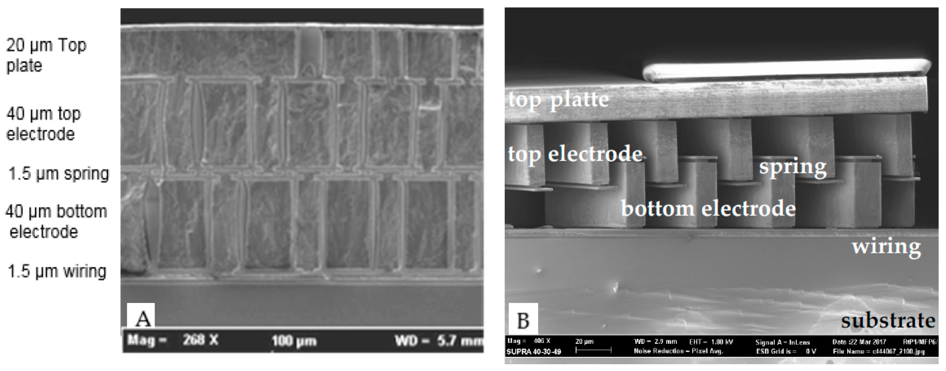
The fabrication sequence of a vertical comb structure using a thick epitaxial polysilicon sacrificial layer is shown in Figure 1. The comb structure consists of 2 × 40 μm high electrodes (top and bottom), a wiring-layer of 1.5 μm, a spring of 1.5 μm and a top plate of 20 μm thickness.
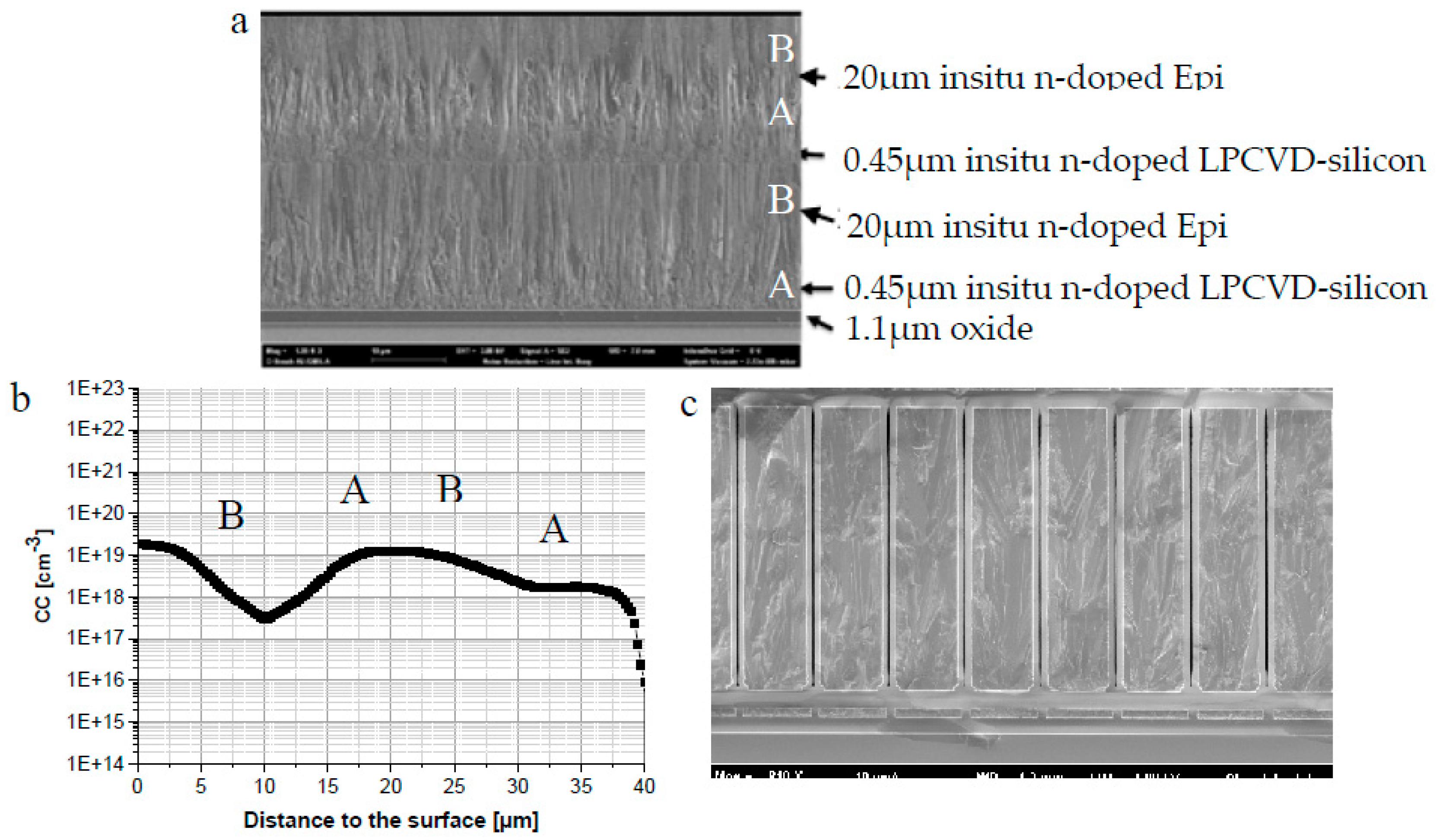
Starting from a standard 8 inch silicon substrate, a 2.5 μm thermal oxide is grown. The oxide is used as an insulator and a vertical etch stop during sacrificial etching. Onto this oxide a 5 μm thick n-insitu doped epitaxial polysilicon layer 1 (Epi1) is deposited. The Epi1 starts from a thin polysilicon seed layer and is grown in a single wafer cold wall reactor. The silicon layer is planarised chemical-mechanical polishing to a final thickness of 1.5 μm. To improve the conductivity of this layers a doping process with POCl3 is used. A 1.4 μm single gap size mask defines buried interconnectors beneath the movable comb structure. The polysilicon layer is structured with a deep reactive ion etching process (DRIE). In the next step a 2.2 μm thick TEOS based oxide with good step coverage is deposited. This oxide acts as an insulator between the interconnectors and as lateral etch stop during sacrificial etching. The oxide is patterned by a CF4 oxide RIE process to form contact holes to finish thefirst complete EPyC cycle (1.5 μm). Subsequently the second EPyC cycle follows with a 40 μm Epi. The optimized stack consists of two 20 μm insitu n-doped Epi layers (A) and two separate insitu n-doped LPCVD-silicon layers of 450 nm thickness (B). The layer sequence is B-A-B-A (Figure 2a). Thus top and bottom of each thick 20 μm layer is in direct contact to a thin highly doped poly-layer [5].
The 40 μm stack can thus be deposited with a very high charge carrier concentration of 1017–1019 cm−3 as shown in Figure 2b. The structuring of 40 μm thick silicon-stack was performed by deep reactive ion etching (DRIE) a 1.4 μm single gap size mask was used. The DRIE-process optimized towards the high aspect ratio of ~1:28 showed only 600 nm one sided etch loss and minimal notching. The 2.5 μm TEOS based oxide as passiviation-2 is deposited with high homogeneity refilling the 40 μm deep trench with a smooth ~1 μm thick TEOS-film on each sidewall of the trench-gap as shown as Figure 2c. The passivation-2 oxide is patterned in one step by a CF4 oxide RIE process to form etch access and electrical contacts.
The EPyC process is repeated 5 times to build up the comb structure. Therefore wafer-bow management and control very important. The bow must be nearly 0 μm after each EPyC cycle. We successfully built up a stack of 5 EPyCs (2 × 40 μm + 1 × 20 μm+ 2 × 1.5 μm). The wafer-bow was constantly monitored during the wafer-process (Figure 3).
Figure 4a shows a SEM picture of the cross section of the successfully manufactured comb structure. The total thickness of the 5 stacked EPyC-layers (2 × 40 μm electrodes + 1 × 20 μm top plate + 2 × 1.5 μm spring and wiring) is 103 μm. In the end of the process a complex 3D sacrificial silicon structure was generated. High volumes combined with tiny buried channels had to be fully released. Therefore we used an optimized dry etching process using SF6 plasma and XeF2 gas [6] providing a very moderate etch time of only 15 min. Gaseous HF was used to clean the surface SiO2 layer off the final comb structure. Figure 4b shows a SEM picture of the vertical comb electrodes after successful sacrificial silicon and oxide release.

3. Conclusions

We successfully built up a vertical comb drive for large z deflection in 3D MEMS devices. We used the new EPyC40 process which combines thick epitaxial polysilicon layers with sacrificial silicon technology. The best mechanical and electrical properties of the 40 μm electrode layer were obtained by a combination of two 20 μm insitu n-doped epitaxial polysilicon layers with 450 nm insitu n-doped LPCVD-silicon interlayers. The charge carrier concentration in the silicon stack was as high as 1017–1019 cm−3 determined by Spreading Resistance measurements. The DRIE process to pattern the thick layer was optimized towards the high aspect ratio showing only 600 nm one sided etch loss and minimal notching. A perfect refill of the 40 μm trenches was achieved by deposition of 2.5 μm LPCVD TEOS showing a smooth 1 μm TEOS film on both side-walls of the 40 μm deep trench. The feasibility to cycle the EPyC process was successfully demonstrated by stacking up 5 EPyC layers (2 × 40 μm + 1 × 20 μm+ 2 × 5 μm) on top of each other without process issues due to wafer bow. The final comb drive was released by an optimized dry etch process with SF6 plasma and XeF2 in only 15 min.

Conflicts of Interest

The authors declare no conflict of interest.

References

  1. Development Laboratory Sandia National. Five Level Surface Micromachining Technology Design Manual, Version 3.2; MEMS Technologies; Development Laboratory Sandia National: Albuquerque, NM, USA, 2012. [Google Scholar]
  2. Mikia, N.; Zhangb, X.; Khannaa, R.; Ayo´nc, A.A.; Warda, D.; Spearinga, S.M. Multi-stack silicon-direct wafer bonding for 3D MEMS manufacturing. Sens. Actuators A 2003, 103, 194–201. [Google Scholar] [CrossRef]
  3. Metzger, L.; Fischer, F.; Mokwa, W. Polysilicon Sacrificial Layer Etching Using XeF2 for Silicon Acceleration Sensors with High Aspect Ratio. In Proceedings of the Eurosensors XVI, Copenhagen, Denmark, 27–30 August 2000. [Google Scholar]
  4. Breitschaedel, O.; Kaelberer, A.; Zielke, C.; Staffeld, P.B.; Artmann, H. Method for Manufacturing Microelectromechanical Structures in A Layer Sequence and a Corresponding Electronic Component Having a Microelectromechanical Structure. DE102015206996 A1, 20 October 2016. [Google Scholar]
  5. Louriki, L.; Staffeld, P.; Kaelberer, A.; Streiter, R.; Otto, T. 3D Printing in Silicon (EPyC-Process); Smart System Integration: Cork, Ireland, 2017. [Google Scholar]
  6. Louriki, L.; Staffeld, P.; Kaelberer, A.; Otto, T. Silicon sacrificial layer technology for the production of 3D MEMS (EPyC process). In Proceedings of the Eurosensors 2017, Paris, France, 3–6 September 2017. [Google Scholar]
Figure 1. Process simulation of comb structure manufacturing process. (a) Epitaxial polysilicon growth (grey: silicon) and structuring (b) to separate functional from sacrificial silicon. (c) Refill of the deep trenches with homogenous and tight LPCVD TEOS based oxide (yellow: oxide) and (d) structuring of the oxide to define the etch access for silicon etching. (e) After stacking 5 EPyC cycles.
Proceedings 01 00296 g001
Figure 2. (a) SEM image of the 2 × 20 μm Epi with 450 nm n-doped LPCVD-silicon; (b) Spreading Resistance Profiling for the silicon-stack. (c) SEM picture of 40 μm refill trenches with 2.5 μm LPCVD TEOS (1 μm sidewall passivation).
Proceedings 01 00296 g002
Figure 3. The propagation of the wafer-bow during the wafer-process of the comb structure. Each single EPyC and the full process with 5 EPyC cycles was managed to run nearly bow-neutral.
Proceedings 01 00296 g003
Figure 4. SEM of the 5 EPyC process; (A) after 5 EPyC deposition; (B) after successful Si-etching with SF6/XeF2 and oxide etching with HF-Vapour.
Proceedings 01 00296 g004
Publisher’s Note: MDPI stays neutral with regard to jurisdictional claims in published maps and institutional affiliations.