Multilayer Micromechanics Process with Thick Functional Layers (EPyC40) †

Abstract
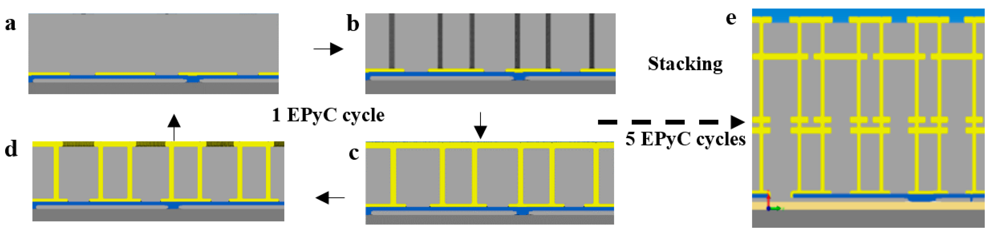
:1. Introduction
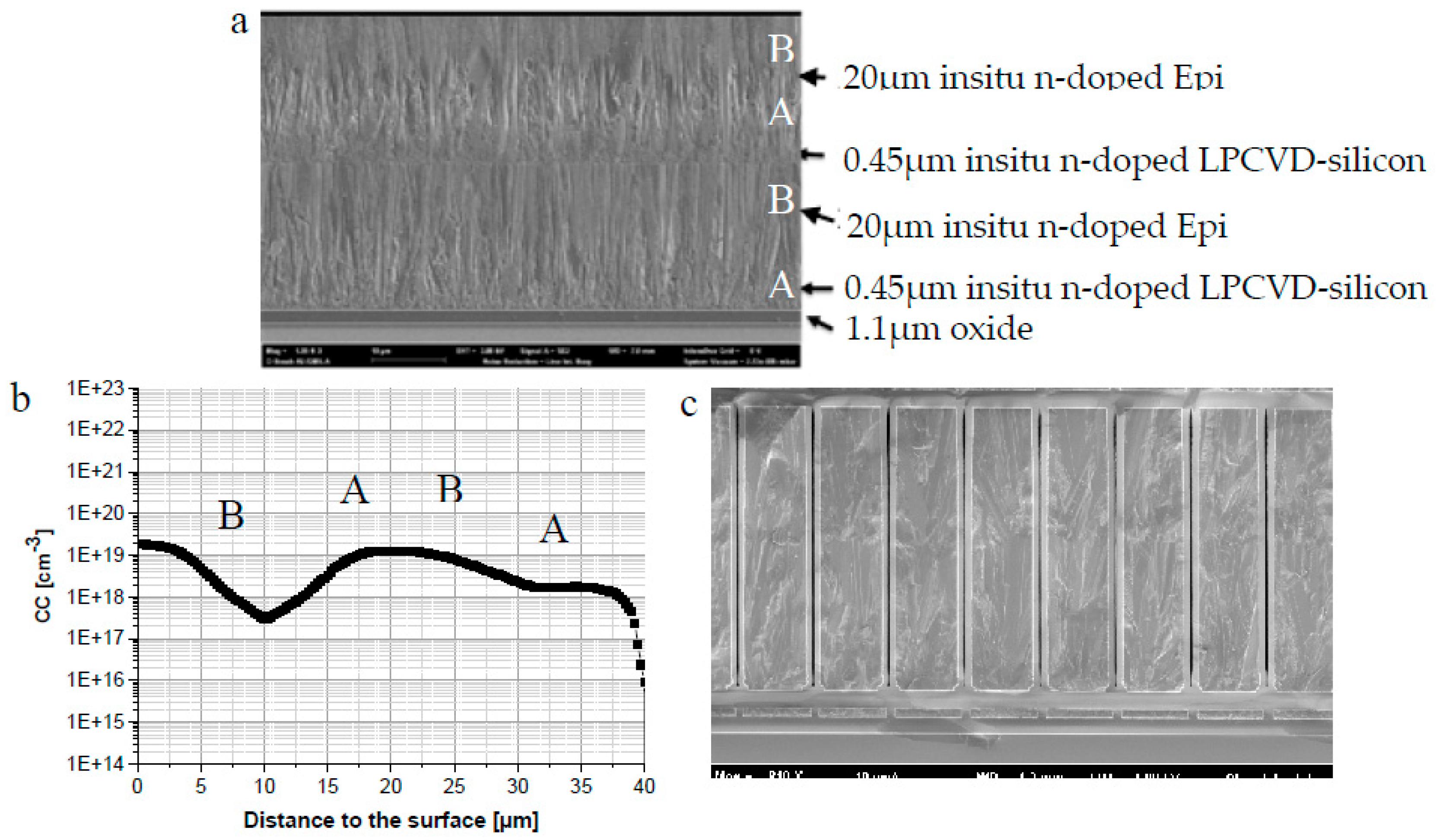
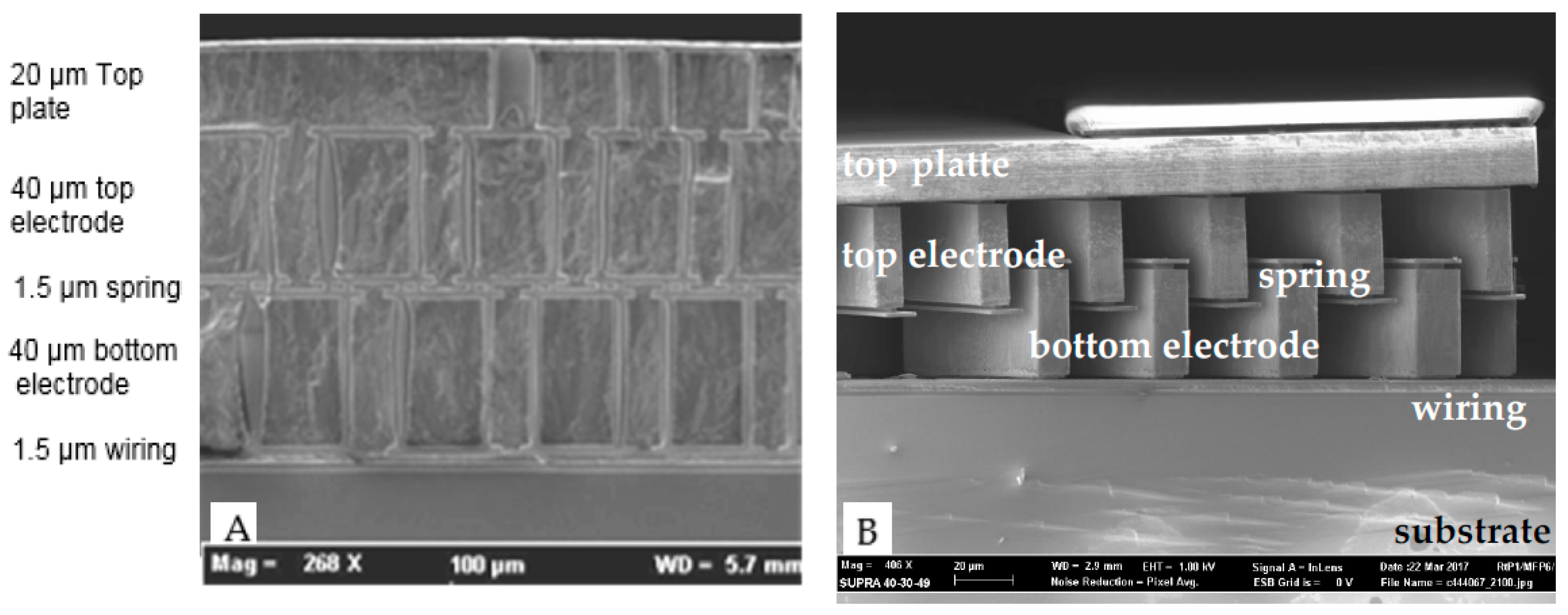
2. Vertical Comb Drive Realized by EPyC Process
3. Conclusions
Conflicts of Interest
References
- Development Laboratory Sandia National. Five Level Surface Micromachining Technology Design Manual, Version 3.2; MEMS Technologies; Development Laboratory Sandia National: Albuquerque, NM, USA, 2012. [Google Scholar]
- Mikia, N.; Zhangb, X.; Khannaa, R.; Ayo´nc, A.A.; Warda, D.; Spearinga, S.M. Multi-stack silicon-direct wafer bonding for 3D MEMS manufacturing. Sens. Actuators A 2003, 103, 194–201. [Google Scholar] [CrossRef]
- Metzger, L.; Fischer, F.; Mokwa, W. Polysilicon Sacrificial Layer Etching Using XeF2 for Silicon Acceleration Sensors with High Aspect Ratio. In Proceedings of the Eurosensors XVI, Copenhagen, Denmark, 27–30 August 2000. [Google Scholar]
- Breitschaedel, O.; Kaelberer, A.; Zielke, C.; Staffeld, P.B.; Artmann, H. Method for Manufacturing Microelectromechanical Structures in A Layer Sequence and a Corresponding Electronic Component Having a Microelectromechanical Structure. DE102015206996 A1, 20 October 2016. [Google Scholar]
- Louriki, L.; Staffeld, P.; Kaelberer, A.; Streiter, R.; Otto, T. 3D Printing in Silicon (EPyC-Process); Smart System Integration: Cork, Ireland, 2017. [Google Scholar]
- Louriki, L.; Staffeld, P.; Kaelberer, A.; Otto, T. Silicon sacrificial layer technology for the production of 3D MEMS (EPyC process). In Proceedings of the Eurosensors 2017, Paris, France, 3–6 September 2017. [Google Scholar]

Publisher’s Note: MDPI stays neutral with regard to jurisdictional claims in published maps and institutional affiliations. |
© 2017 by the authors. Licensee MDPI, Basel, Switzerland. This article is an open access article distributed under the terms and conditions of the Creative Commons Attribution (CC BY) license (https://creativecommons.org/licenses/by/4.0/).
Share and Cite
Louriki, L.; Staffeld, P.; Kaelberer, A.; Otto, T. Multilayer Micromechanics Process with Thick Functional Layers (EPyC40). Proceedings 2017, 1, 296. https://doi.org/10.3390/proceedings1040296
Louriki L, Staffeld P, Kaelberer A, Otto T. Multilayer Micromechanics Process with Thick Functional Layers (EPyC40). Proceedings. 2017; 1(4):296. https://doi.org/10.3390/proceedings1040296
Chicago/Turabian StyleLouriki, Latifa, Peter Staffeld, Arnd Kaelberer, and Thomas Otto. 2017. "Multilayer Micromechanics Process with Thick Functional Layers (EPyC40)" Proceedings 1, no. 4: 296. https://doi.org/10.3390/proceedings1040296