Proceeding Paper

Nanomechanical Traceable Metrology of Vertically Aligned Silicon and Germanium Nanowires by Nanoindentation

1
Institute of Semiconductor Technology (IHT), TU Braunschweig, 38106 Braunschweig, Germany
2
Laboratory for Emerging Nanometrology (LENA), 38106 Braunschweig, Germany
3
Department 5.1 Surface Metrology, Physikalisch-Technische Bundesanstalt (PTB), 38116 Braunschweig, Germany
4
Research Center for Physics, Indonesian Institute of Sciences (LIPI), 15314 Tangerang Selatan, Indonesia
*
Author to whom correspondence should be addressed.
Presented at the Eurosensors 2017 Conference, Paris, France, 3–6 September 2017.
Proceedings 2017, 1(4), 375; https://doi.org/10.3390/proceedings1040375
Published: 9 August 2017
(This article belongs to the Proceedings of Proceedings of Eurosensors 2017, Paris, France, 3–6 September 2017)

Abstract

:
Silicon and germanium pillar structures (i.e., micro- and nanowires) were fabricated by a top-down approach including nanoimprint lithography and cryogenic dry etching. Various etching parameters were tested to ensure a reliable fabrication process. The impression of nanomechanical properties of such 3-D structures were extracted experimentally by nanoindentation showing promising and comparative results to utilize such nanostructures as small force artefacts.

1. Introduction

Since the instrumented indentation technique has been introduced to determine hardness and elastic modulus of materials, this approach has been continuously becoming a leading standard in material science and engineering. Both scientific communities and industries have brought this method into a rapid development of commercial instrumentations and prototypes. Furthermore, advancement in measurement technique such as continuous stiffness measurement (CSM) in combination with precise displacement or force control provides more flexibility in terms of reliability on unloading curves [1]. Nevertheless, the most challenging task of such advanced technological improvements is to ensure traceability and reproducibility of the force measurements [2]. Refinements, testing, and applications on dissimilar materials with the aim of broader force range allow not only depth sensing measurements on very small and 2-D thin films structures [3], but also determination of 1-D nanostructure characteristics [4]. In this case, better understanding of anisotropic mechanical properties (e.g., the unloading curves) of various materials [5] and identification of nanoscale stress-strain characteristics [6] are important to ensure reliable integration of nanostructures within micro-/nanoelectromechanical systems (M/NEMS).

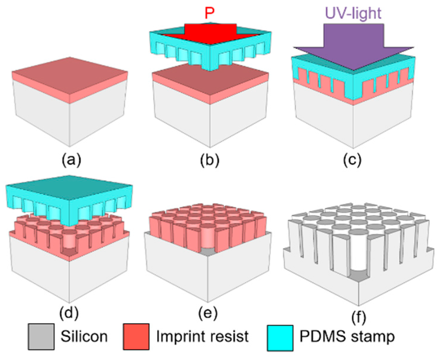
2. Fabrication of Vertical Nanowires

The fabrication steps of silicon micro- and nanostructures are shown in Figure 1. In this contribution, we utilized nanoimprint lithography (NIL) in order to avoid limitations showed by other etch mask preparation techniques, e.g., photolithography and colloidal lithography [7]. Initially, a 2-inch (100)-silicon wafer (SIEGERT Wafer GmbH, Aachen, Germany) was diced into smaller pieces of 15 mm × 15 mm substrate. Following this step, the substrate was dipped in buffered hydrofluoric acid and O2 plasma treatment was applied to remove the native oxide layer and residual surface contaminations, respectively. Afterwards, imprint resist (UVCur06, micro resist technology GmbH, Germany) was spin coated on the substrate and prebaked to remove excess solvent (Figure 1a). A soft PDMS stamp was created by replicating the Si master mold containing pillar structures. As a result, the PDMS stamp consists of hole structures, which were filled by the resist during the subsequent imprint step (Figure 1b). As soon as the pressure was evenly distributed and the stamp was self levelled, the resist was illuminated by UV-light (Figure 1c). After stamp detachment (Figure 1d), the desired patterns were transferred onto the resist, the residual resist layer was removed (Figure 1e) and the substrate was dry-etched at cryogenic temperature resulting in silicon 3-D structures (Figure 1f).
Full control of nanostructures fabrication was obtained by applying a sweep of etch parameters. We investigated several parameters (i.e., O2 percentage, temperature, and chamber pressure) during the inductively coupled plasma (ICP) reactive ion etching (RIE) at cryogenic temperature (Sentech Instrument GmbH, Berlin, Germany). We performed the experiments with the following initial recipe: an ICP Power of 150 W, a HF power of 10 W, SF6 and O2 flow rates of 60 and 6 sccm, respectively, and a pressure of 1 Pa. Etch processes were carried out, with only one parameter being modified throughout each experiment while the others were kept constant. As shown in Figure 2a–c, the change of O2 content within process gases has a significant impact on structure morphology. By using a lower flow rate of O2 (i.e., 3% of the total process gases) (Figure 2a), an isotropic etch profile with relatively low etch rate (i.e., 54 nm/min) was realized. Increasing the O2 flow to 9%, a deeper etch profile with improved anisotropy was realized owing to a better sidewall passivation and a higher etch rate of 132 nm/min was obtained (Figure 2b). Further increase of O2 content (i.e., 14%) leading to a thicker passivation layer [8] caused a reduction of the etch rate to 68 nm/min (Figure 2c). Utilizing the optimized O2 flow (i.e., 9%), we modified the process temperature ranging from −85 °C to −120 °C. Silicon cryogenic dry etching is known to be very sensitive to process temperature. At a temperature of −85 °C, an etching depth of around 2.4 μm was attained, while utilization of lower temperatures (i.e., −105 °C and −120 °C) caused not only crystal-plane-dependent etching, but also a reduction of the etch rate (Figure 2d–f). One can control the etch depth by controlling the chamber pressure, since at higher chamber pressure the kinetic energy of the ion flux is reduced [9]. As a result, a gradual reduction of etch rate (i.e., 188 nm/min, 132 nm/min, and 68 nm/min) was apparent at increasing chamber pressure (i.e., 0.1, 1.0, and 2.0 Pa) (Figure 2g–i). In contrast, Germanium wafer was etched by using only lower SF6 flux (i.e., 10 sccm) combined with moderate plasma density of 100 W at room temperature. In this case, an etch rate of ~200 nm/min was obtained.

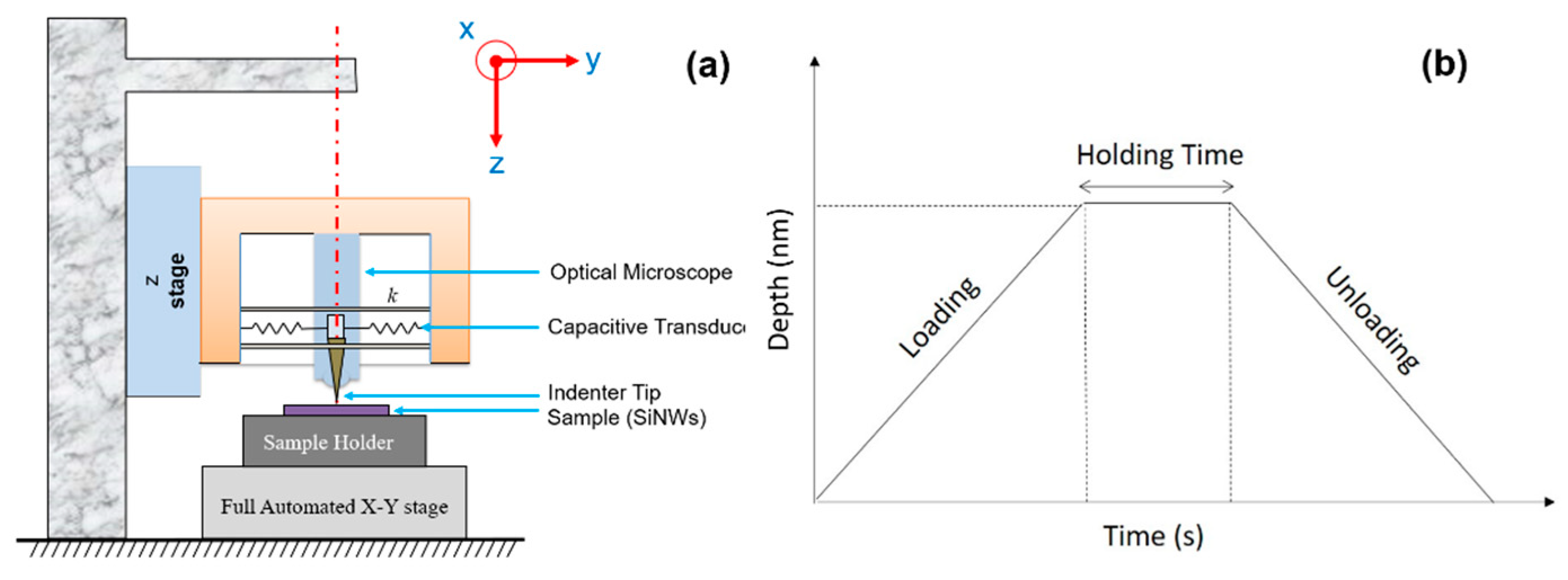
3. Nanomechanical Characterization

In this experiment, a Hysitron TI 950 TriboIndenter (Figure 3a) was used to perform nanoindentation tests on 3-D silicon structures and bulk silicon as a reference. This equipment has a maximum load force of 10 mN with a resolution of less than 30 nN, and a maximum indentation depth of 5 μm. Two approaches of load functions are available, i.e., the force- and the depth-controlled mechanisms. Following the theoretical explanation by Oliver and Pharr [10], the load function can be divided into three main parts, i.e., loading, holding, and unloading (Figure 3b).
The sample was mounted on the sample holder and indented by a Berkovich tip [11], where the indentation depth was measured by a capacitive sensor. The samples were indented by the tip in three steps, i.e., loading for 5 s, holding for 2 s, and unloading for 5 s. Each silicon pillar structure was indented in a scan size of 2 μm and each silicon bulk is indented in a scan area of 20 μm × 20 μm.

4. Results and Discussion

Based on the measurement procedure described above, indentation tests were performed both on bulk and 3-D structures of (100) and (111) silicon. Initially, the mechanical properties of bulk silicon (111) were determined by using the depth-controlled mode by applying different indentation depth from 40 to 130 nm. The stiffness values were differed depends on the indentation depth (e.g., material stiffnesses of around 106.13 μN/nm and 97.01 μN/nm were obtained for (111) and (100) silicon from indentation depth of 110 nm. With the same value of the indentation depth, we extracted more information related to anisotropic stress-strain behavior on 3-D materials by performing nanoindentation on silicon wires (i.e., (100) and (111) silicon) with a lateral size of ≥1000 nm and an aspect ratio of ~2 (Figure 4a,b). As a result, the extracted stiffness value of the (111) 3-D silicon structures (i.e., 58.64 ± 2.21 μN/nm) is more than two times lower than the value of the bulk material. The (111) silicon wires show a more rigid behavior than the (100) silicon wires with a stiffness of 32.84 ± 0.82 μN. Such differences between bulk and 3-D materials, as well as between 3-D materials of different orientations provide an open possibility for using 3-D silicon structures as test samples for nanoindentation calibration. Further comparison of nanoindentation tests with another elemental semiconductor (i.e., Germanium) will be performed.

Author Contributions

G.H., T.G., M.B., Z.L., and P.P. conceived and designed the experiments; G.H., Z.L., and P.P. performed the experiments; G.H., T.G., M.B., Z.L., and P.P. analyzed the data; Z.L., U.B., H.S.W., and E.P. contributed reagents/materials/analysis tools; G.H. wrote the paper.

Acknowledgments

The authors thank J. Breitfelder, M. Rühmann, A. Schmidt, and H. Yu for technical assistance. G. Hamdana and P. Puranto gratefully acknowledge support by Braunschweig International Graduate School of Metrology (B-IGSM) and funding by the German Research Foundation (DFG) under No. PE 885/3-1. P. Puranto thanks the Ministry of Research, Technology and Higher Education of the Republic of Indonesia (RISTEKDIKTI) for the PhD scholarship of RISET-Pro under No. 344/RISET-Pro/FGS/VIII/2016 and Indonesian-German Center for Nano and Quantum Technologies (IG-Nano) for the support.

Conflicts of Interest

The authors declare no conflict of interest.

References

  1. Oliver, W.C.; Pharr, G.M. Measurement of hardness and elastic modulus by instrumented indentation: Advances in understanding and refinements to methodology. J. Mater. Res. 2004, 19, 3–20. [Google Scholar] [CrossRef]
  2. Hamdana, G.; Bertke, M.; Doering, L.; Frank, T.; Brand, U.; Wasisto, H.S.; Peiner, E. Transferable Micromachined Piezoresistive Force Sensor with Integrated Double-Meander-Spring System. J. Sens. Sens. Syst. 2017, 6, 121–133. [Google Scholar] [CrossRef]
  3. Kim, M.S.; Pratt, J.R. SI traceability: Current status and future trends for forces below 10 microNewtons. Meas. J. Int. Meas. Confed. 2010, 43, 169–182. [Google Scholar] [CrossRef]
  4. Li, Z.; Gao, S.; Polenz, F.; Brand, U.; Koenders, L.; Peiner, E. Determination of the mechanical properties of nano-pillars using the nanoindentation technique. Nanotechnol. Precis. Eng. 2014, 3, 182–188. [Google Scholar]
  5. Datye, A.; Li, L.; Zhang, W.; Wei, Y.; Gao, Y.; Pharr, G.M. Extraction of Anisotropic Mechanical Properties From Nanoindentation of SiC-6H Single Crystals. J. Appl. Mech. 2016, 83, 91003. [Google Scholar] [CrossRef]
  6. Fujisawa, N.; Ogura, T.; Hirose, A. A Method for Studying the Nano-Scale Stress-Strain Response of a Material by Nanoindentation. Mater. Trans. 2016, 57, 1006–1009. [Google Scholar] [CrossRef]
  7. Hamdana, G.; Südkamp, T.; Descoins, M.; Mangelinck, D.; Caccamo, L.; Bertke, M.; Wasisto, H.S.; Bracht, H.; Peiner, E. Towards Fabrication of 3D Isotopically Modulated Vertical Silicon Nanowires in Selective Areas by Nanosphere Lithography. Microelectron. Eng. 2017, 179, 74–82. [Google Scholar] [CrossRef]
  8. Merzsch, S.; Steib, F.; Wasisto, H.S.; Stranz, A.; Hinze, P.; Weimann, T.; Peiner, E.; Waag, A. Production of vertical nanowire resonators by cryogenic-ICP-DRIE. Microsyst. Technol. 2014, 20, 759–767. [Google Scholar] [CrossRef]
  9. Miao, H.; Chen, L.; Mirzaeimoghri, M.; Kasica, R.; Wen, H. Cryogenic Etching of High Aspect Ratio 400-nm Pitch Silicon Gratings. J. Microelectromech. Syst. 2016, 25, 963–967. [Google Scholar] [CrossRef] [PubMed]
  10. Oliver, W.C.; Pharr, G.M. An improved technique for determining hardness and elastic modulus using load and displacement sensing indentation experiments. J. Mater. Res. 1992, 7, 1564–1583. [Google Scholar] [CrossRef]
  11. Berkovich, E.S. Three-faceted diamond pyramid for studying microhardness by indentation. Zavod. Lab. 1950, 13, 345–347. [Google Scholar]
Figure 1. Schematics of top-down fabrication of SiNWs (GeNWs) using NIL: wafer cleaning followed by spin coating of photo-curable resist on a silicon wafer (a). Resist templating (b). Curing (c). Stamp detachment and removal of residual resist layer (d,e). Pattern transfer by cryogenic dry etching (f).
Proceedings 01 00375 g001
Figure 2. Cross-sectional view of 3-D (100) silicon structures prepared by different etching parameters. Effects of O2 content (ac), process temperatures (df), and pressure (gi) on the fabricated features.
Proceedings 01 00375 g002
Figure 3. Nanoindentation setup (a) and load function during the indentation test (b).
Proceedings 01 00375 g003
Figure 4. Measured nanoindentation curves by applying a maximum displacement of 110 nm performed on silicon pillars with different crystal orientations (i.e., Si (100) (a) and Si (111) (b)) with an aspect ratio of 2 (D: diameter, AR: aspect ratio).
Proceedings 01 00375 g004
Publisher’s Note: MDPI stays neutral with regard to jurisdictional claims in published maps and institutional affiliations.

