Abstract
Chemical gas sensors are operated at elevated temperatures and the actual temperature has a tremendous influence on sensitivity and selectivity. From that perspective, precise temperature control over the chip is an absolute requirement. Next to a stable heating system, a controlled gas flow in the test box is required. The test gases should not cool down the sensor surface too much and not be heated up by the heater. To make the material integration easy and reduce the costs for sensor platforms, often rather large sensor devices are fabricated. We demonstrate that a combined approach of thermal analysis and computational fluid dynamics enables the co-design of gas flow path and heater to archive precise temperature conditions at the sensor material and in the surrounding test gas atmosphere.
1. Introduction
Electrochemical gas sensors have the chance to be one of the key elements for future environmental monitoring [1]. As they have to be operated at elevated temperatures up to 400 °C, one of the issues to solve is the energy consumption required for heating. The use of nanomaterials and very thin films [2] provides a large reduction in mass to be heated and enables at the same time short response time and high sensitivity. For temperature control, so called micro-hotplates [3] are used. These micro-hotplates have a very low mass and a small form factor, enabling fast temperature switching and integration into electronic systems. Both factors results in low power consumption. On the other hand, nanomaterials are often rather unstable at higher temperatures. To test for sensitive, selective and stable material combinations thus requires the test of various materials and corresponding process parameters. Fabrication of test samples and test of sensor effectivity is therefore a key element in material development and should be as cheap and fast as possible.
For research and development quite often rather large test chips are used, mainly because they are easy to handle and cheap to fabricate. They are also easy to functionalize by, e.g., drop, dip or spray coating.
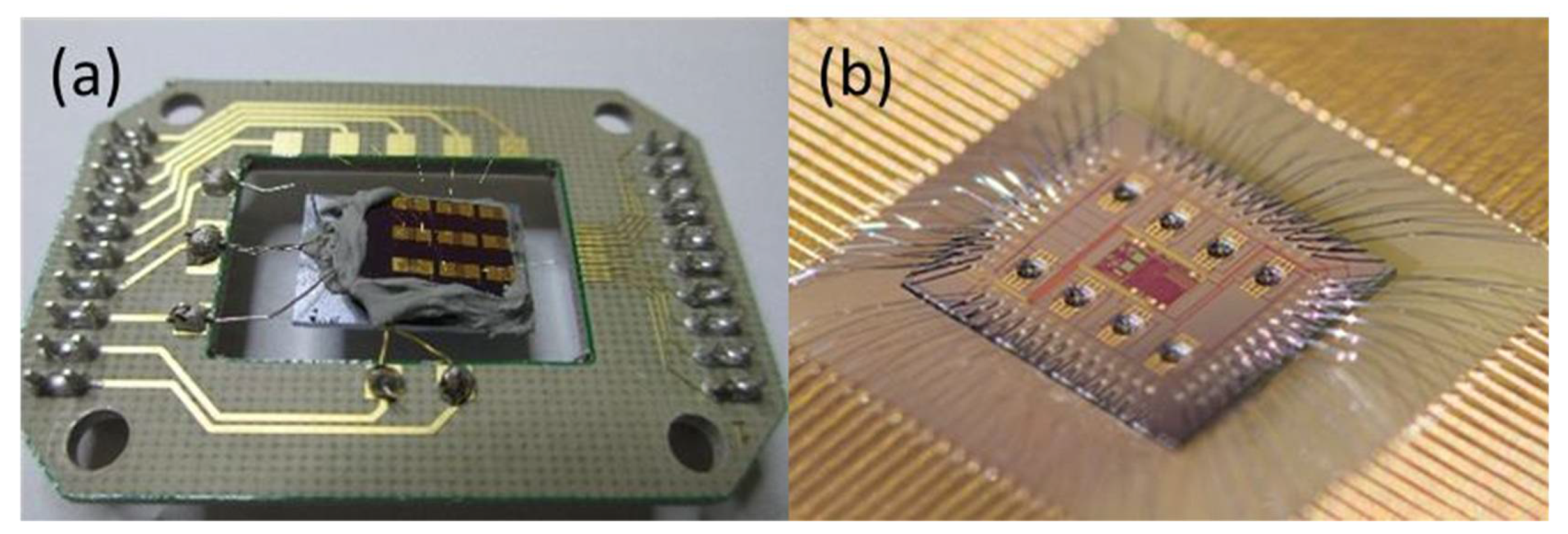
For testing sensitivity and selectivity, the chips are heated with external heaters. The Box I setup from MCL is shown in Figure 1a. In his case, the individual sensors have a dimension of about 1.5 × 4 mm2, the heated area is 10 × 20 mm2. This is contrast to the integrated micro hotplate arrays for multi gas sensors, as shown in Figure 1b. In this case, the heated area of an individual sensor is approximately 70 × 70 µm2.

Figure 1.
(a) Test chips on an external heater for MCL Box I setup. Wire bonds to a PCB electrically connect the sensors. They are mounted using thermo-conducive paste on a heating element with dimension of about 10 × 20 mm2. (b) CMOS integrated micro hotplate chip, heated area 70 × 70 µm2. This chip is also bonded by wire bonds to a PCB.
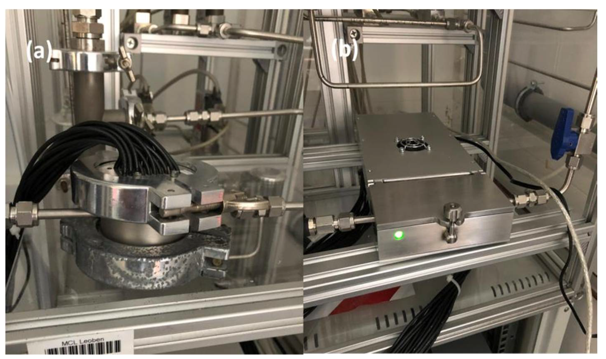
Another important aspect is the design of the test boxes, which should be adapted to the requirements of the sensors and their planned field of application. The gas inlets and the applied flow directly effects the final sensor behavior. Therefore, different types of gas boxes are used at MCL to enable application driven sensor material development, as shown in Figure 2. In both cases, the gas flow is in horizontal direction. Box I was designed for test chips with an external heater and external electronics control. The sensors are mounted with the heater on top and the sensor film down. The chamber has a volume of approximately 24 cm3. Box II, Figure 2b, has the electronics integrated in one platform and is specially designed for micro-hotplate sensors. The volume of the chamber is 100 cm3. This results in a turnover rate of gas per minute using of 42 in Box I and 10 in Box II respectively.
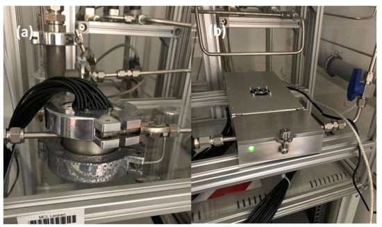
Figure 2.
(a) MCL Box I setup with the gasflow from the right to left. The cables lad to external data and control tools. (b) Box II with integrated electronics, special designed to work with CMOS gas sensors.
The gas flow over the sensors surface should not affect the basic characteristics of a sensing material like sensitivity and selectivity. On the other hand, temperature homogeneity over the sensing area and, when more than one sensors are mounted, over the heating plate is a key issue.
2. Method and Results
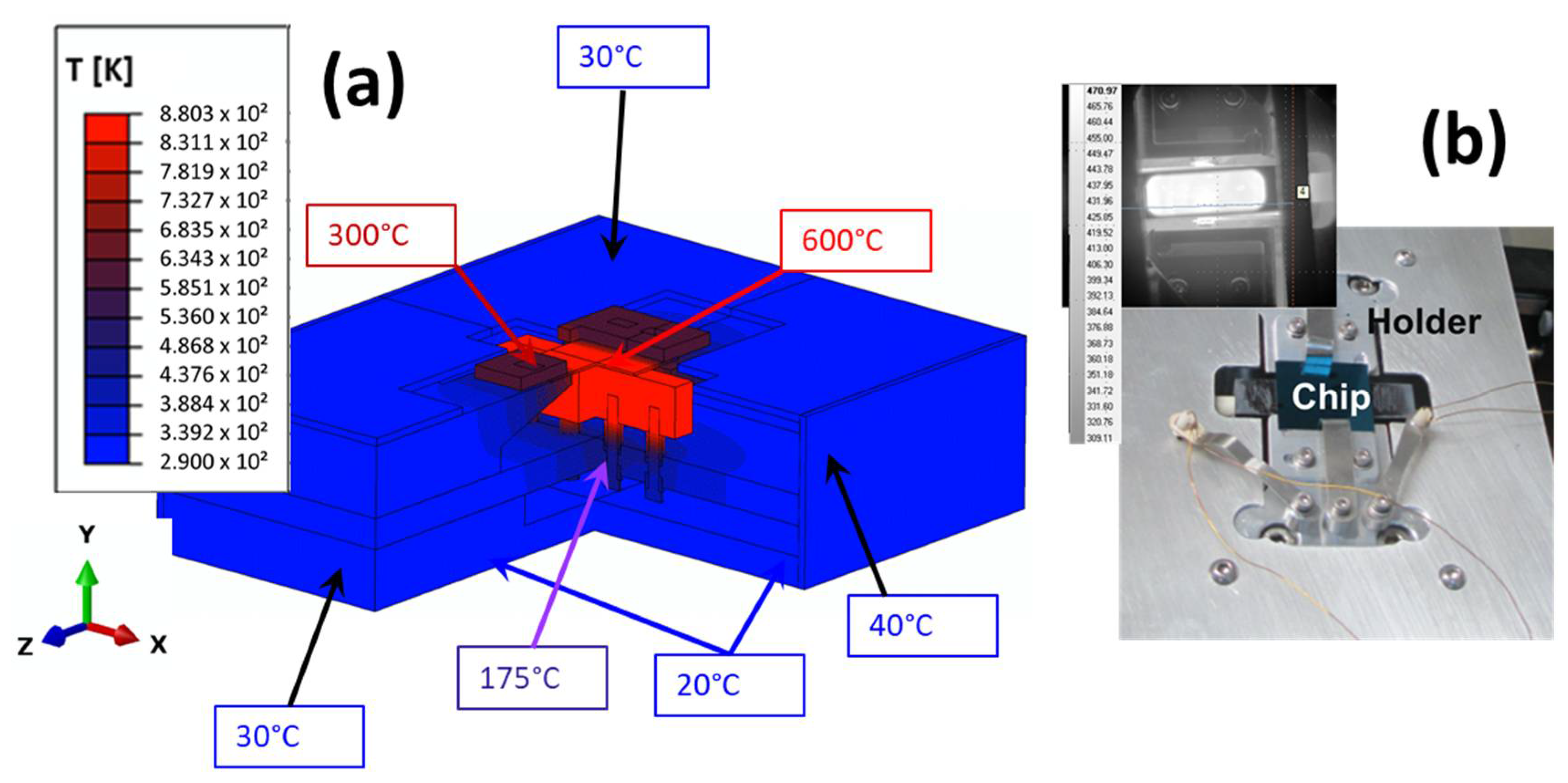
To archive homogenous temperature distribution at sensor surface, and to reduce the heating of the atmosphere above the sensor we used a combination of analysis and simulations in the design phase of the device. In a first step, a FE model of the first design is established. This allows simulate the heat dissipation inside the device and over the sensing area and a first materials selection for the buildup. This results in temperature profile estimations at the sensor and the surrounding and first test devices, as illustrated in Figure 3.
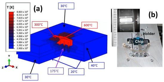
Figure 3.
(a) Buildup of the device in the FEM modeling program and FE calculation of the temperature distribution. (b) Image of the heater with a dummy chip and the thermography image of the heater in operation. Please note that Si is mainly transparent for IR and therefore the heater is imaged by thermography.
Thermocouples at different positions on the heater and the surrounding part enable to measure the local temperature. These values are used validation parameters for the simulations. Temperature and energy transport across the Si sensor towards the base material and the local temperature distribution of the hotplate is determined by thermography, shown in Figure 3b. These measurements are used to check and optimize the heat distribution of the heater. The next important step is the introduction of airflow along the sensor surface. When cold air is flowing over the hot sensor, the surface will be cooled, which will change sensor response. To study this influence, CFD simulations are coupled with the thermal simulation.
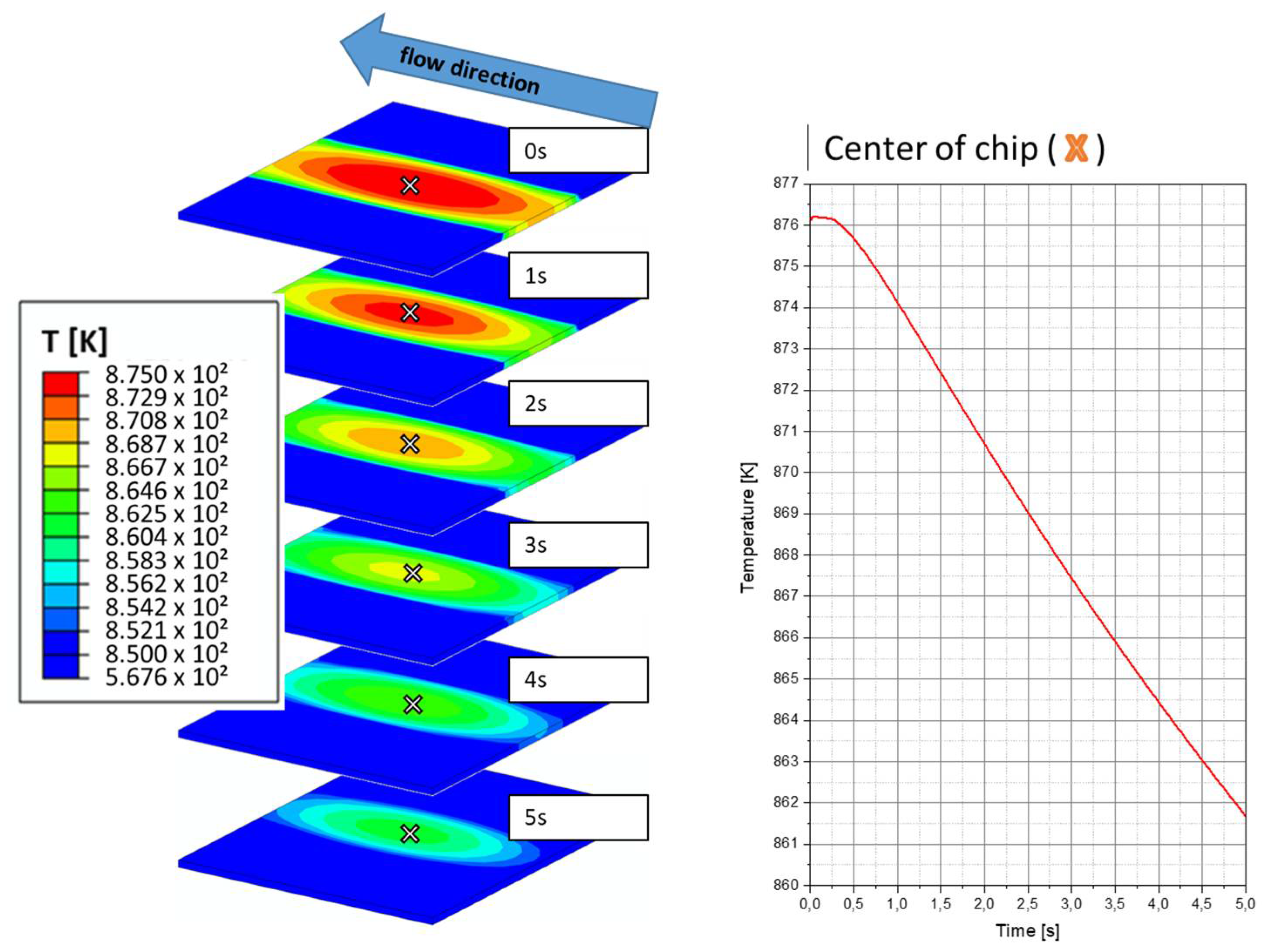
Without any airflow, the sensor chip surface will have the same temperature as the heating plate below. The temperature gradient over the chip is only a factor of thermal conductivity of Si and the thermal contact between chip and actively cooled surrounding. When an airflow is employed over the chip in the direction parallel to the heater, and the heater current is fixed, the sample chip surface is cooled down dramatically. We chose a flow of 5 m/s, which is a result from the overall flow of 1000 cm3/min from our gas mixture system and the chosen cross section of the chamber with a dimension of 15 × 20 mm2. Together with the lengths of 4 cm this correspond to a turnover rate for gas of 83. The results for a temperature simulation in the center of the chip is shown in Figure 4. Within 5 s of airflow, the temperature drops from approximately 400 °C to 384 °C and no steady state is reached in this time.
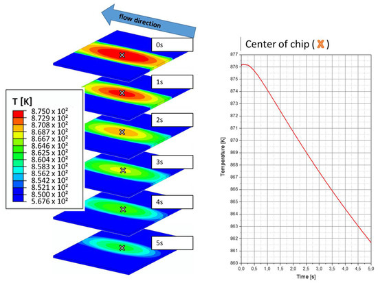
Figure 4.
Results from a combined CFD and heat transfer simulation. An arc indicates the flow direction. A gas flow of 5 m/s was chosen. In the center of the chip the temperature drops from 600 °C to 584 °C.
In the next step, an optimized design was developed and tested. This design includes reduction of amount of gas and optimizes the gas flow direction. Together with a control of heater the temperature homogeneity could be optimized.
3. Summary and Discussion
A method for the design of test equipment for electrochemical gas sensors is presented. This approach combines virtual and mechanical prototyping. Key aspects like temperature homogeneity on sensor surface and influence of flow geometry on cooling can be calculated using CFD calculations. Using the virtual methods, the amount of prototypes can be reduced and therefore costs can be saved.
Author Contributions
G.A.M. together with A.K. designed the study. G.A.M. was writing the first version of the contribution. C.K. did the construction work. M.K. established the simulations. All Authors read the contribution carefully and contributed to the content.
Acknowledgments
The financial aid of Austrian Funding Agency FFG within the “Production of Future” project FunkyNano (858637) is highly acknowledged.
Conflicts of Interest
The authors declare no conflict of interest. The founding sponsors had no role in the design of the study; in the collection, analyses, or interpretation of data; in the writing of the manuscript, and in the decision to publish the results.
References
- Yole Developent: “Gas Sensor Technology & Market”, February 2016. Available online: http://www.yole.fr (accessed on 16 November 2017).
- Tischner, A.; Maier, T.; Stepper, C.; Köck, A. Ultrathin SnO2 gas sensors fabricated by spray pyrolysis for the detection of humidity and carbon monoxide. Sens. Actuators B 2008, 134, 796–802. [Google Scholar] [CrossRef]
- Siegele, M.; Gamauf, C.; Nemecek, A.; Mutinati, G.C.; Steinhauer, S.; Kock, A.; Kraft, J.; Siezert, J.; Schrank, F. Optimized integrated micro-hotplates in CMOS technology (2013). In Proceedings of the 2013 IEEE 11th International New Circuits and Systems Conference, NEWCAS 2013, Paris, France, 16–19 June 2013. [Google Scholar] [CrossRef]
Publisher’s Note: MDPI stays neutral with regard to jurisdictional claims in published maps and institutional affiliations. |
© 2018 by the authors. Licensee MDPI, Basel, Switzerland. This article is an open access article distributed under the terms and conditions of the Creative Commons Attribution (CC BY) license (https://creativecommons.org/licenses/by/4.0/).

