Proceeding Paper

Polymer-CMOS Hybrid Neural Probes for Large-Scale Neuro-Electronic Interfacing †

KU Leuven, ESAT-MICAS, 3001 Leuven, Belgium
*
Author to whom correspondence should be addressed.
Presented at the Eurosensors 2018 Conference, Graz, Austria, 9–12 September 2018.
Proceedings 2018, 2(13), 1066; https://doi.org/10.3390/proceedings2131066
Published: 26 December 2018
(This article belongs to the Proceedings of EUROSENSORS 2018)

Abstract

:
Achieving a stable, long-term connection with millions of neurons within living organisms remains one of the dreams of neuroscience. Silicon shank based probes lead the field in terms of pure channel count. On the other hand, polymer neural probes offer superior biocompatibility, ruggedness and lower cost. This work tries to merge these technologies while exploring new electronic and interconnect design methods, ultimately yielding a prototype of a polymer-CMOS hybrid neural probe with a gold bump interconnect along with an electronic design based on bipolar transistor input devices, pseudo-capacitive AC coupling and in-pixel digitization.

1. Introduction

Achieving a long-term, high-bandwidth link between electronics and complex nervous systems remains one of great challenges of the today’s neuroscience. Recent years have yielded a renewed interest in this topic thanks to decreasing cost and increased availability of microfabrication and custom CMOS integrated circuit design. Ref. [1] represents one of most advanced solutions to date, consisting of a silicon shank neural probe co-integrated with a CMOS front-end in a single monolithic design. While attractive due to ease of fabrication, such designs are unsuitable for long-term use due poor mechanical and chemical biocompatibility. Furthermore, these devices are fragile and cannot be easily adapted towards other form factors, such as peripheral nerve or cortical surface electrodes.
The authors of this paper, among many others, have long recognized these problems which prompted research of flexible neural probes based on polymers which would offer far better mechanical matching with the tissue while being very inert and durable. Despite a plethora of research [2,3], these electrodes were so far limited to a small channel counts—usually less than 100. Typically, commercial off-the-shelf (COTS) connectors and cables are used to route the signals toward the external circuitry. Further scaling necessitates a much closer co-integration with an active integrated circuit that would house neural amplifiers, stimulators, and A/D conversion with a communication link multiplexed over a relatively small number of wires. This “hybrid” neural interface would combine the best of both worlds, merging the long-term biocompatibility of flexible probes with high density of monolithic designs. Such a close integration demands a high density interconnection between flexible neural probes and CMOS integrated circuits, which is highly reminiscent to interconnects used with multi-die image sensors, where a photodetector die is typically flip-chip bonded onto a CMOS readout integrated circuit (ROIC).
The goal of this work is to derive all the required knowhow in electrode, interconnect and IC design, as well as better understanding of scaling laws (akin to “Moore’s law”) that will govern the future evolution of neuro-electronic interfaces.

2. Materials and Methods

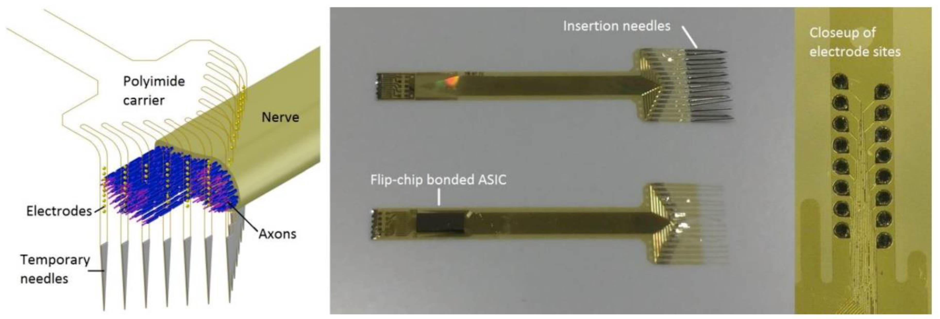
2.1. Electrode, Interconnect and Insertion Structure Fabrication

256-channel polyimide-based neural probes (Figure 1) aimed at interfacing rat sciatic nerves were fabricated using a process similar to [2] except a layer of gold (~150 nm) was used on the top of 50 nm platinum to facilitate electroplating. Iridium oxide (200 nm) was sputtered onto electrode sites to lower the AC impedance. Gold bumps were electroplated using a maskless method in Semiplate Au 100 solution (Microchemicals GmbH, Ulm, Germany) for 100 min yielding ~15 μm bump height. Contacting was achieved indirectly using conductive nickel ink on the electrode sites. A Fineplacer Lambda bonder was used at following settings: 2 kg force, temperature 180 °C, ultrasound power: 20 W, ultrasound time: 300 ms, number of bumps: 256.

2.2. Electronic Design

Despite the numerous neural amplifier related publications in the recent years, as summarized in [4], few authors consider their large-scale integration into image-sensor style arrays. Capacitive feedback operational amplifiers remain among most popular designs. However, they are notorious for a high area consumption dominated by AC coupling capacitors and the input transistors.
The chip design presented in this work (Figure 2) attempts to tackle these drawbacks in several ways. Its design emulates a single image-sensor row with 256 “pixels” in which the photodiode input is replaced by simple near-threshold inverter amplifier similar to solution proposed in [4], except the input is DC-coupled and an auxiliary input is provided for offset compensation signal which is broadcast from an external DAC. Outputs are multiplexed using inverter buffer amplifiers, which are switched into virtual ground. In overall, each pixel contains only 10 transistors showing a great miniaturization potential. The chip was fabricated using ON Semi 350 nm process and tested using simple cockroach cell preparations.
Furthermore, several new circuit techniques were tested with COTS components, such as direct AC coupling via electrode pseudo-capacitance, use of bipolar junction transistor (BJT) low noise amplifiers and in-pixel digitization using delta-sigma modulators.

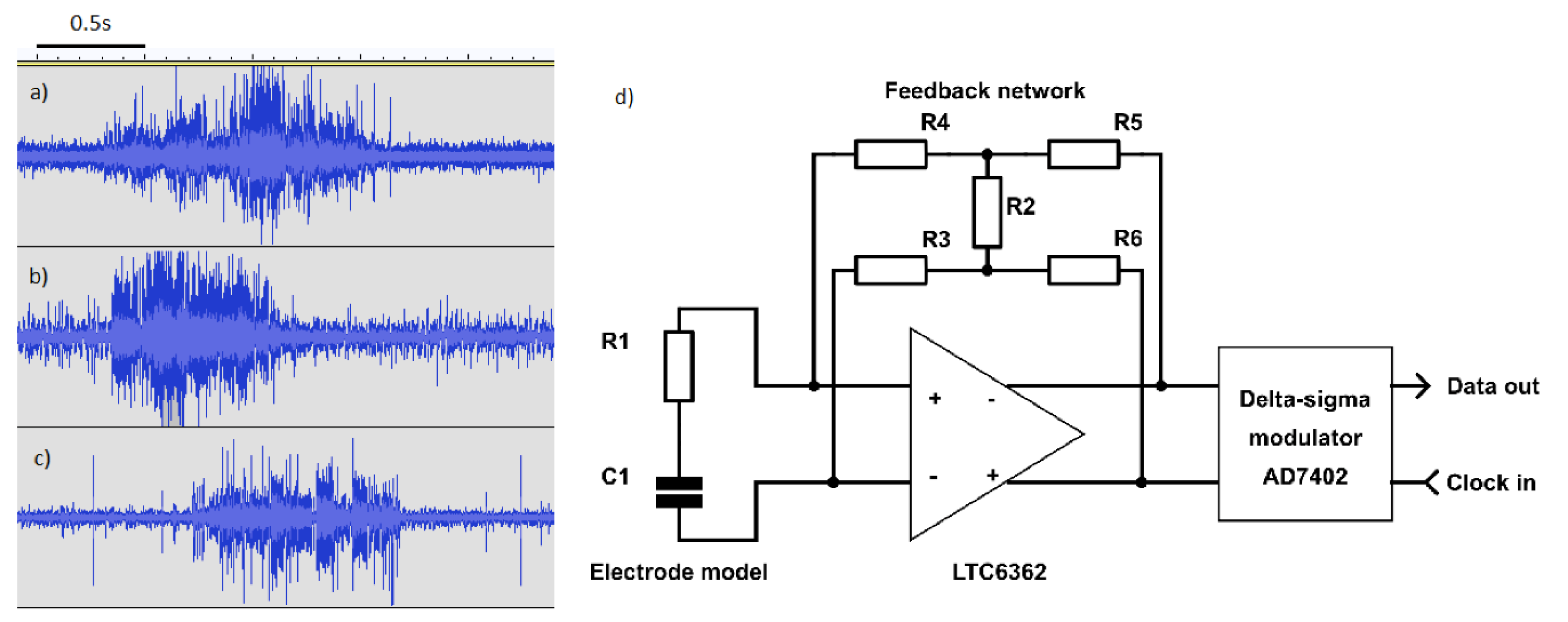
2.3. Electrophysiological Testing

Ventral nerve cords and individual legs of Maderia cockroaches (Rhypharobia maderae) were used to test the neural probes and electronics. To evaluate the recording amplifiers, legs were penetrated through tibia with Ag/AgCl wires 1–2 mm apart, and action potentials evoked by mechanical stimulation of tactile spines using a cotton swab.

3. Results and Discussion

3.1. Hybrid Assembly

Electroplated gold bumps showed good uniformity despite the indirect contacting method which results in several kΩ of additional series resistance per bump. Successful bonding was confirmed by a shear test (Figure 3, middle, right), upon which the bumps are transferred to the chip, as seen in the Figure 3, right. One un-plated site, caused by a broken trace, is shown for reference. However, upon inspection from the back, it can be seen that the base metal is deformed and delaminated, with very little adhesion left. An attempt was made to improve this with a “rivet” shaped bump (Figure 3, left) that penetrates all the way through the substrate, yielding better mechanical properties and easier handling. Nevertheless, with an achieved pitch of 60 μm, to the knowledge of the authors, this is the most dense polymer neural probe interconnect achieved to date.

3.2. Electronic Testing and Measurements

The first fabricated chip was successfully tested using cockroach leg preparations in both static (single amplifier selected) and scanning regime with sample recordings shown on Figure 4a,b. However, extrinsic noise remains high due to poor common mode signal rejection of single-ended amplifiers, along with a tendency to down-convert high-frequency interference.
On the other hand, the fully differential digital pixel prototype has demonstrated near-theoretical noise performance, high common mode rejection and ease of scaling due to digital output and lack of chip-wide feedback systems, making it a much better candidate for future large-scale designs. Authors of [5] demonstrate designs of very small delta-sigma modulators, suitable for future CMOS integration.

4. Conclusion and Future Research

Electroplated gold micro-bumps represent a good candidate for a high-density interconnect between CMOS integrated circuits and polyimide-based neural probes. Future work will explore various other interconnect options, such as micro-soldering and even incorporation of chip dies into microelectrode fabrication flow and direct contacting using a lift-off process. In the aspect of electronic design, a self-contained “digital pixel” topology shown in Figure 4 possesses numerous advantages over analog-multiplexed methods and is under research for future CMOS integration.

Author Contributions

M.B. and F.C. conceived, designed and performed the experiments; M.B. analyzed the data; R.P. contributed reagents/materials/analysis tools; M.B. and R.P. wrote the paper.

Acknowledgments

This work is funded by the ERC under the EU’s Seventh Framework Program (FP7/2007-2013)/ERC grant agreement n° 340931, and was sponsored by the KULeuven IDO program, project on electrical brain stimulation IDO/12/024.

Conflicts of Interest

The authors declare no conflict of interest.

References

  1. Lopez, C.M.; Putzeys, J.; Raducanu, B.C.; Ballini, M.; Wang, S.; Andrei, A.; Rochus, V.; Vandebriel, R.; Severi, S.; Van Hoof, C.; et al. A Neural Probe with with Up to 966 Electrodes and Up to 384 Configurable Channels in 0.13μm SOI CMOS. IEEE Trans. Biomed. Circ. Syst. 2017, 11, 510–522. [Google Scholar] [CrossRef] [PubMed]
  2. Ceyssens, F.; Puers, R. Insulation lifetime improvement of polyimide thin film neural implants. J. Neural Eng. 2015, 12, 054001. [Google Scholar] [CrossRef] [PubMed]
  3. Xiang, Z.; Yen, S.C.; Xue, N.; Sun, T.; Tsang, W.M.; Zhang, S.; Liao, L.D.; Thakor, N.V.; Lee, C. Ultra-thin flexible polyimide neural probe embedded in a dissolvable maltose-coated microneedle. J. Micromech. Microeng. 2014, 24, 065015. [Google Scholar] [CrossRef]
  4. Bharucha, E.; Sepehrian, H.; Gosselin, B. A survey of neural front end amplifiers and their requirements toward practical neural interfaces. J. Low Power Electron. Appl. 2014, 4, 268–291. [Google Scholar] [CrossRef]
  5. Mahmoodi, A.; Joseph, D. Pixel-level delta-sigma ADC with optimized area and power for vertically-integrated image sensors. In Proceedings of the 2008 51st Midwest Symposium on Circuits and Systems, Knoxville, TN, USA, 10–13 August 2008. [Google Scholar]
Figure 1. Neural probes for rat sciatic nerves. Left: concept, right: fabricated samples.
Proceedings 02 01066 g001
Figure 2. (Left) Block diagram of the recording system; (Right) Pixel-level schematic.
Proceedings 02 01066 g002
Figure 3. (Left) Au bumps pre- and post-bonding. (Middle) shear test. (Right) sheared bump close-up.
Proceedings 02 01066 g003
Figure 4. Neural recording from cockroach mechanoreceptors using (a) static, single ASIC channel; (b) dynamic (scanning 256 channels), (c) recording via COTS circuit shown at (d).
Proceedings 02 01066 g004
Publisher’s Note: MDPI stays neutral with regard to jurisdictional claims in published maps and institutional affiliations.

