Proceeding Paper

Silicon-On-Nothing Micro-Pirani Gauge for Interior-Pressure Measurement †

by
Andrey Kravchenko
1,*,
Vladislav Komenko
1 and
Wolf-Joachim Fischer
2
1
Infineon Technologies Dresden GmbH, 01099 Dresden, Germany
2
Institute of Semiconductors and Microsystems, TU Dresden, 01187 Dresden, Germany
*
Author to whom correspondence should be addressed.
Presented at the Eurosensors 2018 Conference, Graz, Austria, 9–12 September 2018.
Proceedings 2018, 2(13), 1079; https://doi.org/10.3390/proceedings2131079
Published: 20 November 2018
(This article belongs to the Proceedings of EUROSENSORS 2018)

Abstract

:
In the current work, we present a compact and cost effective Pirani gauge based on Silicon-On-Nothing (SON) technology. The proposed design uses an innovative approach of etching the sensing element directly in a crystalline silicon membrane. Such configuration allows pressure dependent heat losses to act on the substrate not only through the bottom cavity and trenches but also via the top cavity on the lid, which is formed by means of a sacrificial layer. By ensuring process compatibility with other SON-based MEMS, the proposed device can be used as a tool for cavity pressure monitoring and product support over the whole life cycle of MEMS: ranging from fabrication to calibration during field tests. Performance of the device is investigated based on numerical simulations and measurements. Furthermore, work includes a discussion of the fabrication process along with an additional cavity pressure characterization.

1. Introduction

Pirani gauge is a widely-spread measurement tool commonly used in low pressure setups. In such class of devices sensing is performed by monitoring the amount of energy required to heat up the filament. Structures are designed to maximize the pressure dependent losses through the air. Any energy loss through the solid materials is on the contrary, reduced. Pressure-sensitive operation range then lies between the continuum flow regime boundary on one side and constant losses on the other. Although operation principles are well-known and numerous variants are available in the market, integrated and CMOS compatible solutions are still a topic of research. Most manufacturing approaches rely on either polysilicon or metals as the filament material. In combination with more complex processing, compatibility with other devices might be difficult to achieve. However, the use of crystalline silicon should result in better performance, reliability and cost reduction. The focus of this work is a compact SON-based solution capable of integration alongside other MEMS devices as well as compatible with standard CMOS process.

2. Materials and Methods

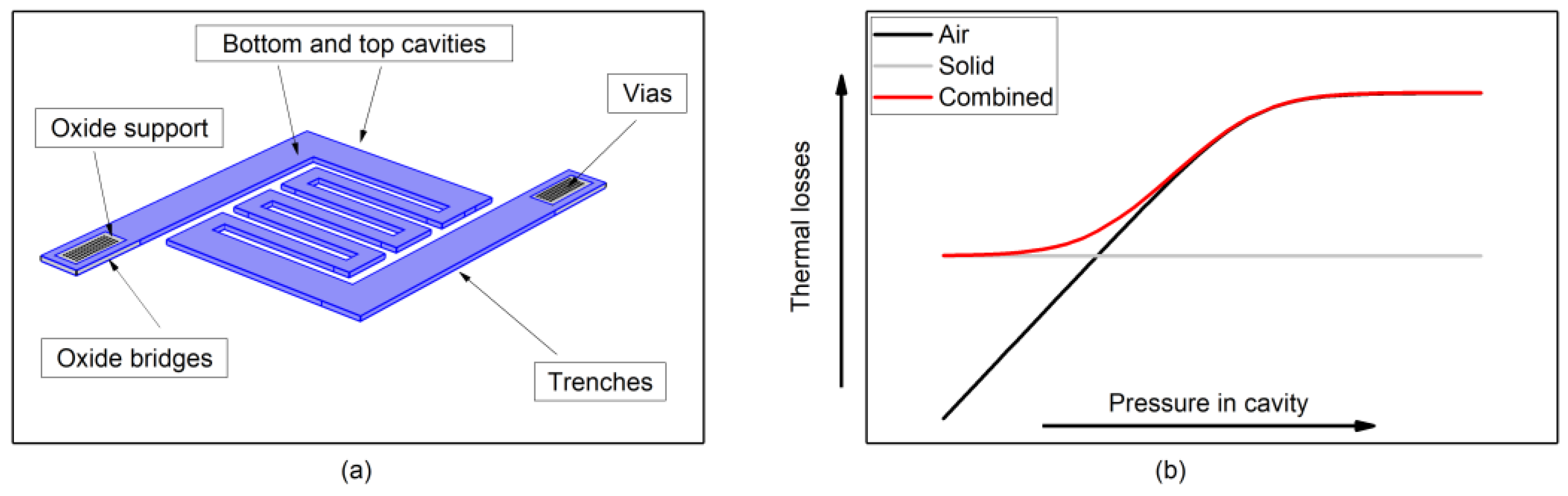
2.1. Geometry and Materials
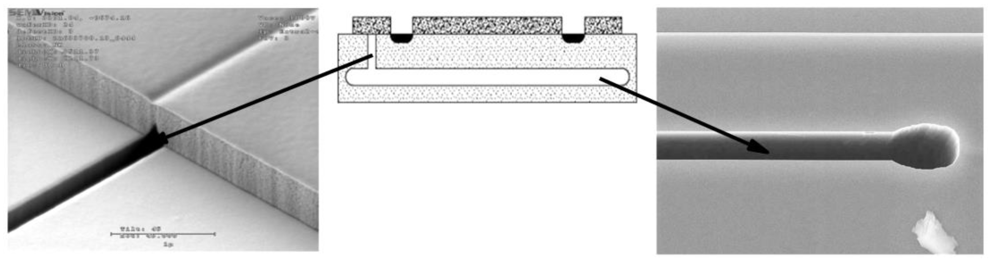
General shape of the device can be seen in Figure 1a. It comprises of a meander shaped filament supported by cantilevers on the sides. Bottom and top cavities formed by means of the SON process and a sacrificial layer respectively allow mechanical and electrical decoupling from the bulk with only an oxide bridge connection at the base of the cantilevers in the area of the contacts.
As shown in Figure 1b, losses can be divided into solid, that include all the mechanical connections (metal contacts, oxide pylons and silicon filament) and eventually define the lower boundary of the sensitivity range, and fluid losses where pressure plays a critical role. Dependent on the Knudsen number given by the ratio of the mean free path to the travelling distance between the walls, three operation regimes are defined: continuum regime, transitional and free molecular flow. For higher values of Knudsen number, properties of air saturate. This is explained by a large molecule interaction count. Once the pressure is lowered, the regime changes through transitional to free molecular flow, where molecules travel over the target distance with little interaction. In this case the heat transfer depends strongly on the pressure [1]. All the thermal losses were modelled as either boundaries with heat transfer coefficient assigned to them, as in case of air, or as solid materials with temperature dependent properties included [2]. Electrical model, however, is mostly limited to the silicon heater. Based on the implant type, appropriate mobility model was chosen and included into the total conductivity calculation.

2.2. Manufactering

Fabrication follows the standard SON process. While the bottom cavity is formed, a blanket implant is used to define electrical properties of the membrane. This is followed by the 1st deep trench etch to partially cut out what will later be the filament of the gauge. Further processing proceeds with a sacrificial layer deposition for top cavity structuring. Results to this step are available in Figure 2. One can see how the trenches are opened when the sacrificial layer is patterned.
To form the lid a CVD-oxide was selected. At this stage the supporting oxide bridges at the cantilever bases as well as the pylons for vias are formed. Next step mechanically decouples the filament from the substrate by means of a 2nd deep silicon etch step with a mask complementary to the one used for the 1st trench. All openings are further sealed with another oxide deposition. A two trench approach allows easy integration of suspended structures with a sealing. During metallization in back-end processing tungsten with a TiN/Ti liner was used for filling the vias; aluminum was the material chose for interconnects. Final treatment includes an oxide etch to enable access to the sacrificial layer and a consecutive isotropic plasma strip to release the structure. At this stage the filament is suspended only on the cantilever ends. One wafer was taken to perform the open measurements such as reliability and pressure sensing characterization. The other one was additionally passed through an oxide sealing and is later used to investigate the outgassing effects.

3. Results

3.1. Open Cavity Characterization

Previously discussed geometry and boundary condition arrangement was investigated by means of FEM analysis to assess performance at various pressure levels. As can be observed in Figure 3a, with increasing power the filament starts to heat, what is indicated by the increase in electrical resistance. At some point the temperature exceeds a certain value and intrinsic conductivity start dominating leading to a resistance drop. Manufactured devices were characterized to confirm expectations based on numerical analysis. The results are available in Figure 3b. Comparing with the associated plots obtained by modelling one can immediately observe a similarity in the curve profiles.
In pirani gauges pressure sensing is performed by monitoring the amount of input power that has to be spent in order to achieve a reference temperature. Since the filament heating is linked to the electrical conductivity, two reference resistance values were chosen. First one corresponds to the maximal resistance; second one is defined as 250 Ohm change from the initial cool state. Rearranging the data and plotting the corresponding values leads to a relation show in Figure 4.
It can be clearly identified that the structure loses its sensitivity for values below 10 mbar. At that moment the losses are dominated by the thermal conductivity of the solid materials. The upper limit is expected to be 10 bar. Above that pressure the losses are still dominated by the air, but the continuum regime limits the sensitivity.

3.2. Sealed Cavity Characterization

Knowing how the structure behaves at various pressures, it is now possible to perform investigation of the closed structures, where operating conditions are unknown. In CVD films, once the ambient temperature approaches the one of deposition, out-gassing takes place thus increasing the pressure inside of the cavity. It is expected that the pressure is set while the structure was exposed to highest temperature. Lowering it afterwards should not impose any additional changes.
During the experiment input power was first gradually increased to achieve greater temperatures in the filament and enforce out-gassing. Ramp down sequence was introduced to assess the possibility of pressure to stabilize at a constant value. This is critical for operation of IR-Emitters, where thermal stability and reproducibility has to be ensured. Since the structure was initially characterized at two conditions: first at peak resistance and second at the 250 Ohm change, two separate assessments can be performed. Investigation with the first approach, presented in Figure 5a, indicates that the minimal power of 60 mW has to be applied in order to acquire the first measurement point. Unfortunately, the curve dynamic points out that the out-gassing started even before the first point could be extracted. As opposed to the first approach, the second curve enables pressure calculation at lower temperatures. As can be seen in the corresponding Figure 5b, at lower input powers the pressure saturates at 65 mbar and only starts increasing once 40 mW are applied. It is clear why the previous measurement attempt with the peaks did not succeed, the minimal power to get the first measure point was at 60 mbar, this is already above the threshold where out-gassing starts. Finally, during power ramp down both measurements saturate at 80–85 mbar reached at 180 mW of input power.

4. Discussion

Within the current work we presented an integrated pirani gauge with a crystalline silicon filament. Device was fabricated based on the SON technology and was proven to operate in the range between 10 mbar and 1 bar, with a simulated sensitivity range extending to 10 bar. Out-gassing characterization was performed at 2 different reference temperatures with a minimum required input power set as 60 mW and 40 mW depending on approach. Both investigations lead to comparable results with initial cavity pressure being 65 mbar and increasing to 85 mbar after 180 mW was applied. Presented structure can be used as a stand-alone device or as an in-line process characterization and monitoring tool. In the second case devices can be efficiently placed in the dicing areas with no additional costs for manufacturing.

Author Contributions

A.K. and V.K. contributed to concept development and paper writing. A.K. performed the numerical modeling and device characterization while V.K. worked on processing and fabrication topics. W.-J.F. supported and guided the work.

Acknowledgments

Technical and resource support of Infineon Dresden GmbH is gratefully acknowledged.

Conflicts of Interest

The authors declare no conflict of interest.

References

  1. Cheung, K. Modelling a MEMS Thermal Conductivity Pressure Sensor for the Evaluation of Glass Frit Vacuum package. J. Nano-to-Macro Energy Transp. 2004. December. Available online: http://mit.sustech.edu/NR/rdonlyres/Mechanical-Engineering/2-57Fall-2004/0F5D19BC-5AE0-4B99-BA3A-661D9F0F6E9C/0/cheung_sensor.pdf.
  2. Reggiani, S.; Valdinoci, M.; Colalongo, L.; Rudan, M.; Baccarani, G.; Stricker, A.D.; Illien, F.; Felber, N.; Fichtner, W.; Zullino, L. Electron and hole mobility in silicon at large operation Temperatures. I. Bulk mobility. AIEEE Trans. Electron Devices 2002, 49, 490–499. [Google Scholar] [CrossRef]
Figure 1. (a) Geometry and thermal loss sources, (b) Pressure dependency of thermal losses.
Proceedings 02 01079 g001
Figure 2. Sacrificial layer over deep trench and SON membrane.
Proceedings 02 01079 g002
Figure 3. (a) Modelled and (b) measured gauge heating response at different pressured.
Proceedings 02 01079 g003
Figure 4. Modelled and measured gauge response at selected conditions.
Proceedings 02 01079 g004
Figure 5. Estimated pressure at (a) peak resistance and (b) 250 Ohm change.
Proceedings 02 01079 g005
Publisher’s Note: MDPI stays neutral with regard to jurisdictional claims in published maps and institutional affiliations.

