Abstract
One of the main difficulties for a global implantation of the Internet of Things (IoT) is the energy dependence of the nodes, limited by the battery’s lifetime. Energy harvesting seems to be a promising solution to provide energy autonomy to IoT nodes. Power management circuits are needed to collect and store the charges scavenged form the ambient sources. In addition, this circuit needs to adapt the output voltage to power the wireless sensor node. Because of the typical heterogeneity of the system, the cost and difficulties associated to the encapsulation of the CMOS chip and the energy harvester can be important. They could be reduced by using a monolithic integration of both parts in a single chip or package. In this work, we propose a fully monolithically integrated system comprised by a power management circuit, a piezoelectric microgenerator and a storage capacitor. With this solution, which combines MEMS and CMOS technologies, we pave the way to the future development of autonomous smart dust.
Keywords:
IoT; MEMS; energy harvesting; monolithic integration; piezoelectric; CMOS; charge pump; self-powered; AlN 1. Introduction
The interest in Internet of Things (IoT) is increasing exponentially in the last years [1]. One of the main difficulties for a universal implantation of the IoT concept is the energy dependence of the nodes, which is limited by the battery’s lifetime. An alternative to avoid this limitation is the harvesting of ambient energy to power these devices, such as vibrations, heat or light. In most cases, the available ambient energy is limited. Further, power management circuits for energy harvesting need to collect the generated charges and adapt the output to the operation voltage of the nodes of a wireless sensor network (WSN). The subsequent cost of encapsulating the microgenerator together with the power management circuit could be reduced if they are integrated in a single chip with compatible fabrication technologies [2]. Our goal is to obtain a monolithic system comprised by the integrated converter circuit and the piezoelectric generator device, combining MEMS and CMOS technologies.
2. Piezoelectric MEMS Energy Harvester
Our proposed vibration-driven energy harvesters, shown in the Figure 1, consist of MEMS cantilever-like structures [3] with piezoelectric layers of AIN deposited by RF sputtering. The fabrication process for these devices is based on SOI wafers (Silicon: 15 µm—SiO2: 1 µm—Silicon: 500 µm) etched by Deep Reactive Ion Etching (DRIE) and the deposition of metals and AIN [4]. In order to increase the bandwidth of these types of MEMS resonators, non-linear resonances will be exploited.
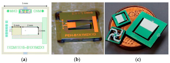
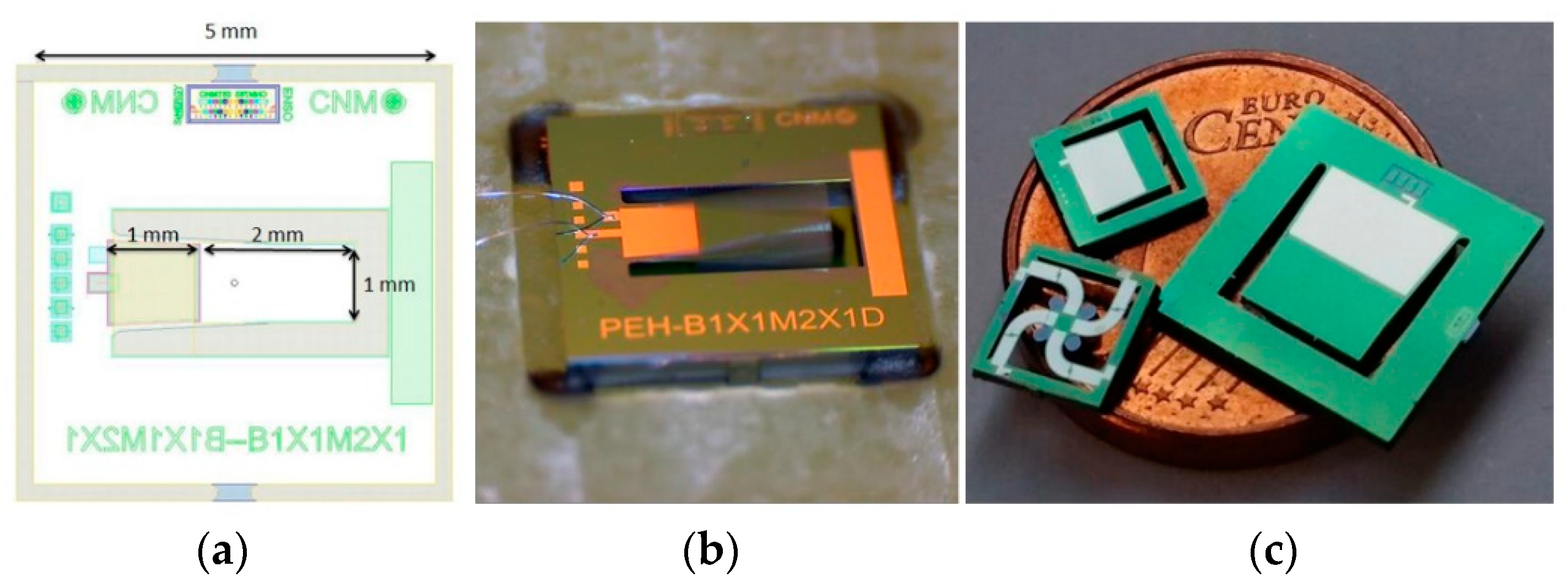
Figure 1.
(a) Diagram and size of a piezoelectric microgenerator (5 mm × 5 mm × 0.516 mm); (b) Manufactured piezoelectric microgenerator at resonance; (c) Different designs of manufactured piezoelectric microgenerators.
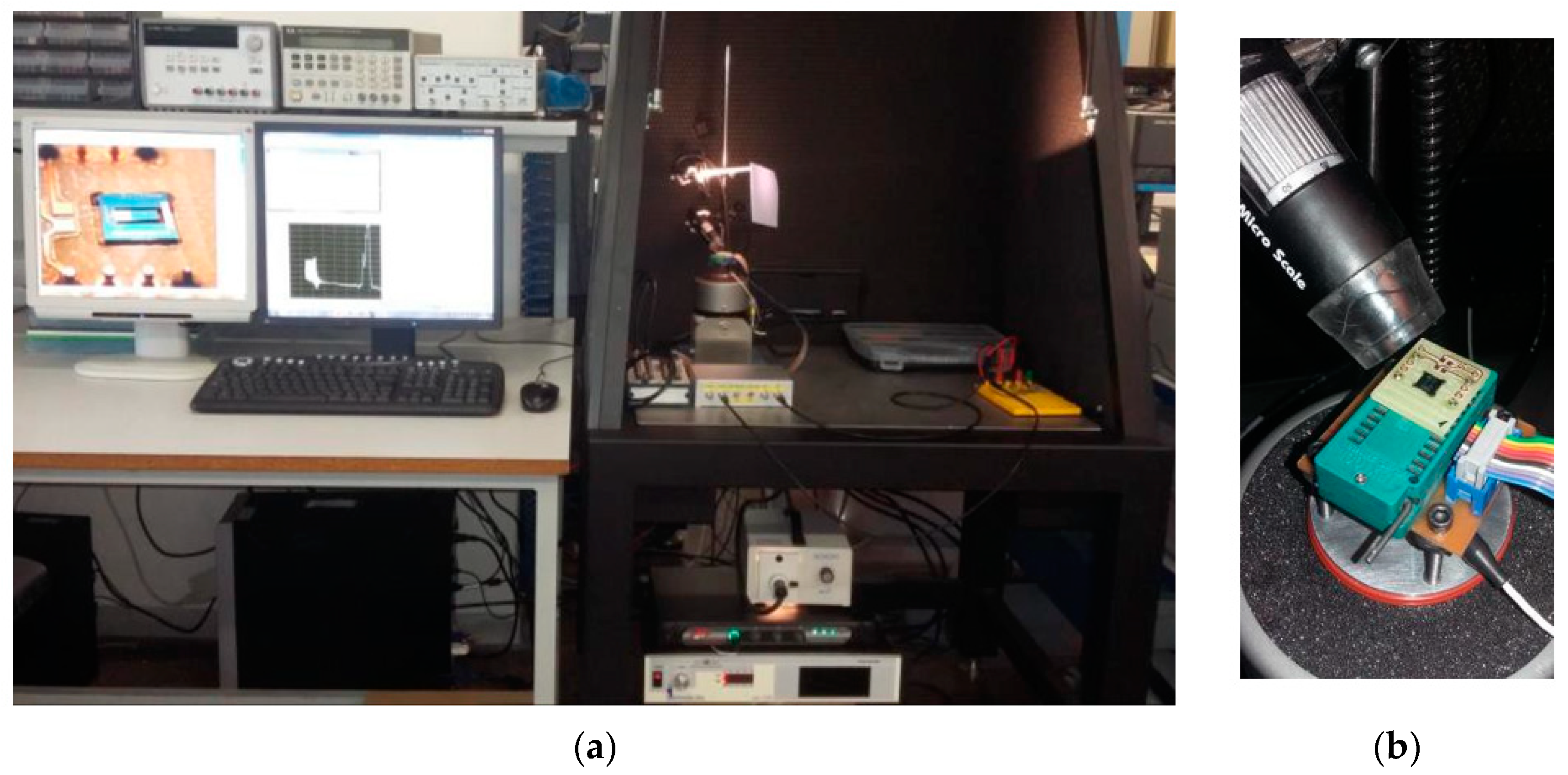
Several devices, shown in the Figure 1c, with different geometries and designs have been manufactured, expecting a high output power density. The electrical characterization is performed by using a shaker (Vibration Testing Controller VR9500), with the acquisition system (National Instruments PCI-6132 and BNC-2110), controlled by an ad-hoc MATLAB program that performs a frequency sweep with different specific accelerations (Figure 2a). For instance, the volume of one of these devices is 12.9 mm3 for the complete chip and 4.1 mm3 for the cantilever beam (Figure 2b). The final power density for this energy harvester is expected to be greater than 250 µW/cm3.
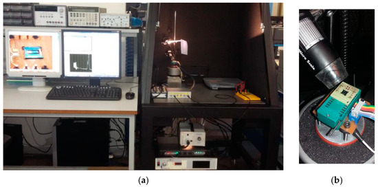
Figure 2.
(a) Characterization configuration of the piezoelectric MEMS generating devices; (b) Fabricated piezoelectric microgenerator bonded to a PCB and mounted on the shaker.
3. Converter Circuit
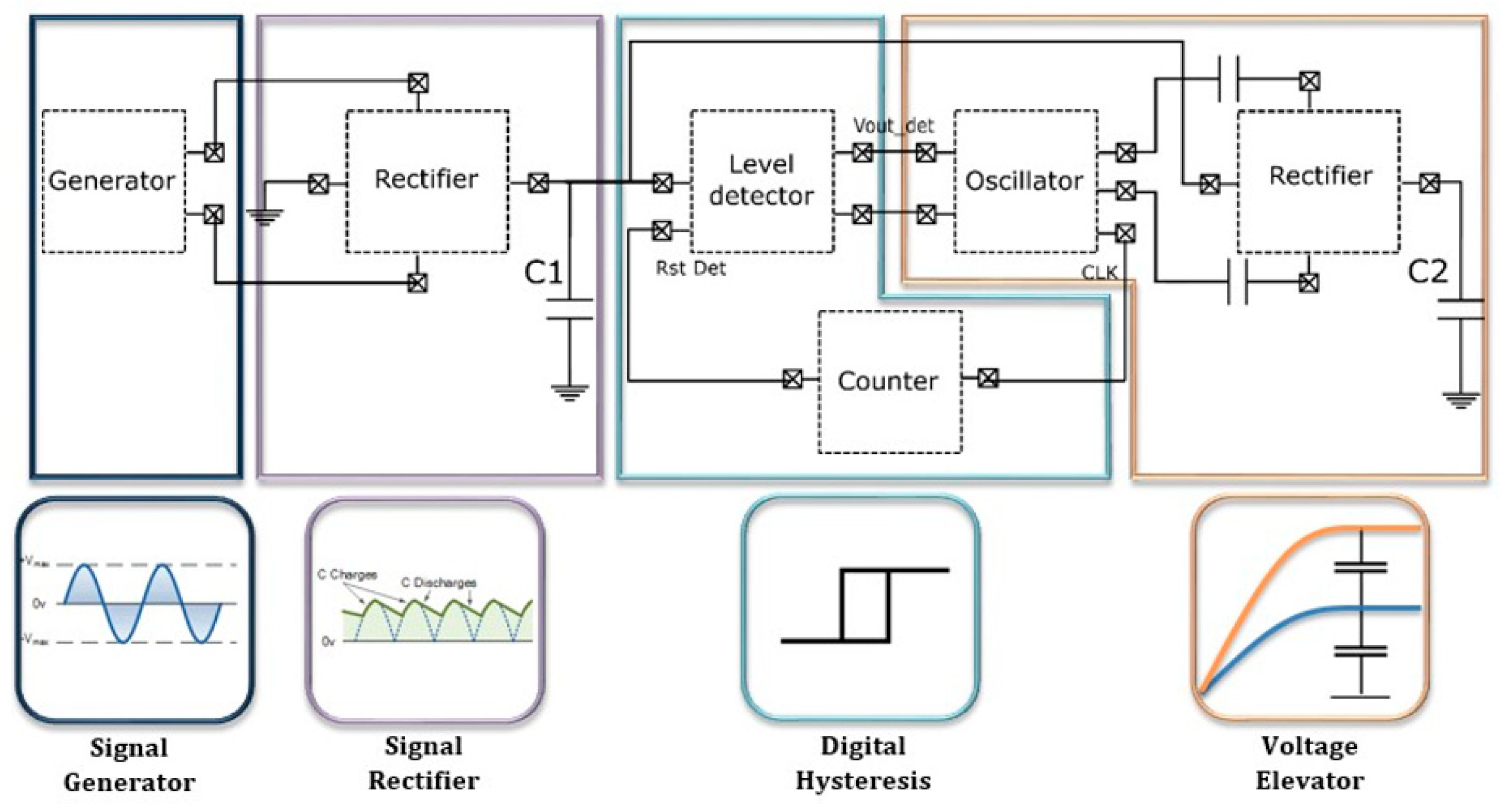
To be able to use the energy generated by the energy harvester, a power conditioning circuit is needed. This circuit must be fully integrable and able to power the nodes of WSNs. For these reasons, our proposed circuit is a charge pump that collects the harvested charges and increases the output voltage to the needed by the application circuit. Charge pumps, also known as inductor less DC/DC, are not the most efficient circuits but they are fully integrable. Our converter circuit includes a level detector and a counter to avoid the energy consumption while charging the first store capacitor.
We have designed our converter by using CADENCE-Virtuoso 6.1.6—64b and the technology Silterra C18G—180 nm CMOS logic 1.8 V/3.3 V. Silterra technology offers an optimal combination of performance in terms of power, speed and gates density. Furthermore, they are working on the integration of piezoelectric materials (AlN) in their standard CMOS technology.
The circuit, shown in Figure 3, is composed by different blocks. The generator block is a model of the equivalent circuit of our piezoelectric microgenerator, based on the work of S. Roundy [5]. This block generates an AC signal. The rectifier block, convert this alternating signal into a DC signal and start charging the first capacitor (C1). The level detector waits for a certain threshold voltage in the first capacitor to power the oscillator once reached. Then, the oscillator converts the DC voltage stored in the first capacitor into a square alternating signal. The outputs of the oscillator are connected to another rectifier through two capacitors. In this way, the signal is again rectified but the voltage in the second capacitor is doubled. The counter block is used to reset the level detector every n cycles of the oscillator. It is utilized as timer to let the capacitor to be charged again [6,7].
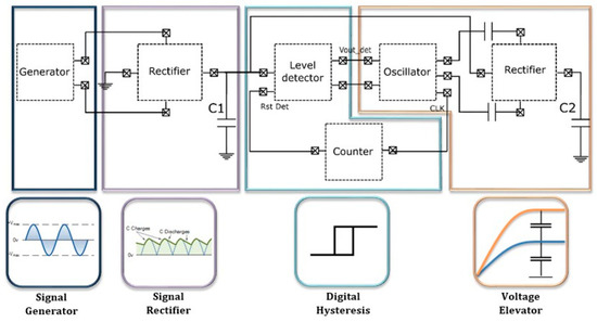
Figure 3.
Schematic of converter circuit, showing the different function block.
Depending on the supply voltage that the application circuit could need, several rectifier stages can be incorporated to reach the desired output voltage. However, the main drawback of adding rectifier stages is that each time we transfer the energy from one capacitor to another, half of the energy is lost.
4. Conclusions
We propose the development of energy harvesters monolithically integrated with power management circuits and storage capacitors in a CMOS-compatible technology. Our idea is to take advantage of the silicon area on top of the cantilever and the rest of the chip to add the integrated circuits and capacitors (Figure 4). This work paves the way to the future development of autonomous smart dust, composed of fully-integrated single microchips that could harvest energy from their environment.
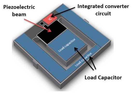
Figure 4.
Diagram of the proposed monolithic system, composed by the converter circuit, capacitors and the piezoelectric MEMS structure for energy harvesting.
Author Contributions
G.M. provided the main idea of the designs of the energy harvesters and the fully monolithically integrated system; E.L performed the simulations to optimize the designs of the energy harvesters; M.D. and J.C. designed and simulated the converter circuit; M.D. performed the characterization of the harvesters; M.D. and G.M. wrote and reviewed the document; G.M. and J.E. contributed to the discussion of the obtained data and to the final version of the manuscript;
Acknowledgments
The authors M. Duque and G. Murillo from the Instituto de Microelectrónica de Barcelona would like to thank the financial support of EnSO project (Energy for Smart Objects), Contract No. 692482.
Conflicts of Interest
The authors declare no conflict of interest.
References
- Tan, Y.K. Energy Harvesting Autonomous Sensor Systems: Design, Analysis, and Practical Implementation, 1st ed.; CRC Press: Boca Raton, FL, USA, 2013. [Google Scholar]
- Murillo, G.; Agusti, J.; Abadal, G. Self-suspended vibration-driven energy harvesting chip for power density maximization. Smart Mater. Struct. 2015, 24, 115027. [Google Scholar] [CrossRef]
- Fang, H.B.; Liu, J.Q.; Xu, Z.Y.; Chen, D.; Cai, B.C. Fabrication and performance of a MEMS-based piezoelectric power generator for vibration energy harvesting. Microelectron 2006, 37, 1280–1284. [Google Scholar] [CrossRef]
- Murillo, G.; Duque, M.; Leon, E.; Navarro, M.; Martinez, C.; Esteve, J. Vibration-driven Energy Harvesting for Smart Objects. In Proceedings of the 43rd International conference on Micro and Nanoengineering, Braga, Portugal, 18–22 September 2017. [Google Scholar]
- Roundy, S.; Wright, P.K. A piezoelectric vibration based generator for wireless electronics. Smart Mater. Struct. 2004, 13, 1131–1142. [Google Scholar] [CrossRef]
- Uyemura, J.P. Circuit Design for CMOS VLSI, 1st ed.; Springer: New York, NY, USA, 1992. [Google Scholar]
- Allen, P.E.; Holberg, D.R. CMOS Analog Circuit Design, 2nd ed.; Oxford University: Oxford, UK, 2002. [Google Scholar]

Publisher’s Note: MDPI stays neutral with regard to jurisdictional claims in published maps and institutional affiliations. |
© 2018 by the authors; Licensee MDPI, Basel, Switzerland. This article is an open access article distributed under the terms and conditions of the Creative Commons Attribution (CC BY) license (http://creativecommons.org/licenses/by/4.0/).