Proceeding Paper

Optimization in the Design and Fabrication of a PZT Piezoelectric Micromachined Ultrasound Transducer (PMUT) †

Department of Electrical Engineering (ESAT-MICAS), KU Leuven, 3001 Leuven, Belgium
*
Author to whom correspondence should be addressed.
Presented at the Eurosensors 2018 Conference, Graz, Austria, 9–12 September 2018.
Proceedings 2018, 2(13), 743; https://doi.org/10.3390/proceedings2130743
Published: 29 November 2018
(This article belongs to the Proceedings of EUROSENSORS 2018)

Abstract

:
This paper presents an optimized way of lead zirconate titanate (PZT) deposition in order to selectively grow three different (100/001), (110), and (111) crystal orientation in two different thickness ranges, thinner and thicker than 400 nm. The thickness of the PZT layer is also optimized to not diminish the generated bending moment more than 10%. A 1μm PZT layer with (100/001) dominant crystal orientation and highly columnar crystal structure is deposited and used in the fabrication of a circular PMUT. The PMUT has a 410 μm diameter and resonates at 462 kHz with the displacement of 1200 nm/V.

1. Introduction

In recent years, there has been increased interest in piezoelectric micromachined ultrasound transducers (PMUTs) in many applications, such as bio-medical ultrasonic imaging, finger print sensors, and range finders [1,2,3]. Lead zirconate titanate (PZT), because of its high piezoelectric coefficient and relatively easy deposition process, is the most common piezoelectric thin-film. The quality and, likely, the piezoelectric coefficient of the PZT thin-film is inherently linked to its crystal orientation and structure. In recent years, there has been research on the optimization of PZT properties to suit the needs of specific device performance [4,5]. Due to the fact that selectively growing a specific PZT crystal orientation is not a trivial process, in most cases, a mixed crystal orientation is acceptable. However, this will affect the piezoelectric coefficient of the PZT layer.
In this research we optimized the thickness and the deposition process of a PZT thin-film by sol-gel method (12% PZT 110/52/48 sol-gel solution, Mitsubishi Materials Corporation) in order to control the grow in three different (100/001), (110), and (111) crystal orientation. Finally, a PMUT is fabricated and measured to investigate the functionality of the deposited PZT layer.

2. Material and Methods

A PZT thin-film was deposited by the sol-gel method on a Si/SiO2(600 nm)/Ti(20 nm)/Pt(200 nm) substrate. Table 1 shows the different recipes that were used. Overall, the PZT solution was spin- coated and subsequently pyrolyzed at specific temperature for 5 minutes, and this cycle was repeated several times. After 3 to 4 such cycles, a rapid thermal annealing process at 700 °C was introduced to render the PZT layer in a perovskite crystalline phase. The number of cycles is indicated in Table 1 as “RTP after # step”. The ramp-rate of the RTP is mentioned as well. This process was repeated until the desired thickness was obtained. The recipes can be divided into two main categories; with and without seed layer. By using a seed layer, one PZT layer from the same sol-gel solution was spin-coated, pyrolyzed and rapid thermally annealed before starting the repetitive deposition steps. The recipe of the seed layer deposition is explained in the footer of Table 1. The deposition process is shown in Figure 1a.
In order to measure the functionality of the deposited PZT thin-film, a PMUT was fabricated based on a deep reactive ion etching (DRIE) process on SOI wafers. Figure 1b illustrates the fabrication process.

3. Results and Discussion

3.1. PZT Crystal Characterization

3.1.1. Less Than 400 nm Thick PZT Layer

The XRD patterns of 360nm thick PZT layers with the first 3 recipes are shown in Figure 2a. The PZT deposition without seed layer leads to a mixed orientation of (111) and (110). Moreover, a slow spin-coating speed tends to improve the (100/001) crystal orientation. Figure 2b shows the crystal orientation of PZT4 and PZT5, in which a seed layer with 1 K/s and 2 K/s RTP ramp-rate were used, respectively. The (100/001) and (111) crystal orientations in both recipes were dominant, but in PZT5, which the RTP ramp-rate was 2 K/s, the intensity of the (100/001) peak was higher. The XRD pattern of PZT6 up to PZT9 recipes are shown in Figure 2c. According to the results of Figure 2b,c, three inferences can be deduced: (1) a low RTP ramp-rate (<6 K/s), in both the seed layer and multi-coated layers, helps to improve the (100/001) crystal orientation. As a result, in order to amplify the (100/001) orientation peak, recipe PZT10, in which the RTP ramp-rate of the multi-coated layers was lowered to 2 K/s, was tried and the improvement in its XRD pattern is shown in Figure 3a; (2) PZT (110) crystal orientation can be grown by a 5 K/s RTP on the seed layer and a 10 K/s RTP or faster on the multi-coated layers; (3) the PZT thin-film can be deposited with a dominant (111) crystal orientation, if the seed layer and multi-coated layers are annealed rapidly with a ramp-rate of 10 K/s.

3.1.2. More Than 400 nm up to 1 μm Thick PZT Layer

By depositing a PZT layer with the thickness of 1μm only two crystal orientations had the tendency to appear. In the case with a seed layer, (100/001) was the dominant orientation. Otherwise, the PZT thin-film was more (110) textured. Due to the (111) crystal orientation of the Pt layer, the grown PZT layer had always some (111) texture, as shown in Figure 3a. The cross-section SEM image of 600 nm PZT1 and 1 μm PZT6 is shown in Figure 3b,c, respectively. Both samples had a columnar crystal structure, but PZT6 was more columnar which indicates the higher piezoelectric response of the (100/001) orientation with respect to the other orientations [6].

3.2. PZT Thickness Optimization

By increasing the thickness of the PZT layer, the crystal property of the PZT and the position of the neutral axis in the Si/PZT membrane vary. As shown in the bottom of Figure 3b,c, by increasing thickness, the grain size increases and the crystal structure becomes more columnar. The columnar structure helps to improve the piezoelectric coefficient and bigger grain size decreases the leakage current. On the other hand, by increasing the thickness, the position of the neutral plane in the Si/PZT membrane is moving towards the center of the PZT layer, which degrades the bending moment, since the lower part of the PZT works against the upper part. This is due to the fact that the bending moment is linearly related to the distance from the PZT midplane to the neutral plane [7]. Equation (1) gives the distance between the PZT midplane and neutral plane:
  D = ( t s i + t p z t 2 ) ( 1 2 ( E s i t s i 2 + E p z t ( ( t s i + t p z t ) 2 t s i 2 ) E s i t s i + E p z t t p z t ) ,
where, tsi, tpzt, Esi, and Epzt are the Si membrane and PZT layer thickness, and silicon and PZT Young’s modulus, respectively. In order to not change the position of the neutral plane more than 10%, a PZT layer with the maximum thickness of 1 μm should be chosen for a 6 μm silicon membrane.

3.3. Fabricated PMUT Characterization

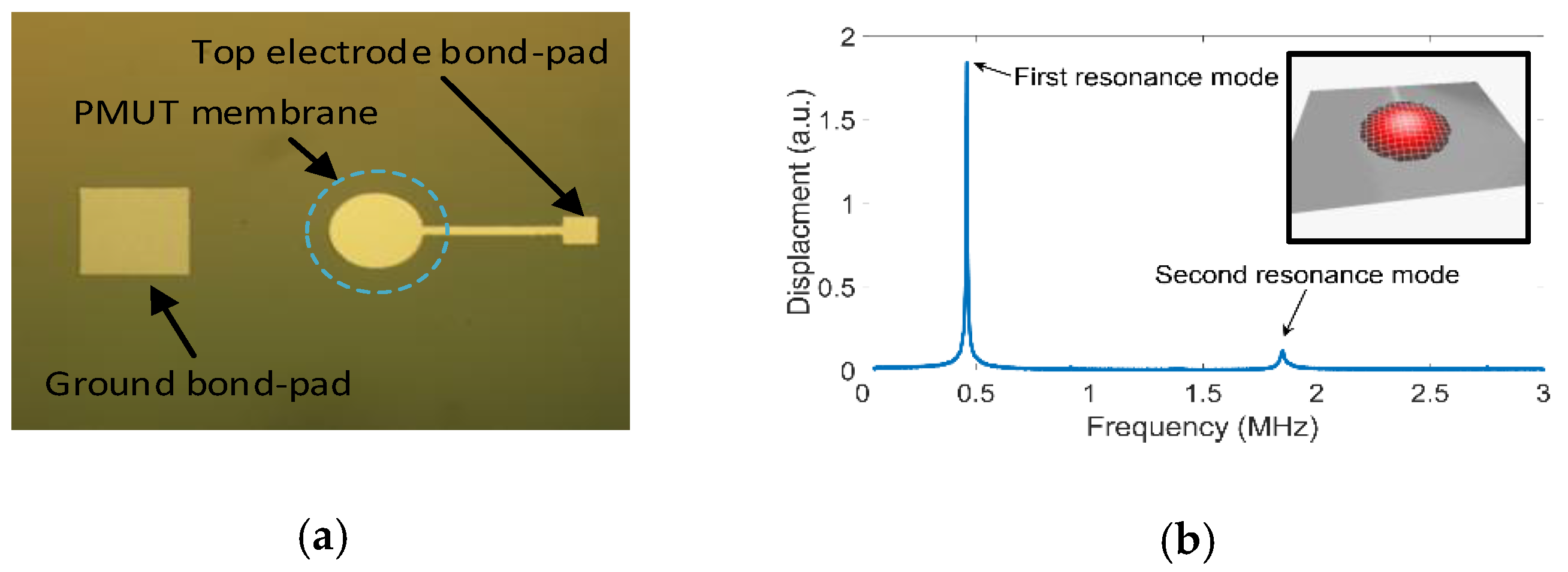
As explained in Section 2, a PMUT was fabricated by depositing a 1 μm PZT10 layer, with a dominant (100/001) crystal orientation. The fabricated circular PMUT has 410 μm diameter and the thickness of the silicon membrane is 6 μm. Figure 4a shows the optical microscopic image of the PMUT. The resonance frequency (462 kHz) and the amplitude were measured by a laser doppler vibrometer (LDV) (Polytec, MSA-500, Waldbronn, Germany) and is shown in Figure 4b. The obtained displacement was 1200 nm/V.

4. Conclusions

An optimized deposition method of PZT thin-films by a sol-gel process has been proposed in order to grow three different (100/001), (110), and (111) crystal orientations. A seed layer is used to guide the crystal orientation of the posterior deposited layers. Unlike the existing reports in literature, the seed layer in this research is from the same sol-gel solution used for the main PZT deposition. An equation is also derived, from which the optimum thickness of the PZT layer can be found to not diminish the generated bending moment more than 10%. A 1μm deposited PZT layer with dominant (100/001) orientation and highly columnar structured is used to fabricate a circular PMUT with 410 μm diameter. The PMUT has 462 kHz resonance frequency and a large 1200 nm/V displacement.

Acknowledgments

This work was supported by the European Union’s Horizon 2020 research and innovation program under grant agreement No 665347.

Conflicts of Interest

The authors declare no conflict of interest.

References

  1. Jung, J.; Lee, W.; Kang, W.; Shin, E.; Ryu, J.; Choi, H. Review of piezoelectric micromachined ultrasonic transducers and their applications. J. Micromech. Microeng. 2017, 27, 113001. [Google Scholar] [CrossRef]
  2. Sadeghpour, S.; Pobedinskas, P.; Haenen, K.; Puers, R. A Piezoelectric Micromachined Ultrasound Transducers (pMUT) Array, for Wide Bandwidth Underwater Communication Applications. Proceedings 2017, 1, 364. [Google Scholar]
  3. Sadeghpour, S.; Meyers, S.; Kruth, J.-P.; Vleugels, J.; Puers, R. Single-Element Omnidirectional Piezoelectric Ultrasound Transducer for under Water Communication. Proceedings 2017, 1, 363. [Google Scholar] [CrossRef]
  4. Sama, N.; Herdier, R.; Jenkins, D.; Soyer, C.; Remiens, D.; Detalle, M.; Bouregba, R. On the influence of the top and bottom electrodes—A comparative study between Pt and LNO electrodes for PZT thin film. J. Cryst. Growth 2008, 310, 3299–3302. [Google Scholar] [CrossRef]
  5. Sadeghpour, S.; Ceyssens, F.; Puers, R. Crystalline growth of AlN thin films by atomic layer deposition. J. Phys. Conf. Ser. 2016, 757, 012003. [Google Scholar] [CrossRef]
  6. Sanchez, L.M.; Potrepka, D.M.; Fox, G.R.; Takeuchi, I.; Wang, K.; Bendersky, L.A.; Polcawich, R.G. Optimization of PbTiO3 seed layers and Pt metallization for PZT-based piezoMEMS actuators. J. Mater. Res. 2013, 28, 1920–1931. [Google Scholar] [CrossRef]
  7. Shelton, S.; Chan, M.-L.; Park, H.; Horsley, D.; Boser, B.; Izyumin, I.; Przybyla, R.; Frey, T.; Judy, M.; Nunan, K.; et al. CMOS-Compatible AlN Piezoelectric Micromachined Ultrasonic Transducers. In Proceedings of the 2009 IEEE International Ultrasonics Symposium, Rome, Italy, 20–23 September 2009; pp. 402–405. [Google Scholar]
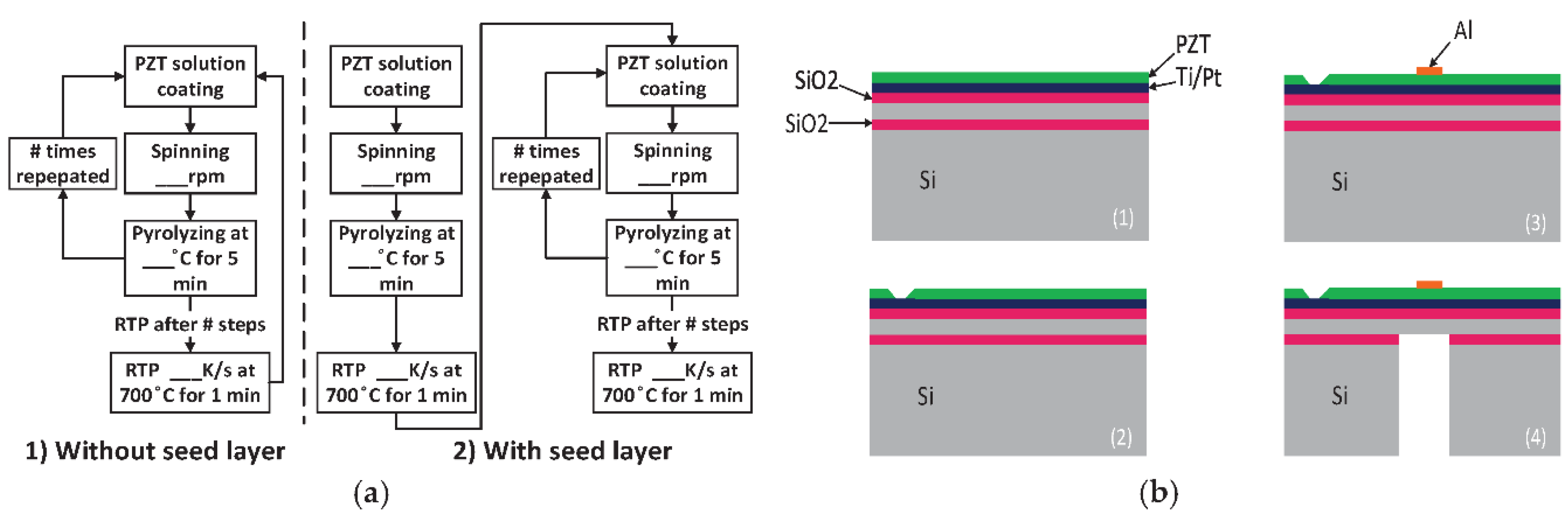
Figure 1. (a) Process flowchart of the PZT deposition (1) without and (2) with a seed layer deposition; (b) The fabrication process: (1) Deposition of the SiO2/Ti/Pt and PZT layer. The SiO2 was deposited by wet thermal process as an isolation layer; (2) patterning of the PZT layer to access the bottom electrode. (3) Deposition and patterning of the top electrode. (4) Deep Reactive Ion Etching (DRIE) to release the PMUT membrane. (all electrodes were deposited by RF sputtering).
Proceedings 02 00743 g001
Figure 2. XRD pattern of samples PZT1 to PZT9 (all samples have less than 400 nm thickness).
Proceedings 02 00743 g002
Figure 3. (a) XRD pattern of samples PZT5 and PZT10 (400 nm), PZT6 (1 μm), and PZT1 (600 nm); (b) cross-section (top) and surface (bottom) SEM images of 600 nm PZT1 and (c) 1 μm PZT6.
Proceedings 02 00743 g003
Figure 4. (a) The optical microscopic image of the fabricated PMUT; (b) the measured frequency response and the measured deflection (inlet) by LDV.
Proceedings 02 00743 g004
Table 1. The parameters of different recipes used for the PZT deposition.
RecipeSeed LayerSpin-Coating Speed (rpm)Pyrolysis Temperature (°C)RTP after # StepsRTP Ramp Rate (K/s)
PZT1No3000330310
PZT2No2000330310
PZT3No30003303100
PZT4Seed layer 1 (x = 1 K/s) 12000300410
PZT5Seed layer 2 (x = 2 K/s) 12000300410
PZT6Seed layer 3 (x = 5 K/s) 12000300410
PZT7Seed layer 4 (x = 6 K/s) 12000300410
PZT8Seed layer 5 (x = 10 K/s) 12000300410
PZT9Seed layer 6 (x = 100 K/s) 12000300410
PZT10Seed layer 2 (x = 2 K/s) 1200030042
1 Seed layer recipe: 2000 rpm spin-coating 200 °C 5min HP pyrolyze RTP x K/s at 700 °C for 1 min.
Publisher’s Note: MDPI stays neutral with regard to jurisdictional claims in published maps and institutional affiliations.