Proceeding Paper

Miniaturized Coplanar Waveguide for Nanostructured Magnetostrictive Multilayer Characterization †

by
Abdelhatif El Fellahi
,
Aurélien Mazzamurro
,
Jean Claude Gerbedoen
,
Yannick Dusch
,
Olivier Bou Matar
,
Phillippe Pernod
,
Abdelkrim Talbi
and
Nicolas Tiercelin
*
Univ-Lille, CNRS, Centrale Lille, ISEN, Univ-Valenciennes, IEMN UMR 8520 - LIA LICS/LEMAC, F-59000 Lille, France
*
Author to whom correspondence should be addressed.
Presented at the Eurosensors 2018 Conference, Graz, Austria, 9–12 September 2018.
Proceedings 2018, 2(13), 851; https://doi.org/10.3390/proceedings2130851
Published: 17 January 2019
(This article belongs to the Proceedings of EUROSENSORS 2018)

Abstract

:
A miniaturized coplanar waveguide (CPW) on a Y-cut LiNbO3 substrate operating in Radio Frequency region (RF) is proposed for studying of magnetostrictive multi-layered structure. The structure is composed of a 14 × [TbCo2 (3.7 nm)/FeCo (4 nm)] nanostructured multi-layer. Using microtechnology process, the miniaturized CPW has been designed with a 50 µm wide signal line in the frequency range from 6 MHz to 6 GHz. Electromagnetic simulations based on ®Ansys/HFSS demonstrate insertion losses less than 2 dB and show that the magnetic field is more confined in the nanostructured multi-layer placed on top of the micro-sized CPW. By using Vectorial Network Analyzer (VNA) the Ferromagnetic Resonance (FMR) is investigated from the reflection (Sii) or transmission (Sij) coefficients of scattering parameters. An inversion model is finally used to extract the complex permeability spectrum of the thin-film in a large frequency range.

1. Introduction

Recent works in our study area demonstrate the great interest of multilayered piezoelectric-piezomagnetic composites in the development of Surface Acoustic Waves (SAW) sensors. It was shown that in magnetoelastic films exhibiting in-plane uniaxial anisotropy, a high susceptibility to the external driving field can be obtained in the vicinity of a field-induced Spin Reorientation Transition (SRT) [1,2]. Their large magnetoelectric coefficient, compared to one of the single-phase materials, will allow the development of sensitive sensors. Nevertheless, a reliable and authentic value of the permeability is very important for such applications. FMR based on a VNA and CPW has become a common experimental tool for studying magnetic films [3]. However, the necessity for an accurate and localized characterization of these materials in terms of electric and magnetic properties is still needed.
For this reason, we present here a method that is based on a miniaturized CPW on a Y-cut LiNbO3 enabling here broadband measurement of RF scattering parameters. The set-up description is given in Section 2. Preliminary results are presented in Section 3.

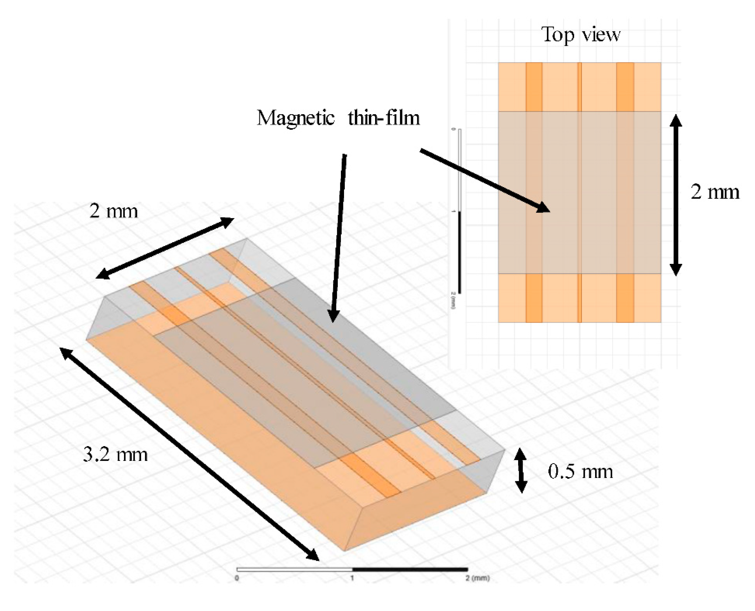
2. Set-Up Description

The miniaturized coplanar line topology is designed for frequencies up to 6 GHz on a 500 μm thick Y-cut LiNbO3 substrate in order to investigate a nanostructured magnetostrictive thin film. The coplanar line technology consists of three gold metal lines deposited on the substrate. The dimensions are a 50 μm wide signal line and a 435 μm gap as shown in Figure 1.
From an electromagnetic point of view, the miniaturized waveguide is adopted to confine the fields in the magnetic-film.
A 2 mm wide and 107 nm thick 14 × [TbCo2 (3.7 nm)/FeCo (4 nm)] thin film is deposited by RF-Sputtering on the miniaturized CPW. A magnetic easy axis (EA) is obtained in the magnetic layer by applying a magnetic field during deposition [4]. A thin layer of photoresist insulates the film from the CPW.
The fabrication of the miniaturized test structure is based on standard microtechnological processes. Scanning Electron Microscope (SEM) images of the fabricated structure are given in Figure 2. The pictures show that the nanostructured thin-film was successfully deposited by RF-Sputtering with the CPW line underneath. As an illustration, cross-sectional transmission electron microscopy (TEM) images of the nanostructured uni-axial multi-layer structure deposited on a silicium wafer are given in Figure 3.

3. RF Simulation

Electromagnetic simulations based on ®Ansys/HFSS allow to extract S-parameters. In Figure 4, we present the simulation of the reflection coefficient and the transmission coefficient in free-space conditions up to 6 GHz. We can note that the return loss is better than −20 dB. Also, the results demonstrate insertion losses less than 2 dB over the frequency range. These preliminary results are hopeful up to 6 GHz.

4. Conclusions

In order to investigate nanostructured magnetostrictive multilayers, a miniaturized coplanar waveguide based on the interaction of a magnetic thin-film with electromagnetic waves at gigahertz frequencies was developed. The structure was designed using Electromagnetic simulations based on (®Ansys/HFSS). Preliminary results have been given and demonstrate insertion losses less than 2 dB over the frequency range. Also, SEM images show the success of the realization in clean room. In the future works, the magnetization of the nanostructured TbCo2/FeCo thin film will be measured with a Vibrating Sampling Magnetometer (VSM). Also, by using Vectorial Network Analyzer the experimental Ferromagnetic Resonance spectra will be extracted for different external magnetic fields. Finally, from the scattering parameters the effective impedance arising from the sample magnetic response (i.e., permeability) of the sample will be determined.

Funding

This research was supported by the RENATECH network and Centrale Lille.

Conflicts of Interest

The authors declare no conflict of interest.

References

  1. Tiercelin, N.; Talbi, A.; Preobrazhensky, V.; Pernod, P.; Mortet, V.; Haenen, K.; Soltani, A. Magnetoelectric effect near spin reorientation transition in giant magnetostrictive-aluminum nitride thin film structure. Appl. Phys. Lett. 2008, 93, 162902. [Google Scholar] [CrossRef]
  2. Zhou, H.; Talbi, A.; Tiercelin, N.; Bou Matar, O. Multilayer magnetostrictive structure based surface acoustic wave devices. Appl. Phys. Lett. 2014, 104, 114101. [Google Scholar] [CrossRef]
  3. Głowiński, H.; Schmidt, M.; Gościańska, I.; Ansermet, J.P.; Dubowik, J. Coplanar waveguide based ferromagnetic resonance in ultrathin film magnetic nanostructures: Impact of conducting layers. J. Appl. Phys. 2014, 116, 053901. [Google Scholar] [CrossRef]
  4. BenYoussef, J.; Tiercelin, N.; Petit, F.; Le Gall, H.; Preobrazhensky, V.; Pernod, P. Statics and dynamics in giant magnetostrictive TbxFe1−x/Fe0.6/Co0.4 multilayers for MEMS. IEEE Trans. Magn. 2002, 38, 2817–2819. [Google Scholar]
Figure 1. Schematic representation of the miniaturized CPW showing the location of the 107 nm thick 14 × [TbCo2 (3.7 nm)/FeCo (4 nm)] nanostructured multi-layer under test. The inset is a top view.
Proceedings 02 00851 g001
Figure 2. (a) SEM, image of the 14×[TbCo2 (3.7 nm)/FeCo (4 nm)] deposited on a CPW. (b) Zoom-in on the nanostructured multi-layer thin-film.
Proceedings 02 00851 g002
Figure 3. (a) TEM, cross-section image of the of a 14 × [TbCo2 (3.7 nm)/FeCo (4 nm)] nanostructured multi-layer. (b) A zoom-in.
Proceedings 02 00851 g003
Figure 4. S-parameters recorded in the frequency range from 60 MHz to 6 GHz. (®Ansys/HFSS—S11—S21).
Proceedings 02 00851 g004
Publisher’s Note: MDPI stays neutral with regard to jurisdictional claims in published maps and institutional affiliations.

