Abstract
ZnO nanorods (NRs) arrays with good vertical alignment were selectively grown on microscale patterned surfaces by a MEMS-compatible, low-temperature chemical-bath deposition method (CBD). The direct-current (DC) sputtered and subsequently annealed ZnO seed-layer was found to have a crucial effect on the ZnO NRs growth. Depending on the pre-annealing temperature between 200 °C and 700 °C, which is compatible with our microcantilever fabrication process, diameters and area densities of the NRs of 60–99 nm and 17–27 µm−2 were observed, respectively, with the best alignment at 600 °C. A surface-area enlargement factor of 48 was achieved with respect to a ZnO layer indicating the potential of ZnO NRs arrays for MEMS applications, such as gas sensing.
1. Introduction
In recent years, one-dimensional (1D) ZnO nanostructures have received great interest due to their potential applications in electronic and optoelectronic devices, such as solar cells, gas sensors, photodetectors, light-emitting diodes and surface acoustic wave devices. Various methods have been studied to fabricate aligned 1D ZnO nanostructures, including thermal vacuum evaporation (TVE), electron beam gun evaporation, molecular beam epitaxy (MBE), metal–organic chemical vapor deposition (MOCVD), sputtering techniques, chemical bath deposition (CBD), etc. [1].
However, for the moment, it is still challenging to achieve the growth of functional ZnO nanostructures with highly aligned and oriented arrays on micro and nanoscale surfaces, which are crucial for the performance of these devices. The low-temperature CBD method is a simple facility, no-catalyst and low-cost process [2]. However, before the growth of ZnO NRs, an aqueous spin-coating method or sol-gel alkaline solution is essential for seed-layer (SL) coating, which are not compatible with MEMS fabrication [3]. In this paper, we report a CBD-based two-steps process, by using a DC sputtering/annealing (S/A) method for SL deposition. The area-selective growth of aligned ZnO nanorods (NRs) arrays was achieved on n-type silicon microcantilevers, indicating its applicability for MEMS device fabrication. In comparison with a sol-gel seed-layer deposition method, the DC-sputtered ZnO seed-layer has some advantages, such as easy thickness control, good morphology and high process repeatability. Compared with radio frequency (RF) magnetron-sputtering, which has a base pressure about 9 × 10⁻⁵ Pa and a working Ar pressure of 5 × 10⁻³ Pa [2], DC-sputtering can be operated at a moderate working pressure of 640 Pa, and has a much lower power consumption. Furthermore, it has been found that the properties of ZnO NRs have a dependence on the pre-annealing of the seed-layer either by sol-gel deposition or by RF magnetron sputtering, so in this paper, DC-sputtered Zinc films were annealed under different temperatures to prepare seed-layers for subsequent ZnO NRs growth by CBD. We find that the crystallinity, resistivity and morphology of the ZnO NRs strongly depend on the pre-annealing of the seed-layers.
2. Experimental
Area-Selective Growth of Aligned ZnO Nanorods Arrays
Figure 1 depicts the fabrication process steps of area-selective growth of aligned ZnO nanorods (NRs) arrays on n-type silicon, and the details are described as follows:
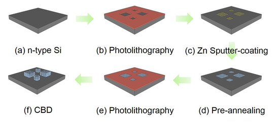
Figure 1.
Schematic diagram of area-selective growth of aligned ZnO nanorods (NRs) on n-type silicon.
- (a)
- The fabrication started from a piece of sample with a dimension of 30 × 30 mm2, the sample was cut from an n-type bulk-silicon wafer (crystal orientation: <100>; resistivity: 1–10 Ω × cm; thickness: 275 ± 15 µm and diameter: 100 ± 0.13 mm) and cleaned by putting the sample into a boiling acid mixture (H2O2 (30%) and H2SO4 (96%), v:v = 1:1) for 5 min.
- (b)
- A positive photoresist (AZ 5214E, Merck, Kenilworth, NJ, USA) was utilized during the subsequent photolithography step and a MJB4 mask aligner (SÜSS MicroTec AG, Garching, Germany) was used to expose the pattern area. Prior to the exposure, the photoresist spin-coating procedure was run at a speed of 5000 rpm for 35 s, to create a homogenous photoresist layer of 1.5 µm in thickness. After the exposure, the sample was then dipped and developed in AZ 726 MIF developer solution (MicroChemicals, Merck) for 60 s, followed by DI water rinsing and nitrogen purging.
- (c)
- Afterwards, a polycrystalline Zn film was prepared by sputtering Zn (99.99%) using high purity Ar (99.99%) gas under 50 µA direct current (DC), at room temperature (25 °C) and a working pressure of 640 Pa. To obtain the selective deposition of sputtering film on the patterned area, the excess ZnO was removed using photoresist lift-off.
- (d)
- Then the sputtered Zn-film was annealed in an oven with open atmosphere, to investigate influence of annealing temperature on the nanorods growth, the sputtered samples were annealed at 200 °C, 300 °C, 400 °C, 500 °C, 600 °C and 700 °C, respectively.
- (e)
- When the seed-layer has been prepared, a subsequent photolithography step was implemented corresponding to step (b) to protect the substrate during the next CBD process.
- (f)
- ZONRs were grown by dipping the sample in an aqueous solution, which consisted of 30 mmol/L zinc nitrate (Zn(NO3)2) and 30 mmol/L hexamethyleneteramine (HMT, C6H12N4), respectively. The deposition was carried out in a temperature-controlled chemical reactor, which was additionally equipped with a thermometer and a reflux condenser, for 3 h at 90 °C. After the reaction, the sample was cleaned with acetone and deionized water, successively [4].
3. Results and Discussion
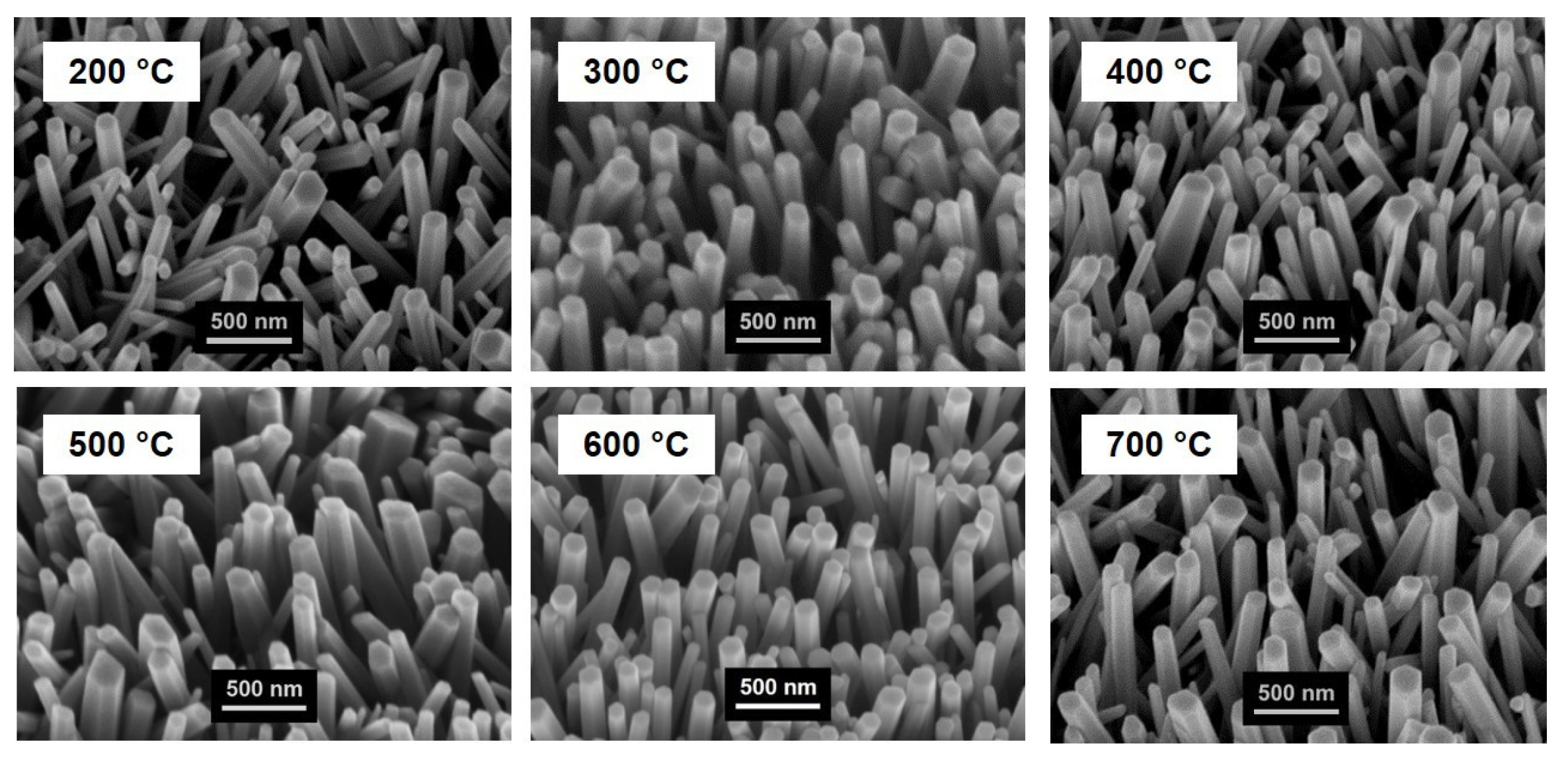
Figure 2 shows the top-view SEM graphs with a tilt angle of 30° of the ZnO NRs grown on the ZnO seed-layers annealed at different temperatures, all the NRs were grown in the chemical bath at 90 °C for 3 h. As it can be seen from the graphs, the obtained ZnO NRs were vertically oriented with respect to the substrates, the NRs based on the seed-layers annealed at 600 °C (NRs-600) tends to have the best orientation.
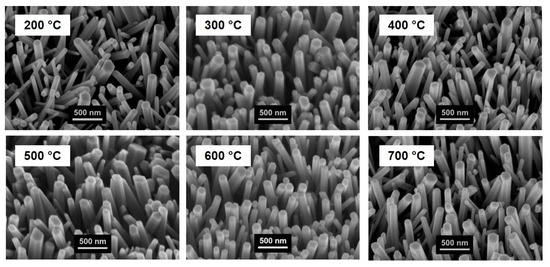
Figure 2.
Inclined-view (30°) SEM graphs of ZnO NRs grown on S/A SLs at different pre-annealing temperatures from 200 °C to 700 °C.
The density and average diameters of the corresponding ZnO NRs on the seed-layers annealed at different temperatures are calculated according to Figure 2 and listed as Table 1. NRs-600 arrays possessing highest density and a relative big diameter, which means high surface-to-volume-ratio and that is important to the improve MEMS devices performance.

Table 1.
Summary of the characterized parameters of NRs grown at different pre-annealing temperature.
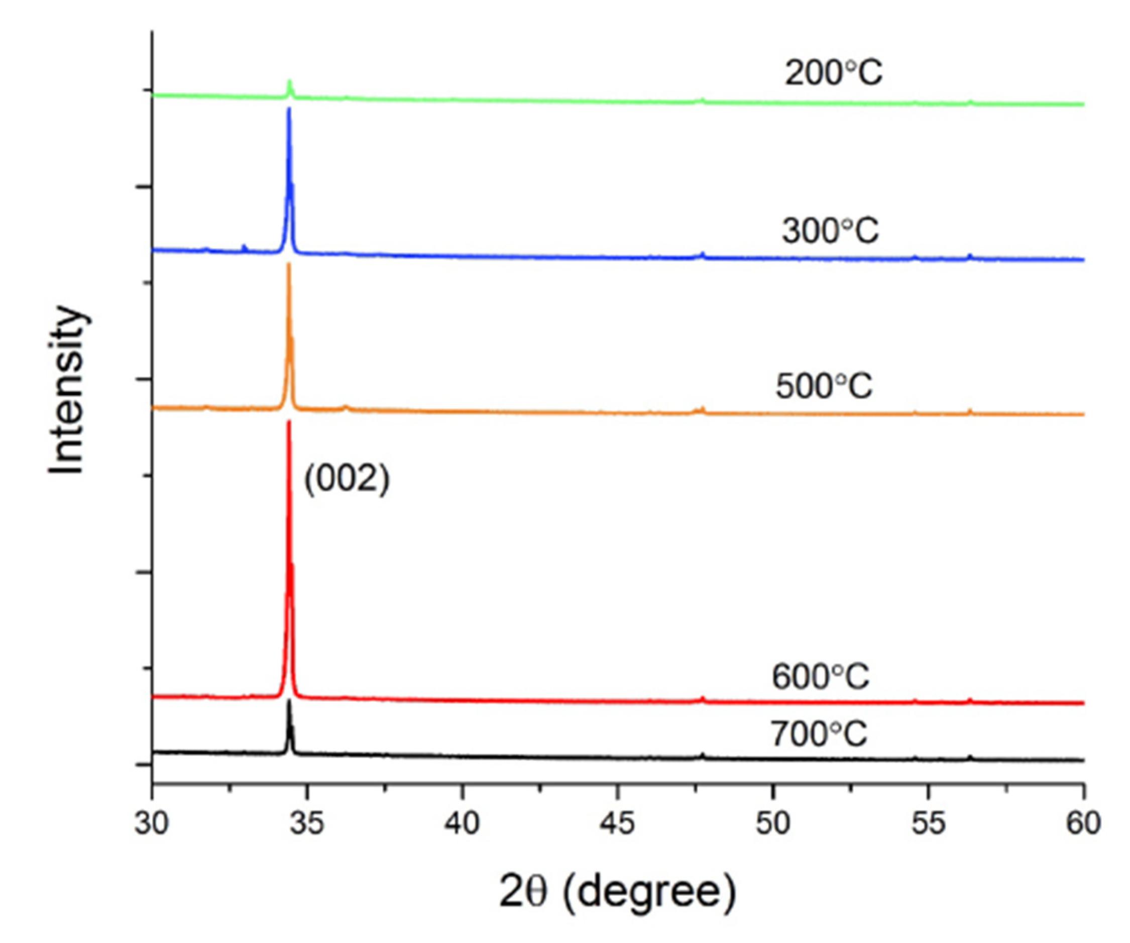
XRD was further used to characterize the crystallinity of different NRs arrays. As shown in Figure 3, the indexed diffraction peaks are consistent with the standard values of the bulk ZnO crystal (JCPDS 36-1451) and all the ZnO NRs have a wurtzite structure. The sharp and strong (002) peak indicates that the ZnO NRs have a potential c-axis orientation on sputtered/annealed ZnO SLs. Besides, we did not observe the (100) and (101) peaks which can be found in some samples grown on the sol-gel seed-layers [5]. The (002) diffraction peak of NRs-600 has the highest intensity, showing that NRs-600 arrays have the highest (002) c-axis orientation preference, revealing the best NRs vertical alignment as Figure 2. Furthermore, the resistivity of ZnO NRs arrays was measured using a four-point probe, and the results are depicted in Figure 4. The observed highest resistivity of the NRs-600 was thought to be caused by their best vertical alignment as visible in Figure 2 and Figure 3.

Figure 3.
XRD spectra of ZnO NRs grown on SLs pre-annealed at different temperatures.
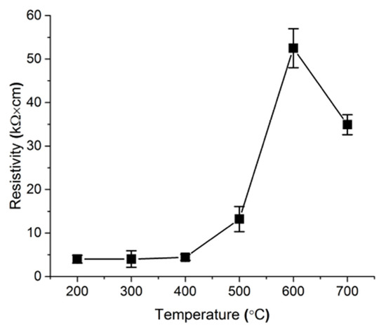
Figure 4.
Resistivity of ZnO NRs array grown on a SL annealed at different temperatures.
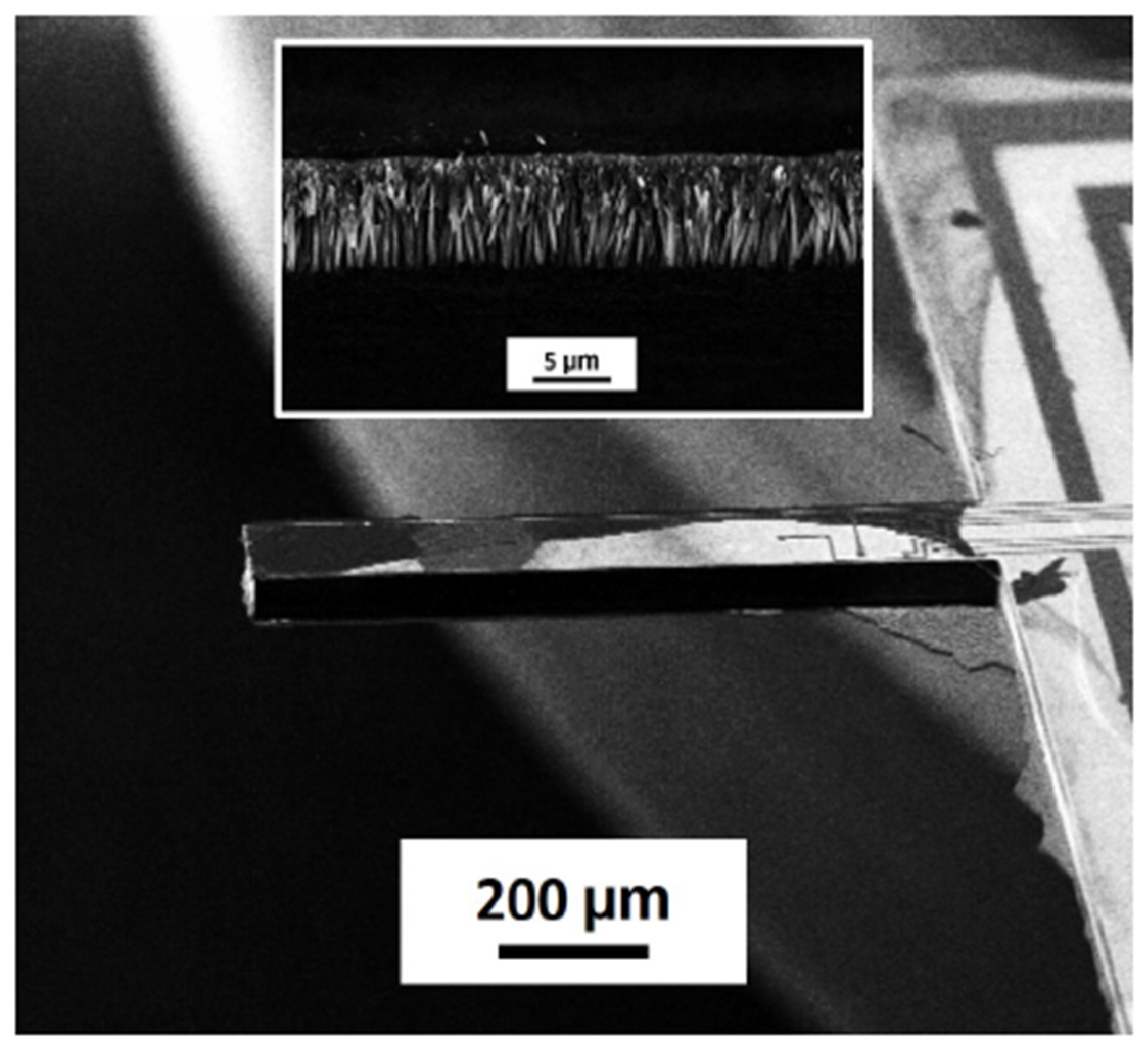
We reported the fabrication and humidity sensing performance of ZnO-NRs-patterned piezoresistive silicon MEMS microcantilevers [6], based on the aforementioned two-step deposition method. In the present study, ZnO NRs were coated on the back surface of the microcantilevers, a schematic and SEM graphs of a microcantilever coated with NRs of 6 µm in length solely on its back surface was displayed in Figure 5 and Figure 6, respectively. A surface-area enlargement factor of 48 was found, indicating its considerable application potential for MEMS devices.
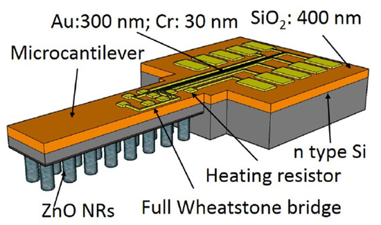
Figure 5.
Schematic graph of a silicon microcantilever patterned with ZnO NRs on its back surface.
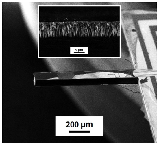
Figure 6.
Inclined-view SEM graph of a Si microcantilever with ZnO NRs grown on its back surface (inset).
4. Conclusions
In this work, a DC-sputtered/annealed ZnO seed-layer and chemical-bath deposition based two-step ZnO NRs arrays growth method was introduced, and ZnO NRs arrays grown on seed-layers annealed under different temperatures were characterized to study their area density, diameter, crystallinity and resistivity. The SEM graphs, XRD patterns and four-point probe resistivity measurements illustrate that NRs arrays grown on the seed-layer annealed at 600 °C have the best c-axis orientation and vertical alignment as well as the highest surface-area enlargement factor of 48 (with 6 µm in length). Next, further properties relevant for MEMS devices applications, e.g., growth of NRs on different materials, vacancy concentrations and optical properties will be investigated.
Author Contributions
J.X. and E.P. conceived and designed the experiments; J.X. and A.S. performed the experiments; K.S., H.Z. and M.B. analyzed the data; A.W. and E.P. contributed reagents/materials/analysis tools; J.X. wrote the paper, E.P. revised the paper, A.W. and E.P. supervised the research.
Acknowledgments
Juliane Breitfelder, and Karl-Heinz Lachmund provided valuable technical support, J.X. is grateful for funding by the China Scholarship Council (CSC) under the Grant CSC No. 201506300019. Furthermore, we acknowledge the support from “Niedersachsisches Vorab”, Germany, through the “Quantum- and anometrology (QUANOMET)” initiative within the project of “NP 2-2 and from the German research Foundation (DFG) under no. PE 885/3-1.
Conflicts of Interest
The authors declare no conflict of interest.
References
- Bakin, A.; Behrends, A.; Wagner, A.; Waag, A. Fabrication of ZnO Nanostructures. In Zinc Oxide Nanostructures; Pan Stanford Publishing Pte Ltd.: Singapore, 2014; ISBN 978-981-4411-33-2. [Google Scholar]
- Liu, S.Y.; Chen, T.; Wan, J.; Ru, G.P.; Li, B.Z.; Qu, X.P. The effect of pre-annealing of sputtered ZnO seed layers on growth of ZnO nanorods through a hydrothermal method. Appl. Phys. A 2009, 94, 775–780. [Google Scholar] [CrossRef]
- Xu, J.; Bertke, M.; Li, X.; Mu, H.; Zhou, H.; Yu, F.; Hamdana, G.; Schmidt, A.; Bremers, H.; Peiner, E. Fabrication of ZnO nanorods and Chitosan@ZnO nanorods on MEMS piezoresistive self-actuating silicon microcantilever for humidity sensing. Sens. Actuators B Chem. 2018, 273, 276–287. [Google Scholar] [CrossRef]
- Xu, J.; Bertke, M.; Gad, A.; Yu, F.; Hamdana, G.; Bakin, A.; Peiner, E. Fabrication of ZnOnanorods on MEMS piezoresistive silicon microcantilevers for environmental monitoring. Proceedings 2017, 1, 290. [Google Scholar]
- Huang, J.S.; Lin, C.F. Influences of ZnO sol-gel thin film characteristics on ZnO nanowire arrays prepared at low temperature using all solution-based processing. J. Appl. Phys. 2008, 103, 014304. [Google Scholar] [CrossRef]
- Xu, J.; Bertke, M.; Li, X.; Mu, H.; Peiner, E. Self-actuating and self-sensing ZNO nanorods/chitosan coated piezoresistive silicon microcantilever for humidity sensing. In Proceedings of the 2008 IEEE Micro Electro Mechanical Systems (MEMS), Belfast, UK; 2018; pp. 206–209. [Google Scholar]


Publisher’s Note: MDPI stays neutral with regard to jurisdictional claims in published maps and institutional affiliations. |
© 2018 by the authors. Licensee MDPI, Basel, Switzerland. This article is an open access article distributed under the terms and conditions of the Creative Commons Attribution (CC BY) license (https://creativecommons.org/licenses/by/4.0/).