Area-Selective Growth of Aligned ZnO Nanorod Arrays for MEMS Device Applications †

 ,
, 
Abstract
:1. Introduction
2. Experimental
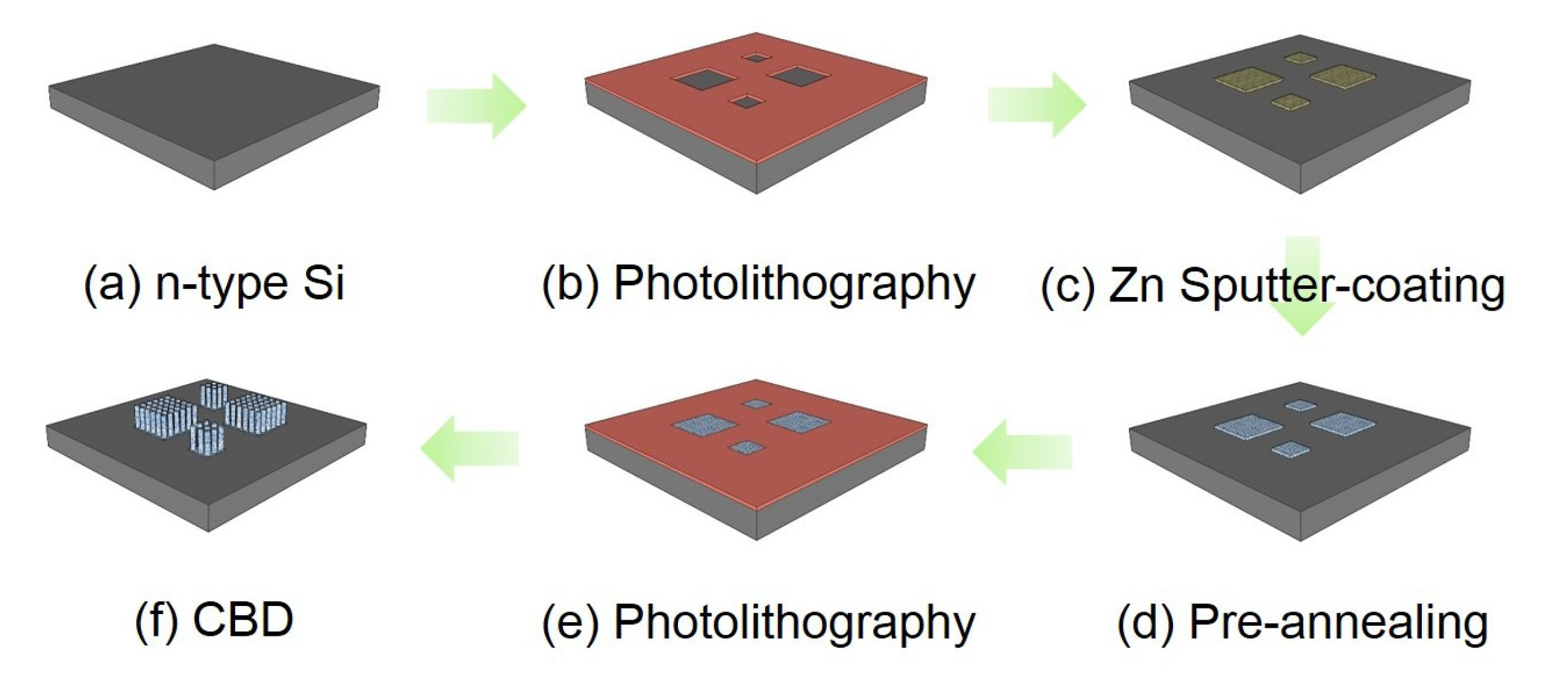
Area-Selective Growth of Aligned ZnO Nanorods Arrays
- (a)
- The fabrication started from a piece of sample with a dimension of 30 × 30 mm2, the sample was cut from an n-type bulk-silicon wafer (crystal orientation: <100>; resistivity: 1–10 Ω × cm; thickness: 275 ± 15 µm and diameter: 100 ± 0.13 mm) and cleaned by putting the sample into a boiling acid mixture (H2O2 (30%) and H2SO4 (96%), v:v = 1:1) for 5 min.
- (b)
- A positive photoresist (AZ 5214E, Merck, Kenilworth, NJ, USA) was utilized during the subsequent photolithography step and a MJB4 mask aligner (SÜSS MicroTec AG, Garching, Germany) was used to expose the pattern area. Prior to the exposure, the photoresist spin-coating procedure was run at a speed of 5000 rpm for 35 s, to create a homogenous photoresist layer of 1.5 µm in thickness. After the exposure, the sample was then dipped and developed in AZ 726 MIF developer solution (MicroChemicals, Merck) for 60 s, followed by DI water rinsing and nitrogen purging.
- (c)
- Afterwards, a polycrystalline Zn film was prepared by sputtering Zn (99.99%) using high purity Ar (99.99%) gas under 50 µA direct current (DC), at room temperature (25 °C) and a working pressure of 640 Pa. To obtain the selective deposition of sputtering film on the patterned area, the excess ZnO was removed using photoresist lift-off.
- (d)
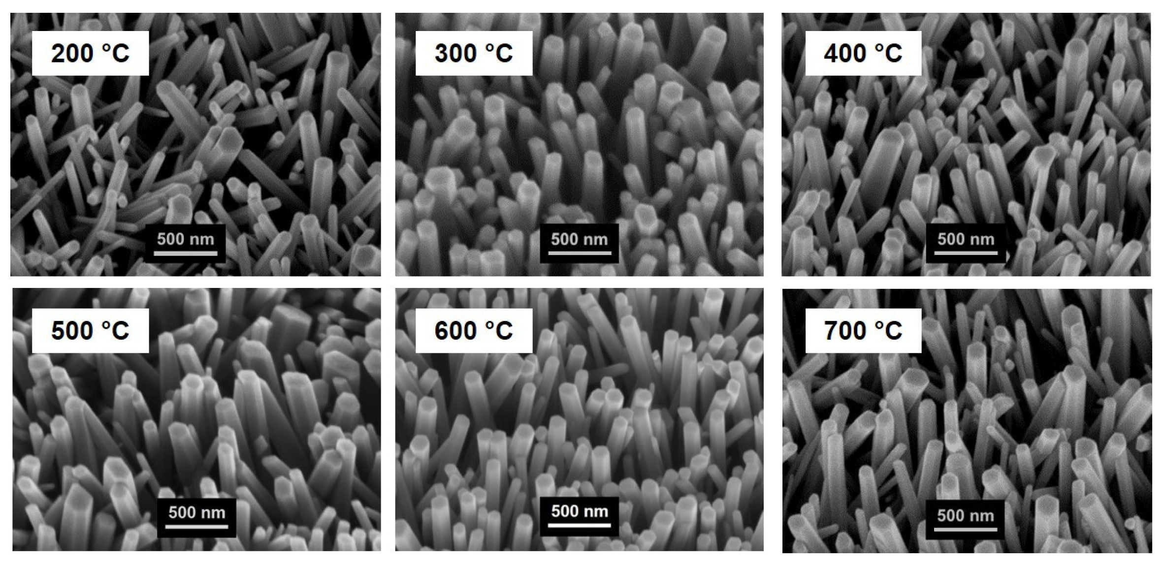
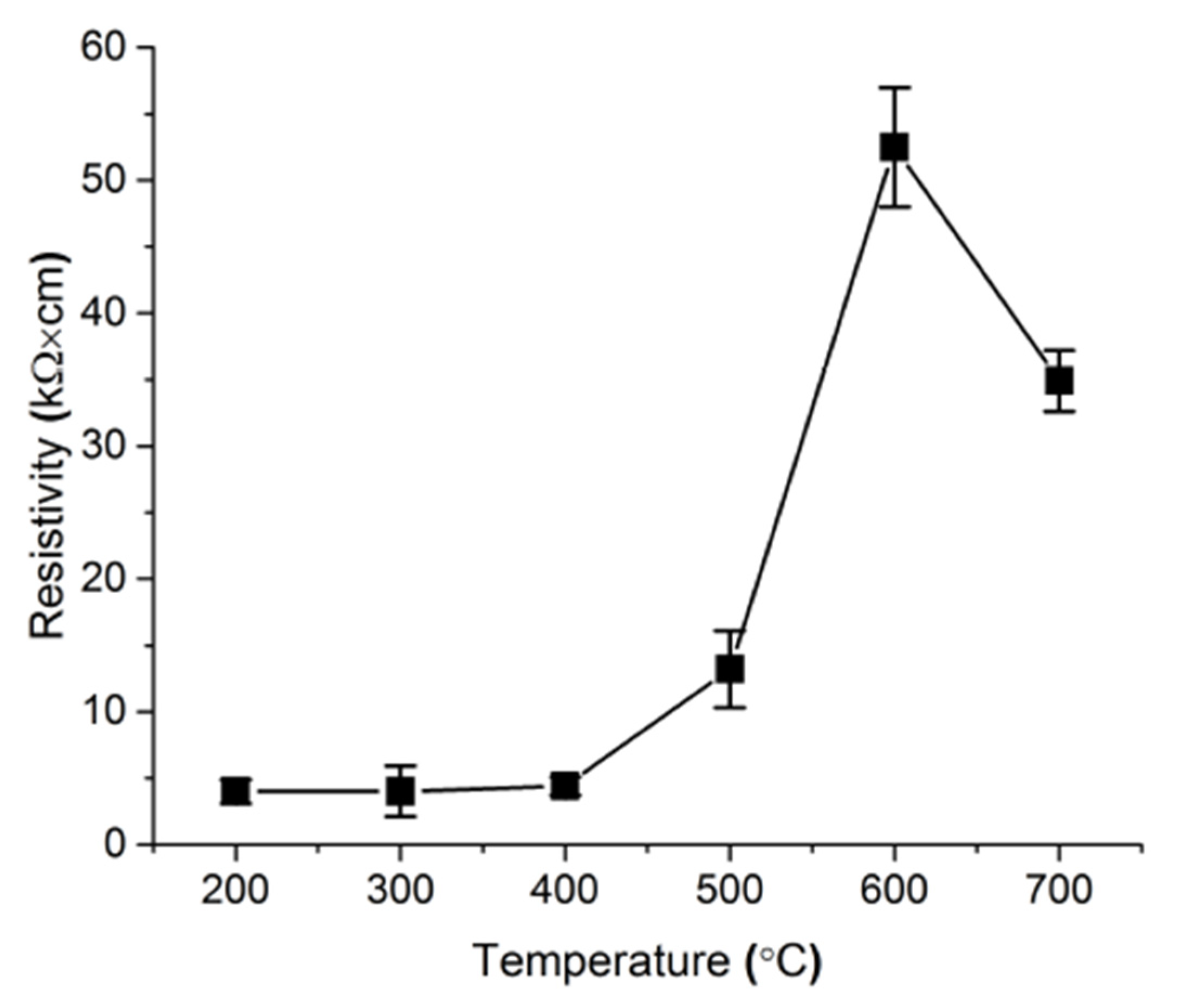
- Then the sputtered Zn-film was annealed in an oven with open atmosphere, to investigate influence of annealing temperature on the nanorods growth, the sputtered samples were annealed at 200 °C, 300 °C, 400 °C, 500 °C, 600 °C and 700 °C, respectively.
- (e)
- When the seed-layer has been prepared, a subsequent photolithography step was implemented corresponding to step (b) to protect the substrate during the next CBD process.
- (f)
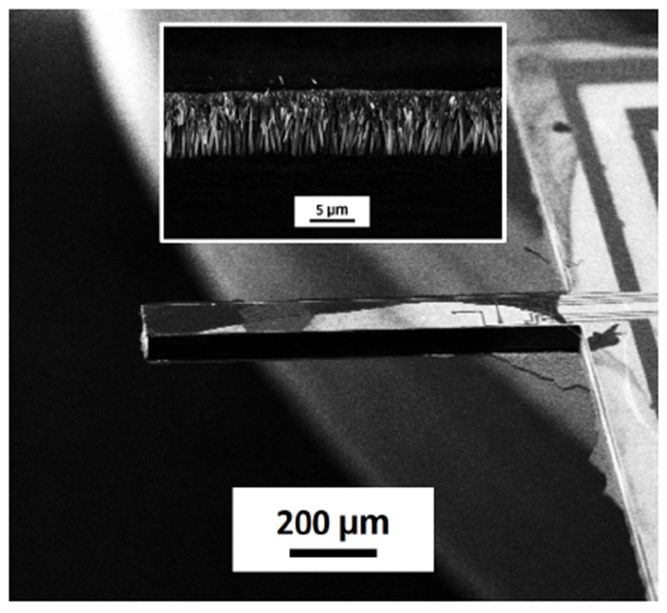
- ZONRs were grown by dipping the sample in an aqueous solution, which consisted of 30 mmol/L zinc nitrate (Zn(NO3)2) and 30 mmol/L hexamethyleneteramine (HMT, C6H12N4), respectively. The deposition was carried out in a temperature-controlled chemical reactor, which was additionally equipped with a thermometer and a reflux condenser, for 3 h at 90 °C. After the reaction, the sample was cleaned with acetone and deionized water, successively [4].
3. Results and Discussion
4. Conclusions
Author Contributions
Acknowledgments
Conflicts of Interest
References
- Bakin, A.; Behrends, A.; Wagner, A.; Waag, A. Fabrication of ZnO Nanostructures. In Zinc Oxide Nanostructures; Pan Stanford Publishing Pte Ltd.: Singapore, 2014; ISBN 978-981-4411-33-2. [Google Scholar]
- Liu, S.Y.; Chen, T.; Wan, J.; Ru, G.P.; Li, B.Z.; Qu, X.P. The effect of pre-annealing of sputtered ZnO seed layers on growth of ZnO nanorods through a hydrothermal method. Appl. Phys. A 2009, 94, 775–780. [Google Scholar] [CrossRef]
- Xu, J.; Bertke, M.; Li, X.; Mu, H.; Zhou, H.; Yu, F.; Hamdana, G.; Schmidt, A.; Bremers, H.; Peiner, E. Fabrication of ZnO nanorods and Chitosan@ZnO nanorods on MEMS piezoresistive self-actuating silicon microcantilever for humidity sensing. Sens. Actuators B Chem. 2018, 273, 276–287. [Google Scholar] [CrossRef]
- Xu, J.; Bertke, M.; Gad, A.; Yu, F.; Hamdana, G.; Bakin, A.; Peiner, E. Fabrication of ZnOnanorods on MEMS piezoresistive silicon microcantilevers for environmental monitoring. Proceedings 2017, 1, 290. [Google Scholar]
- Huang, J.S.; Lin, C.F. Influences of ZnO sol-gel thin film characteristics on ZnO nanowire arrays prepared at low temperature using all solution-based processing. J. Appl. Phys. 2008, 103, 014304. [Google Scholar] [CrossRef]
- Xu, J.; Bertke, M.; Li, X.; Mu, H.; Peiner, E. Self-actuating and self-sensing ZNO nanorods/chitosan coated piezoresistive silicon microcantilever for humidity sensing. In Proceedings of the 2008 IEEE Micro Electro Mechanical Systems (MEMS), Belfast, UK; 2018; pp. 206–209. [Google Scholar]


| 200 °C | 300 °C | 400 °C | 500 °C | 600 °C | 700 °C | |
|---|---|---|---|---|---|---|
| Diameter (nm) | 60 ± 20 | 87 ± 27 | 66 ± 24 | 99 ± 31 | 93 ± 24 | 74 ± 26 |
| Area density (μm−2) | 25 ± 5 | 21 ± 1 | 27 ± 2 | 21 ± 5 | 27 ± 2 | 17 ± 4 |
Publisher’s Note: MDPI stays neutral with regard to jurisdictional claims in published maps and institutional affiliations. |
© 2018 by the authors. Licensee MDPI, Basel, Switzerland. This article is an open access article distributed under the terms and conditions of the Creative Commons Attribution (CC BY) license (https://creativecommons.org/licenses/by/4.0/).
Share and Cite
Xu, J.; Strempel, K.; Zhou, H.; Waag, A.; Bertke, M.; Schmidt, A.; Peiner, E. Area-Selective Growth of Aligned ZnO Nanorod Arrays for MEMS Device Applications. Proceedings 2018, 2, 887. https://doi.org/10.3390/proceedings2130887
Xu J, Strempel K, Zhou H, Waag A, Bertke M, Schmidt A, Peiner E. Area-Selective Growth of Aligned ZnO Nanorod Arrays for MEMS Device Applications. Proceedings. 2018; 2(13):887. https://doi.org/10.3390/proceedings2130887
Chicago/Turabian StyleXu, Jiushuai, Klass Strempel, Hao Zhou, Andreas Waag, Maik Bertke, Angelika Schmidt, and Erwin Peiner. 2018. "Area-Selective Growth of Aligned ZnO Nanorod Arrays for MEMS Device Applications" Proceedings 2, no. 13: 887. https://doi.org/10.3390/proceedings2130887