2. Materials and Methods
One type of PIN photodiodes [
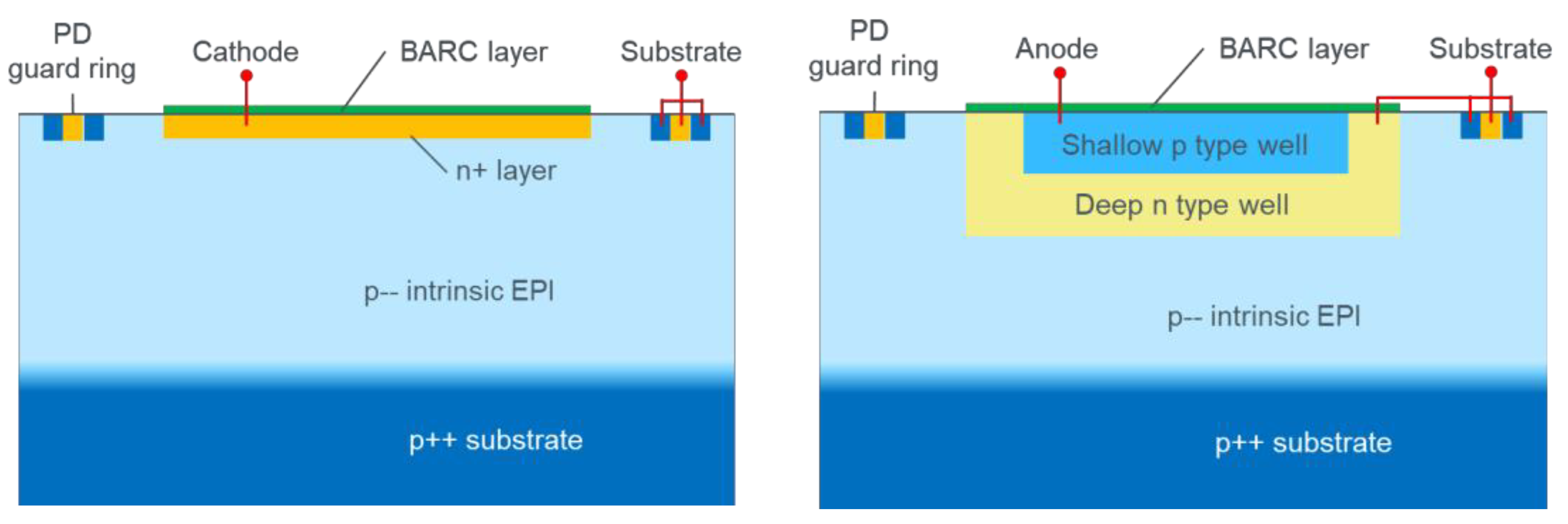
2] is constructed with a shallow highly doped n+ type well in intrinsic p-type EPI (iEPI) (
Figure 1a), hereafter called nPD. Another type optimized for blue wavelengths uses deep n-type well with a counter-doped shallow p-type well, thus making the photodiode less sensible to red and near infrared wavelengths (
Figure 1b), hereafter called bluePD. By shortening deep n-type well and substrate, the photocurrent generated in the iEPI recombines and does not contribute to the photocurrent collected by the shallow p-well layer.
All photodiodes have been processed in an industry standard 350 nm high-voltage CMOS technology. The photodiodes’ layout permits a direct pad access to anodes and cathodes without any signal amplification circuit. Photodiodes’ optical characteristics are measured by guiding light from a tunable light source operating from 400 nm to 900 nm wavelengths through a multimode fiber placed above the photodiodes and measuring generated photocurrent on the different pads.
3. Results
Figure 2a presents the impact of the iEPI layer thicknesses and the BARC layers thicknesses on spectral responsivity (SR) for circular and square nPDs. Larger iEPI thickness increases the spectral response in near infrared wavelengths reaching a responsivity of 0.63 A/W at 800 nm for a 30 µm iEPI thickness while the BARC layer increases the local spectral response at its optimized wavelength. The spectral responsivity reaches 100% of the quantum efficiency for BARC layers optimized for λ = 750 nm and λ = 900 nm and 82% for layer optimized for λ = 425 nm wavelengths.
The leakage current of circular nPD (
Figure 2b and
Figure 3a,b) is dependent on iEPI thickness, doping concentration, and the distance of photodiode to the guard ring [
3]. The increase of the iEPI thickness increases the space charge region width around the pn junction thus increases the leakage current. The extension of the space charge region is more pronounced when the doping concentration of the EPI is closer to the intrinsic concentration ni which is confirmed by TCAD simulations shown in
Figure 3a. At high bias voltage, we can see an increase of the leakage current due to the proximity of the photodiode guard ring consisting of a pnp substrate contact configuration where the n type contact layer is used for the reduction of photodiode to photodiode electrical and optical crosstalk. This configuration generates a lateral npn bipolar with the photodiode which increases the leakage current of the photodiode. In
Figure 3b, we can observe that the leakage current is linearly dependent on the photodiode diameter or perimeter.
The capacitance of the circular nPD is also dependent on the iEPI thickness and photodiode size (
Figure 4a,b). The nPD capacitance is bounded by the iEPI thickness because of the low resistive substrate placed below the iEPI layer that is blocking the extension of the space charge width in depth of the photodiode. The circular photodiodes capacitance is linearly dependent to the surface of the photodiode while the impact of the BARC is limited (
Figure 4b).
In addition to circular PIN photodiodes, square PIN photodiodes with a fixed single photodiode geometry of 200 µm × 200 µm are placed. We also processed arrays of 16 square photodiodes (4 × 4, each 200 µm × 200 µm), 49 square photodiodes (7 × 7) and 121 square photodiodes (11 × 11). The cathodes of all the photodiodes placed in an array are connected together. For arrays, the pnp guard ring is only placed around the array while each blocks have only a p type substrate contact.
Figure 5a shows the capacitance of a single square photodiode with 20 µm and 30 µm iEPI thicknesses. As observed for circular photodiodes, the capacitance is lowered when the iEPI thickness is increased. However, because of the smaller size of the squared photodiode, the space charge region of the photodiode reaches the n contact of the guard ring and thus limits the capacitance of the photodiode between 0 V and −1.5 V for 30 µm iEPI. This limitation is not observed for arrays.
Figure 5b shows the evolution of the capacitance of the square PIN photodiode versus the number of photodiodes placed in an array. The capacitance is varying linearly to the number of block. As each block has a fixed geometry, the capacitance is varying linearly to the surface of the array.
In the case of optimized bluePD (
Figure 1b), the impact of iEPI thickness on the spectral responsivity curve is limited due to the internal collection of photocurrent while the application of a BARC layer optimized at λ = 425 nm increases the spectral current collected for short wavelengths (
Figure 6a). Because of the internal structure of the bluePD, the leakage current is not dependent on the iEPI thickness and is around 10 pA at a biasing below −1 V for a 150 µm × 150 µm photodiode size designed in a square configuration (
Figure 6b).
