Abstract
A self-standing porous silicon (PS) multilayer structure detached from the substrate by the lift-off method and integrated with a microfluidic cell is presented. Experiments of refractive index changes sensing flow through open-ended pores are reported. We continuously recorded the reflectance spectra of the PS membrane each 30 s and measured the shift as different substances flowed through the structure. The experimental sensitivity values are in good agreement with the theoretical simulations performed.
1. Introduction
Porous silicon (PS) [1] is a good host for the fabrication of high-sensitivity optical sensors. Its sponge-like structure is very sensitive to changes in the refractive index of the medium filling the pores or the adsorption of analytes on its surface. A high aspect ratio between the surface and volume can be achieved [2], which results in a high sensitivity, allowing the miniaturization of the sensor and the reduction of the limit of detection.
The formation of PS occurs under the anodization of silicon in hydrofluoric acid (HF) solutions, known as electrochemical etching [3]. Etching conditions, such as the anodization current or solution composition, define the porosity of the PS layer. Likewise, the etching time determines its thickness. The pore size also can be tuned from less than 5 nm (micropores) to more than 1 μm (macropores) [4]. However, the highest sensitivity is reached for small pore sizes [5].
P-type silicon wafers have some advantages concerning PS formation, e.g., better surface and vertical uniformity [6], linear etching rates [7,8], and a lack of need for backside illumination [9]. For heavily doped p-type silicon, micropores are formed with most HF solutions [4]. However, certain applications in which pore walls will be biofunctionalized [10,11] or some molecules must penetrate the pores [12] require a bigger pore diameter. For this purpose, some organic solvents, such as dimethylformamide (DMF), are combined with HF to increase pore size during anodization [13,14].
Close-ended PS structures used for sensing purposes, e.g., Fabry–Pèrot interferometers [15] and distributed Bragg reflectors [16], have reported good results. Nonetheless, they may suffer some effects such as air entrapment and bad flow diffusion that can lower the sensitivity and reduce the sensor performance [17,18]. It has been demonstrated that flowing through open-ended PS films reduces the time of detection, optimizes the sensitivity, and avoids the mixture of different substances [19]. There are several methods for obtaining open-ended pores, but lift-off is the easiest and fastest method [20]. In this method, the PS structure is detached from the substrate in a single step by electrochemically etching with a current close to electropolishing. The self-standing PS membrane can be integrated in a microfluidic cell in order to perform sensing experiments.
2. Methods
PS was prepared by electrochemically etching highly doped p-type silicon (boron doped, <100> oriented, 0.01–0.02 Ω∙cm resistivity) purchased from MicroChemicals GmbH (Ulm, Germany). Ethanol (EtOH) and 2-propanol (IPA) were obtained from Scharlab S.L. (Barcelona, Spain) and N,N-dimethylformamide (DMF) was obtained from Sigma-Aldrich (Saint Louis, MO, USA). Hydrofluoric acid (HF) (48% solution in water), hydrogen peroxide (H2O2), and sulfuric acid (H2SO4) were purchased from BASF (Ludwigshafen am Rhein, Germany). Deionized water (DIW) was produced in house by a Millipore water purification system.
All silicon samples were pretreated for 30 min in a 3:1 volumetric mixture of H2SO4 and H2O2 for cleaning organic residues off the substrate. Afterward, they were dipped into a solution of <5% HF for 30 s to remove the native oxide layer.
PS films were fabricated under galvanostatic conditions with a Pt electrode using an electrolyte solution of HF:DIW:DMF in a 1:1:4 volumetric ratio (see electrochemical cell in Figure 1a). Multilayer alternating regions of high (H) and low (L) porosity were formed using anodization current densities of 22 mA/cm2 (82% porosity) and 8 mA/cm2 (62% porosity), respectively. The etching times were 27.5 s and 24 s for H and L layers to have a photonic bandgap (PBG) in the visible region of the spectrum.
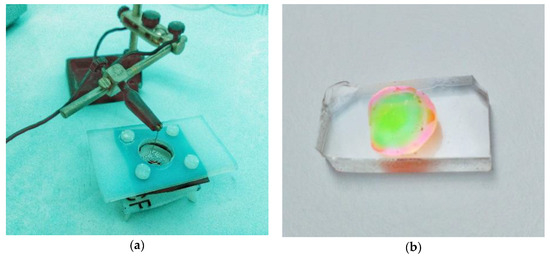
Figure 1.
(a) Electrochemical cell used in this work for fabricating porous silicon (PS) samples; (b) PS multilayer detached from the substrate.
After the formation of eight periods of H and L layers, an anodization current of 45 mA/cm2, close to electropolishing, was applied to allow the later lift-off of PS film from the substrate. Then, samples were oxidized in an oven at 800 °C for 15 min in an oxygen atmosphere. Figure 1b shows an example of what the PS multilayer looks like after detachment.
A microfluidic flow cell was designed to facilitate the ability of the PS film to sense materials flowing over and through the pores. First, membranes were detached from the substrate using a polydimethylsiloxane (PDMS) layer with holes for the tubes already assembled. A microchannel was then attached between the PS film and a glass slide. Together, this cell forced the liquids to pass from the inlet tube through the pores to the microchannel and again through the PS film to the outlet tube.
All measurements were performed using a Fourier transform infrared spectroscope (FTIR) (Bruker, Billerica, MA, USA) in the range between 500 and 910 nm. Reflectance spectra of the PS film were collected every 30 s with an acquisition time of 20 s. For the experiments, three different liquids were directed through the flow cell, i.e., DIW, EtOH, and IPA. Recorded data were processed with a MATLAB (vR2016b) program and the shift of the local maximum was measured at approximately 850 nm. Sensitivity, described as the spectral shift divided by the refractive index increase, was calculated considering the refractive indices of DIW, EtOH, and IPA, which were 1.329 [21], 1.3555, and 1.3718 [22], respectively.
3. Results and Discussion
A simulation program based on the Transfer Matrix Method (TMM) [23] was used to compare the theoretical response of the sensor with the experimental results of the fabricated PS film. Figure 2a shows the simulated reflectance spectra of a multilayer of eight periods with 82% and 62% of porosity in each layer and thicknesses of 320 nm and 240 nm, for different media filling the pores, i.e., DIW, EtOH, and IPA. Figure 2c shows the local maximum position for each substance, which led to a theoretical sensitivity of this structure of 358.6 nm/RIU (refractive index unit).
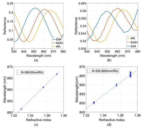
Figure 2.
(a) Simulated reflectance spectra of the sensor for different media filling the pores; (b) experimental reflectance spectra of the fabricated sensor; (c) theoretical local maximum position and sensitivity; (d) measured local maximum position and experimental sensitivity.
Figure 2b shows the reflectance spectra registered with FTIR for the fabricated PS sample while different substances were directed to flow through the pores. Only a group of three are represented for purposes of clarity. The position of the local maximum for all recorded data during the experiment is represented in Figure 2d. An experimental sensitivity of 355.9 nm/RIU was achieved. Therefore, the experimental results are in perfect agreement with the simulations.
4. Conclusions
In this work, we presented the fabrication of a PS membrane detached from the substrate by the lift-off method and demonstrated its use as a sensor for the detection of refractive index changes. Allowing flow through open-ended pores optimizes the sensitivity and allows the full design value to be reached. A sensitivity of 355.9 nm/RIU was achieved in the visible range of the spectrum.
Funding
The authors acknowledge the funding from the Spanish government through the project TEC2015-63838-C3-1-R-OPTONANOSENS.
References
- Pacholski, C. Photonic crystal sensors based on porous silicon. Sensors 2013, 13, 4697–4713. [Google Scholar] [CrossRef] [PubMed]
- Bisi, O.; Ossicini, S.; Pavesi, L. Porous silicon: A quantum sponge structure for silicon based optoelectronics. Surf. Sci. Rep. 2000, 38, 6–21. [Google Scholar] [CrossRef]
- Kolasinski, K.W. Etching of silicon in fluoride solutions. Surf. Sci. 2009, 603, 1904–1911. [Google Scholar] [CrossRef]
- Zhang, G.X. Porous silicon: Morphology and formation mechanisms. In Modern Aspects of Electrochemistry; Vayenas, C., Gamboa-Adelco, M.E., Eds.; Springer: Boston, MA, USA, 2006; Volume 39, pp. 65–133. ISBN 0076-9924. [Google Scholar]
- Suárez, I.; Chirvony, V.; Hill, D.; Martínez-Pastor, J. Simulation of surface-modified porous silicon photonic crystals for biosensing applications. Photonic Nanostructures Fundam. Appl. 2012, 10, 304–311. [Google Scholar] [CrossRef]
- Agarwal, V. Porous silicon multilayers and superlattices. In Handbook of Porous Silicon; Canham, L.T., Ed.; Springer International Publishing: Geneva, Switzerland, 2014; pp. 153–162. ISBN 978-3-319-05744-6. [Google Scholar]
- Halimaoui, A. Porous silicon formatin by anodization. In Properties of Porous Silicon; Canham, L.T., Ed.; IEEE INSPEC: London, UK, 1997; Volume 12, ISBN 0852969325. [Google Scholar]
- Frohnhoff, S.; Berger, M.G.; Thönissen, M.; Arens-Fischer, R.; Munder, H.; Lüth, H.; Arntzen, M.; Thei, W. Formation techniques for porous silicon superlattices. Thin Solid Films 1995, 255, 59–62. [Google Scholar] [CrossRef]
- Föll, H.; Christophersen, M.; Carstensen, J.; Hasse, G. Formation and application of porous silicon. Mater. Sci. Eng. R. 2002, 39, 93–141. [Google Scholar] [CrossRef]
- Mariani, S.; Strambini, L.M.; Barillaro, G. Femtomole detection of proteins using a label-free nanostructured porous silicon interferometer for perspective ultrasensitive biosensing. Anal. Chem. 2016, 88, 8502–8509. [Google Scholar] [CrossRef] [PubMed]
- Arroyo-Hernández, M.; Martín-Palma, R.J.; Pérez-Rigueiro, J.; García-Ruiz, J.P.; García-Fierro, J.L.; Martínez-Duart, J.M. Biofunctionalization of surfaces of nanostructured porous silicon. Mater. Sci. Eng. C 2003, 23, 697–701. [Google Scholar] [CrossRef]
- Karlsson, L.M.; Tengvall, P.; Lundström, I.; Arwin, H. Penetration and loading of human serum albumin in porous silicon layers with different pore sizes and thicknesses. J. Colloid Interface Sci. 2003, 266, 40–47. [Google Scholar] [CrossRef] [PubMed]
- Lehmann, V.; Stengl, R.; Luigart, A. On the morphology and the electrochemical formation mechanism of mesoporous silicon. Mater. Sci. Eng. B 2000, 69–70, 11–22. [Google Scholar] [CrossRef]
- Haldar, S.; De. A.; Chakraborty, S.; Ghosh, S.; Ghanta, U. Effect of dimethylformamide, current density and resistivity on pore geometry in p-type macroporous silicon. Procedia Mater. Sci. 2014, 5, 764–771. [Google Scholar] [CrossRef]
- Hutter, T.; Horesh, M.; Ruschin, S. Method for increasing reliability in gas detection based on indicator gradient in a sensor array. Sens. Actuators B 2011, 152, 29–36. [Google Scholar] [CrossRef]
- Kovacs, A.; Malisauskaite, A.; Ivanov, A.; Mescheder, U.; Wittig, R. Optical sensing and analysis system based on porous layers. In Proceedings of the 17th International Conference on Miniaturized Systems for Chemistry and Life Sciences, Freiburg, Germany, 27–31 October 2013; pp. 275–277. [Google Scholar]
- Zhao, Y.; Gaur, G.; Mernaugh, R.L.; Laibinis, P.E.; Weiss, S.M. Comparative kinetic analysis of closed-ended and open-ended porous sensors. Nanoscale Res. Lett. 2016, 11, 395. [Google Scholar] [CrossRef] [PubMed]
- Kumar, N.; Froner, E.; Guider, R.; Scarpa, M.; Bettotti, P. Investigation of non-specific signals in nanoporous flow-through and flow-over based sensors. Analyst 2014, 139, 1345–1349. [Google Scholar] [CrossRef] [PubMed]
- Zhao, Y.; Gaur, G.; Retterer, S.T.; Laibinis, P.E.; Weiss, S.M. Flow-through porous silicon membranes for real-time lable-free biosensing. Anal. Chem. 2016, 88, 10940–10948. [Google Scholar] [CrossRef] [PubMed]
- Solanki, C.S.; Bilyalov, R.R.; Poortmans, J.; Celis, J.P.; Nijs, J.; Mertens, R. Self-standing porous silicon films by one-step anodizing. J. Electrochem. Soc. 2004, 151, C307–C314. [Google Scholar] [CrossRef]
- Hale, G.M.; Querry, M.R. Optical constants of water in the 200-nm to 200-μm wavelength region. App. Opt. 1973, 12, 555–563. [Google Scholar] [CrossRef] [PubMed]
- Sani, E.; Dell’Oro, A. Spectral optical constants of ethanol and isopropanol from ultraviolet to far infrared. Opt. Mater. 2016, 60, 137–141. [Google Scholar] [CrossRef]
- Balili, R.B. Transfer matrix method in nanophotonics. Int. J. Mod. Phys. 2012, 17, 159–168. [Google Scholar] [CrossRef]

© 2018 by the authors. Licensee MDPI, Basel, Switzerland. This article is an open access article distributed under the terms and conditions of the Creative Commons Attribution (CC BY) license (https://creativecommons.org/licenses/by/4.0/).