Article

On the Processability and Microstructural Evolution of CuCrZr in Multilayer Laser-Directed Energy Deposition Additive Manufacturing via Statistical and Experimental Methods

1
Multi-Scale Additive Manufacturing Lab, Department of Mechanical and Mechatronics Engineering, University of Waterloo, Waterloo, ON N2L 3G1, Canada
2
Fatigue and Stress Analysis Laboratory (FATSLab), Department of Mechanical & Mechatronics Engineering, University of Waterloo, 200 University Avenue West, Waterloo, ON N2L 3G1, Canada
*
Author to whom correspondence should be addressed.
J. Manuf. Mater. Process. 2023, 7(4), 151; https://doi.org/10.3390/jmmp7040151
Submission received: 9 July 2023 / Revised: 15 August 2023 / Accepted: 16 August 2023 / Published: 18 August 2023
(This article belongs to the Special Issue Advances in Metal Additive Manufacturing/3D Printing)

Abstract

:
Laser-directed energy deposition (LDED) is a promising technology for coating, repairing, and building near-net-shape 3D structures. However, the processing of copper alloys, specifically, has presented a significant challenge due to their low laser absorptivity at the 1060 nm laser wavelength and high thermal conductivity. This study undertook a methodical examination by employing a 2 kW disk laser, operating at a wavelength of 1064 nm, and a coaxial nozzle head to comprehensively examine the processability of the highly conductive CuCrZr alloy for expanding the range of materials that can be successfully processed using LDED. The investigation focuses not only on optimizing the input process parameters that are the laser power, scanning speed, powder feed rate, and overlap ratio, but also on planning the toolpath trajectory, as these factors were found to exert a substantial influence on processability, geometrical accuracy, and the occurrence of defects such as lack of fusion. The optimal toolpath trajectory discovered involved implementing a zigzag strategy combined with a 90° rotation of the scanning direction. Additionally, a start point rotation was considered between each layer to even out the deposition of the layers. Moreover, a contour with a radial path at the corners was introduced to enhance the overall trajectory. Based on the hierarchal experimental study, the appropriate ranges for the key process parameters that leads to 99.99% relative density have been identified. They were found to be from 1100 up to 2000 W for the laser power (P), and from 0.003 up to 0.016 g/mm for the amount of powder that is fed to the melt pool distance (F/V). Regarding the influence of process parameters on the microstructure of the samples with equal deposition height, it was observed that varying combinations of process parameters within the optimal processing window resulted in variations in grain size ranging from 105 to 215 µm.

1. Introduction

Laser-directed energy deposition (LDED) is an additive manufacturing (AM) method where material (powder/wire) is fed into a focused laser beam and deposited onto pre-existing layers [1]. This approach provides a notable advantage over other AM methods as it is less constrained by part size. Therefore, it presents a promising option for the production of sizable aerospace components that are frequently subjected to extreme environments encompassing elevated temperatures, high-pressure static loads, thermo-mechanical stresses, fatigue, and intense dynamic loading [2,3,4]. However, integrating LDED parts into critical components that undergo complex mechanical and thermal loads necessitates precise optimization of process parameters to avoid defects in both macro and micro scales. Macro-scale defects are mainly attributed to geometrical inaccuracies in the deposition. During the LDED process, non-uniformity and severe deformation often occur in the multi-layer deposition, which further affects the overall geometrical accuracy of fabricated parts. The dimensional accuracy of fabricated parts is critically influenced by the process parameters, the overlap ratio of adjacent tracks, and toolpath trajectory [4,5].
On the other hand, microscopic defects are mainly formed in the finished part during the laser–powder–metal interaction and determine the macroscopic response of the part to external loading and environmental factors [1,6,7]. Overall, four different types of defects are observed in LDED, namely, lack-of-fusion porosity (LOF), keyhole porosity, balling, and gas porosity [8]. In more detail, the lack-of-fusion porosity boundary can be determined by whether there is sufficient overlap between melt pools to ensure that all points are melted at least once [9]. On the contrary, the presence of keyhole porosity indicates an excessive amount of energy density being applied to the fed powder/substrate materials. This excessive energy leads to vaporization, instabilities in the melt pool, and the formation of pores that eventually close off [10]. The balling defect is the formation of a ball of material on top of the substrate or previous layer due to poor wetting [11,12]. Entrapped gas in powder particles and/or meltpool is another common source of porosity in LDED products that release during laser–material interaction and entraps again due to the fast solidification of molten material [13]. In order to limit defect formation within fabricated parts and maintain geometrical accuracy, the tool path trajectory and main process parameters which are laser power, scanning speed, powder feed rate, and overlap ratio must be optimized concurrently [14,15].
Copper-based alloys have been the preferred choice of material for high-heat flux applications such as the aerospace industry and nuclear fusion sector [16,17]. Among Cu alloys, the CuCrZr offers an appropriate balance of thermal conductivity and mechanical strength that make it an interesting option [18,19]. Moreover, the ability to quickly produce complex geometries has made AM a strong candidate for manufacturing such parts made of CuCrZr alloy. In that regard, several works have been reported on AM of CuCrZr alloy, mostly on the manufacturing matters and the effect of process parameters on the microstructure and mechanical properties.
A comparative investigation by Lassègue et al. [20] conducted on the laser powder bed fusion (LPBF) of Cu, Cu+CrZr (coated), and CuCrZr alloy powders addressed the difficulties associated with achieving full density using commercial lasers like fiber (5.6%), CO2 (26%), and YAG (39–59%) lasers [7,21], owing to their high thermal conductivity and the limited energy absorption capacity. Guan et al. [19] explored the impact of various process parameters and heat treatments on the mechanical strength and electrical conductivity of CuCrZr fabricated through LPBF. They successfully enhanced the relative density to approximately 97%, achieving a strength of up to 267 MPa. The researchers observed that elevating the aging temperature led to improved electrical conductivity; however, this increase in conductivity was accompanied by a significant reduction in strength, likely attributable to excessive precipitation. There is only one work carried out by Ordas et al. [22] on electron beam powder bed fusion of CuCrZr. Due to the nature of this technique, processing CuCrZr alloy is less challenging, and issues associated with high thermal conductivity, high reflectivity, and oxidation are prevented. In their work, a processing window that leads to a nearly fully dense part (99.8%) was identified, and microstructural evolution, as well as thermal conductivity and hardness, have been correlated with the main process parameters and post-build ageing.
Yet, the aerospace industry often requires the manufacturing of large components, some of which exceed 0.5 m in size and operate in extreme environments involving high temperatures, high-pressure static loads, thermo-mechanical, fatigue, and high dynamic loading. To address this requirement, LDED stands as the sole choice among AM techniques that has been reported the production of sizeable components with intricate geometries, specifically utilizing the CuCrZr alloy [23,24,25]. Zardoshtian et al. [26] conducted a study on LDED processing of CuCrZr alloy in the single-track scale. First, they optimized the main process parameters using a two-step statistical approach and multiple DOEs. From the microstructural characterization, the Cr particles were observed in the copper matrix, which was in the form of a cellular solidification structure. Further, they studied the effect of process parameters on the microstructural evolution, mainly on morphology and the average size of the grain structure. The maximum columnarity of grain morphology was seen in the sample with maximum laser power and minimum fed powder per distance. They showed that the top region of deposition has higher hardness (up to 110 HV) than near the melt pool-substrate interface (up to 74 HV) due to the noticeable difference in grain size. Although the single-track study is the preliminary step in alloy development for the LDED process, fabricating industrial-scale parts that undergo complex mechanical and thermal loads necessitates a more in-depth understanding and optimization of the process-related features in the scale of multi-layer. These features are significantly different from those produced by other additive manufacturing processes and include geometrical accuracy in macroscale and porosity, lack of fusion, grain morphology, and crystallographic texture in microscale. Additionally, the control of the microscale features is crucial in determining the macroscopic response of the part to external loading and environmental factors.
Despite the existence of numerous studies on LPBF of CuCrZr alloy, only one study has been conducted on LDED of this particular alloy focused on a single-track scale. Additionally, it is not feasible to extrapolate results from other processes to LDED parts due to significant differences in the fabrication process, particularly the substantially larger spot size and lower cooling rates [23]. Consequently, given the existing gap in the literature, the present study aimed to comprehensively investigate the powder-fed LDED of CuCrZr at the multi-layer level. Initially, an optimization step using statistical methods was taken to achieve acceptable geometrical characteristics and ensure proper deposition for a single-layer cuboid geometry. Then, a meticulous toolpath trajectory planning was conducted to deposit multilayer cuboids as close as possible to the desired net shape while avoiding macroscale defects. Subsequently, the flawed samples were analyzed to study the root cause of different types of defects, and the general LDED processability map of CuCrZr was drawn accordingly. Furthermore, an analysis was conducted to characterize the microstructure of various samples that were printed using different process parameters, with the aim of gaining insights into the impact of these parameters on the resulting properties.
The followings state the original contribution of this study:
  • The successful deposition of multilayer CuCrZr using LDED, which has not been previously reported in the literature.
  • Identification of various types of defects in the LDED process of CuCrZr and the development of a comprehensive processability map.
  • Characterization of the microstructure of selected samples fabricated with different process parameters to understand the influence of these parameters, and establishment of correlations between the process parameters and the evolution of microstructure.
Overall, these findings provide important insights into the use of LDED for processing highly heat-conductive CuCrZr alloy and highlight the importance of process parameters and scanning strategy for achieving defect-free near-net-shape parts with an optimal microstructure.

2. Materials and Methods
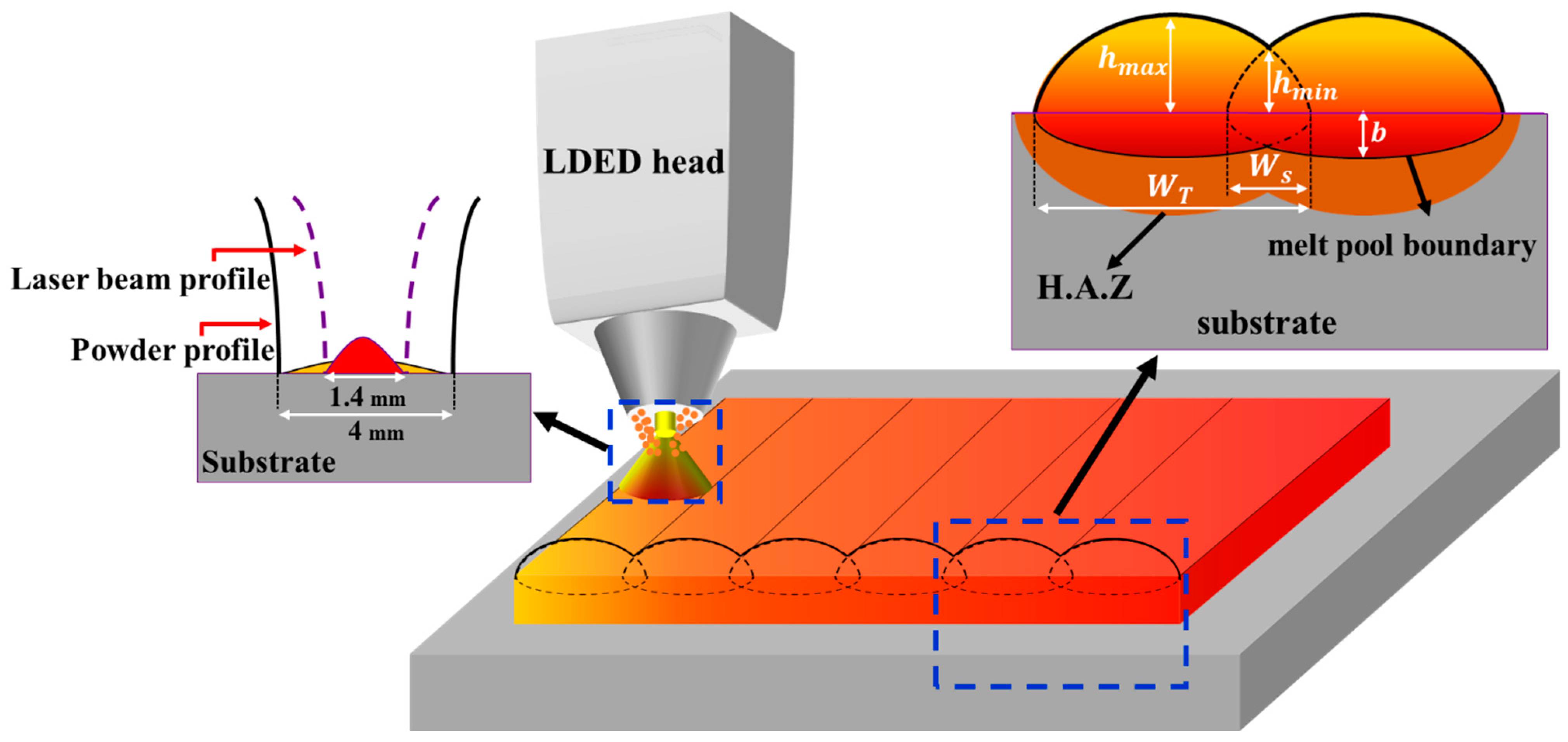
The CuCrZr powder was used as the feedstock material in this study and its characteristics were described in the authors’ previous study [26].

2.1. LDED Process

Single-layer multitrack with a nominal dimension of 10 × 10 mm and three sets of experiments were conducted for each condition, where a bidirectional method was employed to place them on the copper substrate. The deposition process was carried out using a powder-fed LDED system (IC106, DM3D Technology, Auburn Hills, MI, USA) with a robot (ABB IRB 140, Auburn Hills, MI, USA). The robot was equipped with a coaxial nozzle and a continuous wave disk laser (TruDisk 2000, TRUMPF, Ditzingen, Germany), which operated at 1030 nm and could deliver a maximum power of 2000 W. Figure 1 shows the LDED processing setup along with a magnified view of some deposited samples. Throughout the experiments, a consistent laser spot size of 1.4 mm was maintained. The primary focus of this investigation revolved around the main process parameters; the laser power (P, 900–1600 W), scanning speed (V, 4–8 mm/s), powder feed rate (F, 4–8 g/min), and the overlap ratio (OR), which is defined as the ratio of the overlapping distance of two tracks over the total distance from one end to the other.

2.2. Macro- and Micro-Scale Characterization

Metallographic characterization was performed to examine the geometrical characteristics and microstructure of the samples. Initially, three replicates per process condition were cross-sectioned and embedded in a conductive epoxy resin. Subsequently, the samples underwent grinding and polishing using SiC grinding papers with grit sizes ranging from 120 to 4000, followed by polishing with a 1 µm alumina slurry. Lastly, the polished samples were etched with a 50% HNO3 diluted in ethanol solution for 30 to 35 s, allowing their microstructure to be revealed.
The optical microscopy was performed using a Keyence VHX-7000 (500 Park Boulevard, Suite 200, Itasca, IL 60143, USA) digital microscope to examine the entire deposition from the top and observe the melt pool on the metallographically prepared samples. As shown in Figure 2, a single-layer multitrack consists of three discrete zones: overlapping deposited tracks, heat-affected zone (HAZ), and substrate. The measured geometrical characteristics of the deposition are the maximum height ( h m a x ), the minimum height ( h m i n ), the total width ( W T ), overlapping width ( W S ), and melt pool penetration depth (b). In addition, the surface roughness of the samples was measured from the top to bottom at multiple sections and S a number, which is the arithmetical mean height of the surface, was extracted and reported for each measurement.
In addition, the microstructure of the samples was analyzed using a Tescan VEGA3 scanning electron microscope (SEM, Brno, The Czech Republic). For further analysis, A Bruker QUANTAX electron backscatter diffraction (EBSD) apparatus was utilized at 20 kV voltage, employing a scanning step size of 4 μm. This setup was used to inspect the grain morphology and size. The data collected from EBSD analysis were then analyzed using ESPRIT2 software to obtain detailed information about the grain structure and orientation.

2.3. Porosity Measurements (XCT)

The as-built cuboids up to ~10 mm in height were examined for porosity distribution using ZEISS Xradia 520 Versa X-ray computed tomography (XCT) system. Overall, 1601 2D scanning projections at 140 kV with an exposure time of 1 s and a voxel size of 5 µm were conducted. Reconstruction of the images was performed using a beam hardening constant of 0.05, and the obtained scans were post-processed and analyzed in Dragonfly 3.1 software.

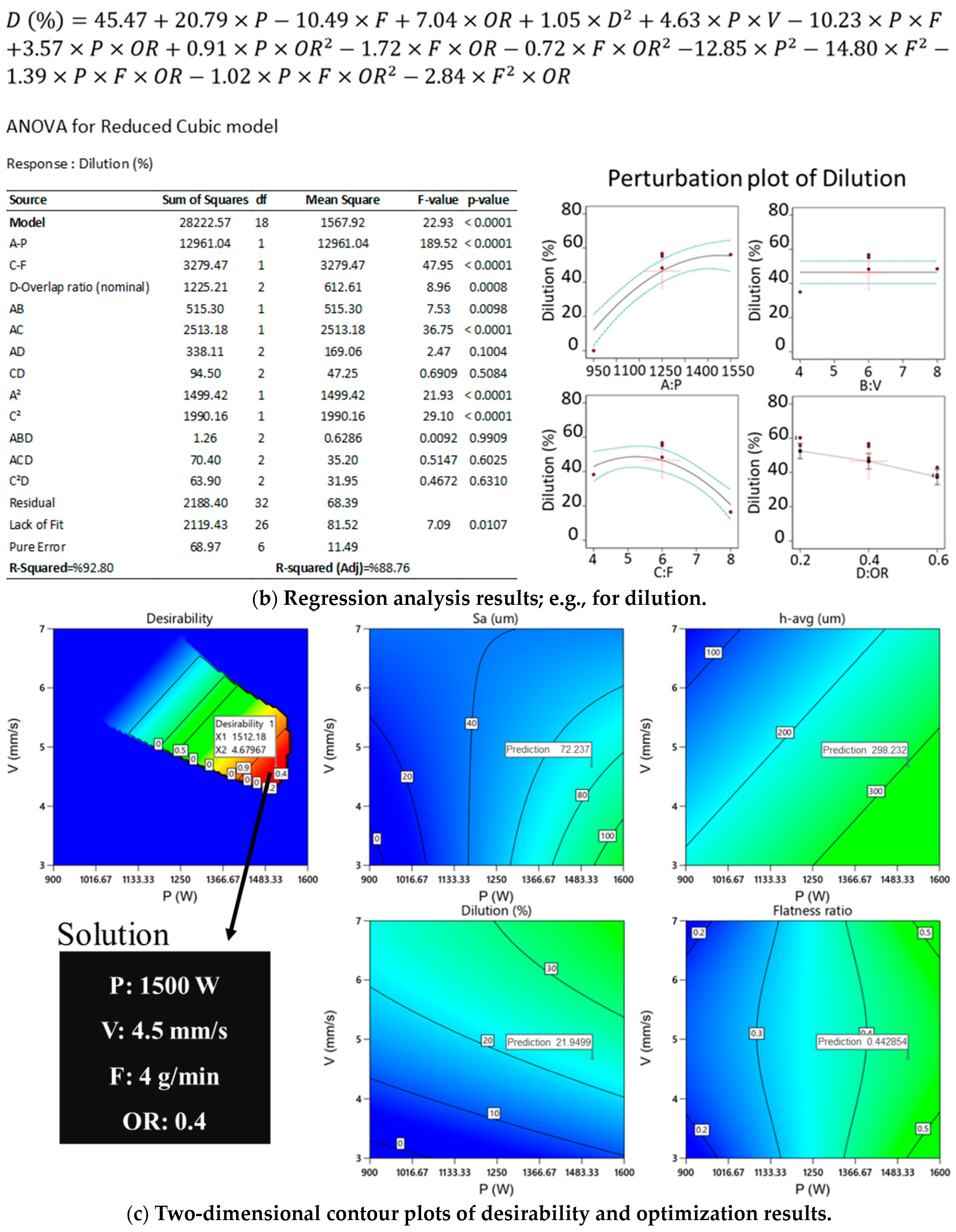
2.4. Statistical Analysis

In the realm of statistical data analysis, a three-step statistical approach utilized the response surface methodology (RSM). To define the range of process parameters in the experiments, the optimal processing window established in a preceding study involving CuCrZr single tracks [26] was adopted. Subsequently, by applying the central composite design (CCD) method, the design of experiments (DOE) was directed, followed by implementing a regression analysis on the responses (geometrical attributes). This aimed to establish a correlation between multitrack features and process parameters. The compliance function objectives comprised average height ( h a v g ), surface roughness ( S a ), dilution (D), and flatness ratio (S). All stages of data analysis, spanning from DOE to optimization, were executed using Design-Expert 13 software. For the DOE, a four-factor CCD matrix with an alpha value of 1 (face-centered) was employed, encompassing 51 runs with 3 replicates per condition. Table 1 details the input variables and output responses of the DOE matrix.

3. Results and Discussions

3.1. Process Parameter Optimization of Single-Layer Multitracks

Figure 3a discloses a general view of the geometrical measurement of a multitrack deposition. Following the collection of all response measurements, the RSM analysis was performed, and optimizing the process parameters then followed. The fitted model equation as well as the table of ANOVA and the perturbation plot are shown for the dilution response, as an example, in Figure 3b. The compliance function was set to maximize the average height ( h a v g ) and minimizing both the flatness ratio (S), and surface roughness (Sa), while keeping the dilution (D) in the range of 20–30%, as these are the mean values that are considered satisfactory for the LDED procedure [27,28,29,30]. The optimization solution, shown in Figure 3c, offered the set of process parameters for P, V, F, and OR to be 1500 W, 4.5 mm/s, 4 g/min, and 0.4, respectively, that altogether would result in the highest desirability criteria (1). To ascertain these specified process parameters as the optimal selection and to validate the optimization process, it was printed with a set of three replicates and the outcome is depicted in Figure 3d. For the anticipated responses, the average of measured values from experiments exhibited a favorable concurrence with both the lower and upper bounds of 95% confidence intervals.

3.2. Multi-Layer Build-Up and Trajectory Planning

In order to build up a multilayer cuboid geometry, the multitrack one-layer need to be deposited on top of each other repeatedly using the optimum set of process parameters. Yet, even if the single layer height is uniform, which it practically is not, the superimposition of single layers seldom leads to a high dimensional accuracy over multiple layers. More specifically, in robotic LDED systems, the movement of the robot arm during deposition can be categorized into three distinct phases: initial acceleration to attain the desired speed, consistent uniform motion, and eventual deceleration as the process concludes. In the acceleration and deceleration phases, employing a reduced scan speed contributes to an elevated heat input. As a result, this translates into an increased deposition rate and heightened accumulation of heat. Furthermore, insufficient deposition rates in proximity to edges primarily trigger deviations and the emergence of raised formations during the build-up process [31]. Therefore, proper build-up strategies and techniques must be considered for tool path trajectory planning to reach the near net shape of the desired geometry.
Figure 4 shows the schematics of the multiple techniques that were implemented in tool path trajectory planning along with their effect on the shape accuracy. As shown in Figure 4a, in this study, the zigzag deposition strategy with 90-degree rotation in the deposition direction between each layer is selected as the standard infill method. The unidirectional strategy (offset pattern) was not chosen due to the low deposition rate. Spiral inward/outward pattern is also not suitable for regular cuboid geometries because they cause varying scan-length and potentially higher heat accumulation near the center due to shorter cooling intervals between overlapping laser passes. In addition, as depicted in Figure 4b, the starting point was constantly rotated after each layer to balance out the varying deposition height in each layer. Figure 4c shows the profile contouring after the infill deposited layer and its effect that was considered to avoid the common dome-shaped issue. In fact, due to the lower deposition rate at the edges of the cuboid, the perimeter remained unfilled to some extent, which was tackled by adding one-line contouring with a proper amount of overlap with the previously deposited infill layer. Although the profile contouring maintained the squareness of the cuboid built-up, it resulted in arisen corners due to the higher deposition at those regions. Thus, as shown in Figure 4d, for the corners of the contour’s path, an arc with a radius of 0.7 mm, which is half of the melt pool width, was considered. This resulted in avoiding sharp corners, which creates a delay in changing direction and therefore higher deposition at the corners. All the aforementioned techniques were employed to reach the cuboid build-up with an acceptable shape accuracy, as shown in Figure 4d.

3.3. Defects and XCT Results

Besides the process parameter optimization and correct toolpath trajectory planning, there are some other issues that can appear through multilayer fabrication and need to be tackled. As such, surface dimples have been seen on the top layer of some specimens with specific process parameters. In that regard, investigation has been conducted on the effect of process parameters on the surface dimples effect and results have been illustrated in Figure 5. Using the set of process parameters that was optimized for multitrack single-layer and the correct tool path trajectory, surface dimples appeared as shown in Figure 5a from the top view and in the cross-section. Yet, increasing the laser power from 1500 to 2000 W resolved this issue. Moreover, in another case shown in Figure 5b, increasing the scanning speed from 4 to 8 mm/s also resulted in disappearance of these defects. After giving a precise look at the cross-section of the samples and putting all the parameters together, it was concluded that the source of the surface dimples is, in fact, the lack of fusion, which is one of the most common issues in LDED.
LOF porosity can be identified by its large and irregularly shaped pores and often contain unmelted powder particles similar to what has been observed from the cross-section of defective samples in Figure 5. These defects are normally attributed to incorrect processing parameters and/or conditions such as oxidation during the deposition process, which is the case in this study as the process takes place in an ambient atmosphere and decreases the efficiency of input energy such that not all powder particles are completely melted or the previously deposited layer is not sufficiently remelted to fuse with the new layer. For the CuCrZr multilayer, processing parameters are investigated and it can be readily observed that LOF porosity occupies the low laser power, and low scanning speed that leads to high F/V, which indicates the amount of powder that is fed to the meltpool and the deposition thickness. It is worth mentioning that although the lower scanning speed increases the energy density to some extent, its effect on the F/V value is stronger based on the observations in this study. This behavior agrees well with the general hypothesis that points to low power input per the amount of material or alternatively low energy density as the primary source of LOF porosity.
In that regard, Tang et al. [9] developed Equation (1) that predicts the LOF defect, which is schematically shown in Figure 6a, based on the geometrical parameters and characteristics of the melt pool:
h b 2 + H W 2 1
in which h is the deposition height, b is the melt pool penetration depth, H is the hatching distance, and W is the melt pool width. Based on this equation, measurements were conducted on some defective and fine samples, and results are plotted in Figure 6b where four samples were selected for porosity analysis using the XCT scan technique. As shown in the plot, both samples 1 and 2 are inside the LOF quadrant and do not have any sign of LOF defects, while the samples 3 and 4 are located outside of the criterion and have a noticeable amount of LOFs. These results show that the CuCrZr buildup follows the LOF geometric criterion very well. As attained in the optimization procedure, the H/W (OR) value was defined to be 0.4, which consequently leaves the melt pool penetration depth and the deposition height as the only crucial parameters. Where the former is mainly controlled by the laser power and the latter is defined by the F/V value. Therefore, maintaining a constant value of energy density, which is the ratio of P to F/V, can avoid LOF in CuCrZr build-up.

Vaporization

The nature of a high-intensity laser beam with high power densities (> 10 5 W/mm2) and short interaction times (micro- to milliseconds) leads to vaporization and ejection of molten material during the deposition process, seen in Figure 7a. This phenomenon is not desirable in LDED and more preferable for laser drilling/cutting [7]. This vaporization results in a loss of alloying elements and keyhole formation, particularly in multilayer build-up that adversely affects the mechanical properties and microstructure. Here, in LDED of CuCrZr, the vaporization took place due to high laser power (from 1800 to 2000 W) per low F/V values (from 0.003 to 0.005 g/mm) that led to too much energy density and evaporation of material from the substrate.
Balling, which is the formation of the small ball-shape discontinuous deposition of melted powders on top of the substrate or previous layer [11,12], was observed in the single-layer multitrack samples. In fact, whenever the laser power is not sufficient to melt both the substrate and powders together, a stable melt pool cannot be formed and only partially melted powders that have relatively high solid–liquid interfacial free energy γ S L join together and poorly connect to the substrate instead of properly wetting it as seen in Figure 7b. The effects of surface tension also contribute to the formation of balling defects in LDED [32]. Balling occurs when the molten powder from the laser fails to wet the substrate due to oxide contamination on the melt’s surface. The wetting behavior of the liquid metal on oxide films is influenced by interfacial energies at solid–vapor, solid–liquid, and liquid–vapor interfaces. The spreading coefficient quantifies liquid behavior on a solid surface, which is defined as [33]:
S = γ S V γ S L γ L V
where γ S V is solid–vapor interfacial free energy, γ S L is solid–liquid interfacial free energy, and γ L V is the liquid–vapor interfacial free energy. A positive value of S would result in wetting the solid interface by the liquid, whereas the negative values lead to balling phenomenon. For metal oxides, the solid–vapor surface free energy is lower than the liquid–vapor surface free energy, resulting in a negative spreading coefficient [34]. As a consequence, the liquid metal tends to minimize the surface area by forming ball-like structures instead of spreading and wetting the oxide films on the melt’s surface. Therefore, by increasing the laser power, enough energy to break the surface oxides is provided as well as a deeper penetration of the laser beam into the material that results in a larger molten pool and improving wetting between the solid and liquid phases [35].
The parameters that cause balling in single-layer can often bring about defects when they are used for multilayer buildup. These defects include large pores, inclusions, and poor surface roughness [12].

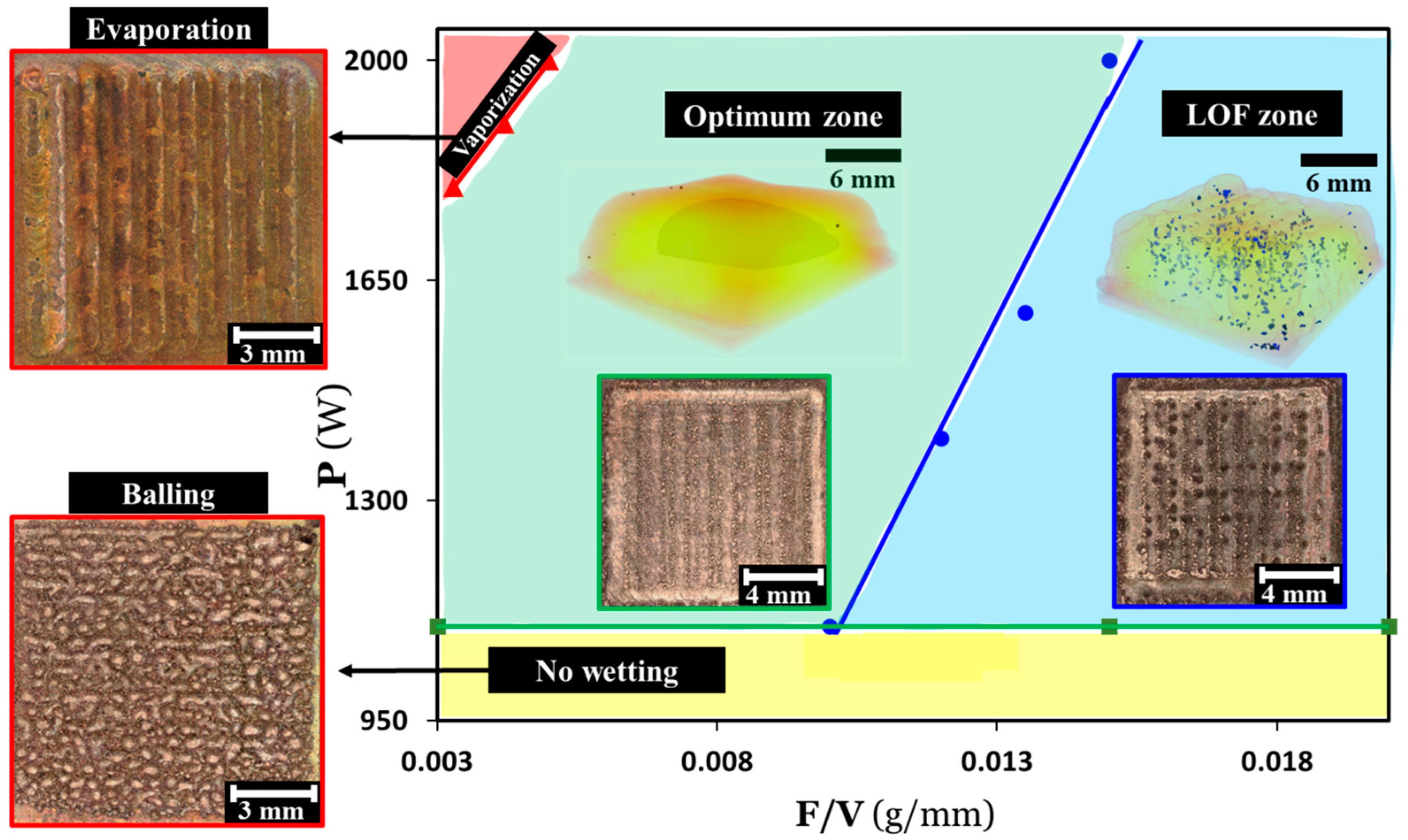
3.4. General Processing Map

Taking into account all the data together, the general processability map of CuCrZr via LDED technique is drawn based on the key process parameters of laser power (P) per F/V values. As seen in the yellow region, the green straight line shows the minimum laser power of 1100 W that is needed for the fed powders to properly melt and wet the previous layer/substrate and form a stable melt pool and avoid the balling defect. Above the green line in the blue region, the blue line is fit to the data that have a few LOF defects and draws the boundary between the blue and green regions, which define the LOF-rich and fine deposition regions, respectively. In the green region, only a few spherical gas porosities have been seen in the samples, which is common and acceptable in LDED as there are always gas pores that are entrapped in the powder particles and/or oxidation during the process. Separated by the red line from the green region, the red region stands for too-high values of power per relatively low values of F/V that results in vaporization of the powder and substrate material, which is not a desirable phenomenon in LDED. Therefore, as shown in Figure 8, for optimum deposition of CuCrZr alloy, both the P and F/V values must be kept in the green deposition region. All the aforementioned instabilities and defects in LDED processing of CuCrZr alloy are directly correlated to both P and F/V as key process parameters, and having a processing map that identifies defects based on these parameters is highly valuable.

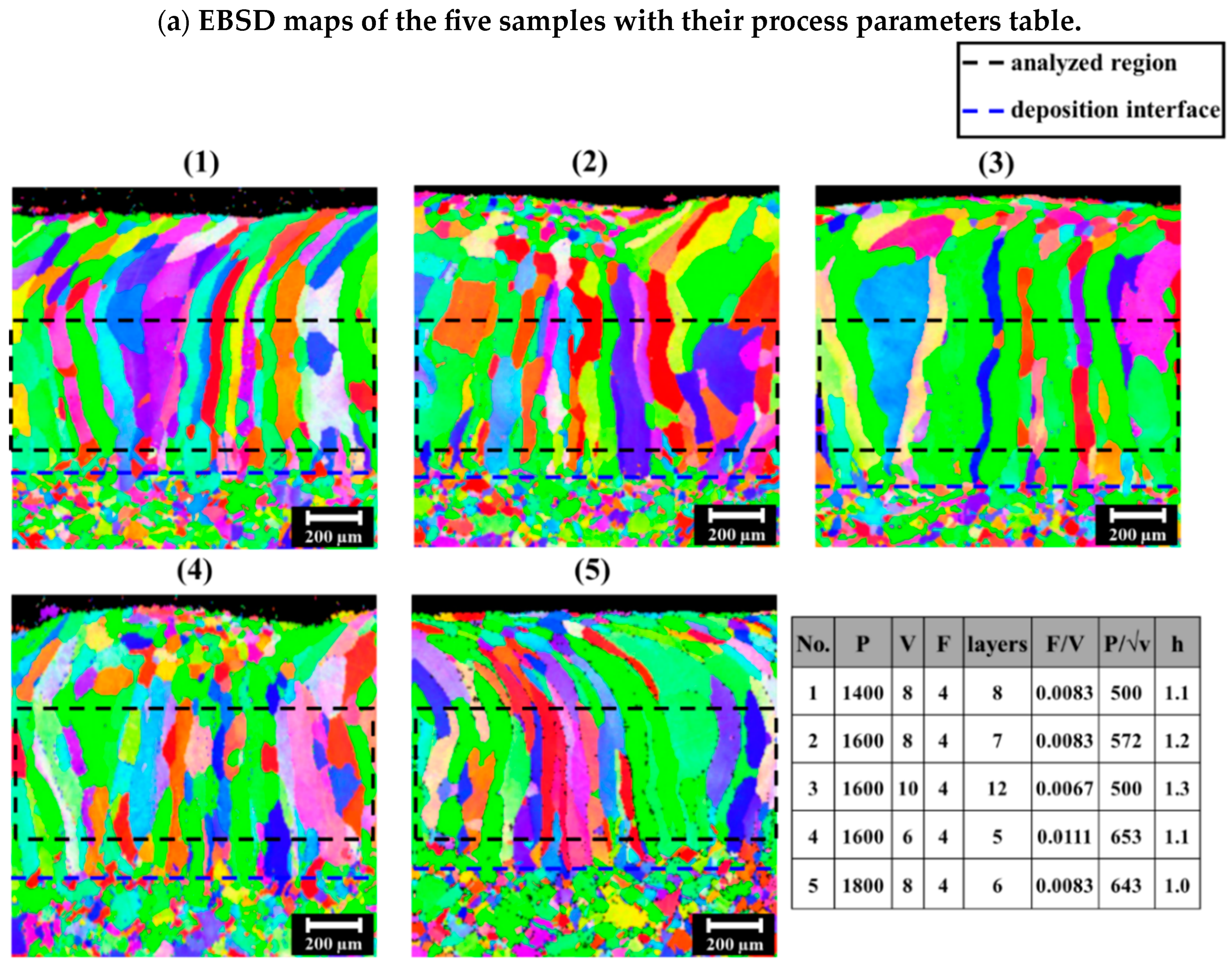
3.5. Microstructural Results

The microstructure of the LDED deposited samples is directly influenced by the main process parameters. As such laser power, scanning speed, powder feed rate, and number of layers are the parameters that have been frequently identified as the key parameters influencing the microstructure during multilayer deposition [36,37]. In a single melt pool, solidification is directly influenced by the laser power, scanning speed, and feed rate that altogether control the geometry, thermal gradient, solidification speed, and number of nucleation sites. On the other hand, during the multilayer build-up process with LDED, the multiple deposition of single layers on top of each other leads to re-melting and inducing thermal cycles in the previously deposited material that leads to recrystallization and grain growth in the microstructure [37].
To identify the effect of process parameters on the microstructure, five cuboid samples are printed with almost the same height but different process parameters that are still in the green region of the processability map (Figure 8) and results from EBSD analysis are shown in Figure 9. The grain structure of all the samples with their process parameters are illustrated in Figure 9a in which highly columnar grains are grown from the fusion zone interface with the substrate towards the curved top surface of the deposit. Near the boundary of the pool, where the pool is nearly orthogonal to the observed cross-section, the grain growth direction is approximately in plane with the transverse section, as a result of epitaxial grain growth mechanism and high values of G vs. R [38,39]. Yet in the very top region and close to the surface, a fine equiaxed grain structure can be seen due to the relatively low values of G vs. R and more nucleation sites [38,40]. A certain area of the deposition region in the samples is selected for further analysis. The average grain size, average number of grains, and columnarity of the grain structure are illustrated in Figure 9b. Based on the average grain size results, sample 3′s grain structure is significantly coarser than sample 4, while its average number of grains is much smaller.
It is possible that the lower value of F/V, which identifies the amount of powder that is fed to the melt pool distance, leads to a reduced number of nucleation sites [39,41], which contributes to the number of grains and therefore their size. Additionally, a higher number of layers in sample 3 resulted in more cycles of reheating and cooling of the previously deposited material, and this in turn affects the temporal evolution of the grains and their sizes. The proposed mechanisms are further supported by the observation of a higher columnarity of the grain structure in sample 3. This suggests that the factors influencing the growth of the grains in this sample are consistent with the proposed mechanisms, and highlights the importance of considering multiple factors in understanding the evolution of grain structure. Therefore, different grain structures, which influence the mechanical properties [42], can be achieved for the same deposition height while still being in the optimum processing window.

4. Conclusions

In this work, multilayer buildup of CuCrZr alloy, which is a challenging material due to high heat conductivity and low laser absorption, was exercised via the LDED-PF process, and multivariate correlation between sample properties and process parameters was investigated. The present study focused on optimizing the key process parameters, printing strategy, and developing the optimum processing window that altogether results in a defect-free near-net shape multilayer cuboid geometry. For this purpose, the impact of different process parameter combinations, P and F/V, on different types of defects such as balling, evaporation, and LOF porosity was studied and a general processability map was drawn. Utilizing the combination of different process parameters from the optimum processing window, a set of samples with almost the same deposition height was built. This allowed us to evaluate the effect of process parameters on the microstructure. The results of the study can be summarized as follows:
  • To properly wet the substrate and form a stable melt pool, the minimum laser power of 1100 W is needed, otherwise the balling defect happens as a result of negative values of spreading factors, S.
  • The optimum set of parameters for single-layer multitrack is a laser of 1500 W, powder feed rate of 4 g/min, scanning speed of 4.5 mm/s, and overlap ratio of 0.4. The observed responses closely align with the values predicted by the model, demonstrating approximately 95% confidence intervals for both lower and upper bounds.
  • Tool path trajectory planning has been conducted to reach the proper build-up strategy that leads to acceptable shape accuracy. For the infill of the geometry, the zigzag strategy with 90° rotation of deposition direction in which the start point also rotates between layers is considered. Further, to compensate for the unfilled perimeter, profile contouring around the perimeter after each infill deposition was considered with a radial pathway at the corners to avoid the bumps that happen as a result of acceleration and deceleration of the robotic arm.
  • In order to avoid the LOF defect, the melt pools need to properly overlap each other, both horizontally and vertically. In that regard, the LOF quadrant criterion is employed based on h/b and H/W that define the amount of vertical and horizontal overlap, respectively. Based on the XCT scan results, it was shown that as far as the criterion of h b 2 + H W 2 < 1 is met, no LOF would happen in the multilayer cuboid samples. Therefore, per amount of fed powder to the melt pool (F/V) minimum energy (P) is needed to reach sufficient values of melt pool depth (b) and width (W) to avoid LOF.
  • While insufficient values of P per F/V results in LOF defect, too high values are also deleterious and lead to the vaporization of fed powders and substrate material.
  • The general processability map was drawn by putting all the data together and based on the P against F/V parameters. The optimum processing window is defined by green color in which only a small amount of gas porosity defects can exist, which are inevitable and common in the LDED process.
  • The grain structure of the deposition mainly consists of big columnar grains that nucleated from the fusion zone and grew up to the very top layer through the epitaxial grain growth mechanism. Yet on the very top layer and close to the surface, the fine and equiaxed grain structure has been observed due to the relatively lower values of G vs. R and more nucleation sites. Depositing the new layer provides reheating and cooling for the formerly deposited layer, which leads to grain growth and increases the grain size.
  • Utilizing the combinations of process parameters from the optimum processing window for the same deposition height, it was shown that the number of layers as well as the F/V value are influencing the grain size. While the former affects the amount of reheating in the previously deposited material, the latter provides the number of nucleation sites and therefore the number of grains. The higher the number of layers and the lower F/V, the bigger the grain size.

Author Contributions

A.Z.: Conceptualization, Methodology, Software, Validation, Formal analysis, Investigation, Writing—original draft, Writing—review & editing, Visualization; R.E.: Methodology, Investigation, Writing—review & editing; M.A.: Investigation, Writing—review & editing; M.K.K.: Investigation, Writing—review & editing; H.J.: Conceptualization, Supervision; E.T.: Conceptualization, Writing—review & editing, Supervision, Project administration, Funding acquisition. All authors have read and agreed to the published version of the manuscript.

Funding

This study was supported by funding from the Natural Sciences and Engineering Research Council of Canada (NSERC), the Federal Economic Development Agency for Southern Ontario (FedDev Ontario).

Data Availability Statement

All data generated or analyzed during this study are available within the article.

Conflicts of Interest

The authors declare no conflict of interest.

Abbreviations

LDEDLaser-directed energy deposition
SEMscanning electron microscope
EBSDelectron backscatter diffraction
EDSenergy dispersive X-ray spectroscope
HAZheat affected zone
AMadditive manufacturing
DOEdesign of experiment
CCDcentral composite design
RSMresponse surface methodology

References

  1. Toyserkani, E.; Sarker, D.; Ibhadode, O.O.; Liravi, F.; Russo, P.; Taherkhani, K. Metal Additive Manufacturing; Wiley: Hoboken, NJ, USA, 2021. [Google Scholar]
  2. Frazier, W.E. Metal Additive Manufacturing: A Review. J. Mater. Eng. Perform. 2014, 23, 1917–1928. [Google Scholar] [CrossRef]
  3. Fayazfar, H.; Salarian, M.; Rogalsky, A.; Sarker, D.; Russo, P.; Paserin, V.; Toyserkani, E. A critical review of powder-based additive manufacturing of ferrous alloys: Process parameters, microstructure and mechanical properties. Mater. Des. 2018, 144, 98–128. [Google Scholar] [CrossRef]
  4. Guo, C.; He, S.; Yue, H.; Li, Q.; Hao, G. Prediction modelling and process optimization for forming multi-layer cladding structures with laser directed energy deposition. Opt. Laser Technol. 2021, 134, 106607. [Google Scholar] [CrossRef]
  5. Chen, C.; Lian, G.; Jiang, J.; Wang, Q. Simplification and experimental investigation of geometrical surface smoothness model for multi-track laser cladding processes. J. Manuf. Process. 2018, 36, 621–628. [Google Scholar] [CrossRef]
  6. Ng, G.K.L.; Jarfors, A.E.W.; Bi, G.; Zheng, H.Y. Porosity formation and gas bubble retention in laser metal deposition. Appl. Phys. A 2009, 97, 641–649. [Google Scholar] [CrossRef]
  7. Steen, W.M.; Mazumder, J. Laser Material Processing; Springer Science & Business Media: Berlin, Germany, 2010. [Google Scholar]
  8. Cunningham, R.W. Defect Formation Mechanisms in Powder-Bed Metal Additive Manufacturing. Doctoral Dissertation, Carnegie Mellon University, Pittsburgh, PA, USA, 2018. [Google Scholar]
  9. Tang, M.; Pistorius, P.C.; Beuth, J.L. Prediction of lack-of-fusion porosity for powder bed fusion. Addit. Manuf. 2017, 14, 39–48. [Google Scholar] [CrossRef]
  10. Cunningham, R.; Zhao, C.; Parab, N.; Kantzos, C.; Pauza, J.; Fezzaa, K.; Sun, T.; Rollett, A.D. Keyhole threshold and morphology in laser melting revealed by ultrahigh-speed x-ray imaging. Science 2019, 363, 849–852. [Google Scholar] [CrossRef]
  11. Yadroitsev, I.; Gusarov, A.; Yadroitsava, I.; Smurov, I. Single track formation in selective laser melting of metal powders. J. Mater. Process. Technol. 2010, 210, 1624–1631. [Google Scholar] [CrossRef]
  12. Kiani, P.; Dupuy, A.D.; Ma, K.; Schoenung, J.M. Directed energy deposition of AlSi10Mg: Single track nonscalability and bulk properties. Mater. Des. 2020, 194, 108847. [Google Scholar] [CrossRef]
  13. DebRoy, T.; Wei, H.L.; Zuback, J.S.; Mukherjee, T.; Elmer, J.W.; Milewski, J.O.; Beese, A.M.; Wilson-Heid, A.; De, A.; Zhang, W. Additive manufacturing of metallic components–Process, structure and properties. Prog. Mater. Sci. 2018, 92, 112–224. [Google Scholar] [CrossRef]
  14. Nankali, M.; Akbari, J.; Moradi, M.; Beiranvand, Z.M. Effect of laser additive manufacturing parameters on hardness and geometry of Inconel 625 parts manufactured by direct laser metal deposition. Optik 2022, 249, 168193. [Google Scholar] [CrossRef]
  15. Mortello, M.; Casalino, G. Transfer mode effects on Ti6Al4V wall building in wire laser additive manufacturing. Manuf. Lett. 2021, 28, 17–20. [Google Scholar] [CrossRef]
  16. Bonesso, M.; Rebesan, P.; Gennari, C.; Mancin, S.; Dima, R.; Pepato, A.; Calliari, I. Effect of particle size distribution on laser powder bed fusion manufacturability of copper. Berg Huettenmaenn. Mon. 2021, 166, 256–262. [Google Scholar] [CrossRef]
  17. Agostinetti, P.; Benedetti, E.; Bonifetto, R.; Bonesso, M.; Cavenago, M.; Bello, S.D.; Palma, M.D.; D’Ambrosio, D.; Dima, R.; Favero, G.; et al. Improved Conceptual Design of the Beamline for the DTT Neutral Beam Injector. IEEE Trans. Plasma Sci. 2022, 50, 4027–4032. [Google Scholar] [CrossRef]
  18. Popovich, A.; Sufiiarov, V.; Polozov, I.; Borisov, E.; Masaylo, D.; Orlov, A. Microstructure and mechanical properties of additive manufactured copper alloy. Mater. Lett. 2016, 179, 38–41. [Google Scholar] [CrossRef]
  19. Guan, P.; Chen, X.; Liu, P.; Sun, F.; Zhu, C.; Zhou, H.; Fu, S.; Wu, Z.; Zhu, Y. Effect of selective laser melting process parameters and aging heat treatment on properties of CuCrZr alloy. Mater. Res. Exp. 2019, 6, 1165–1166. [Google Scholar] [CrossRef]
  20. Lassègue, P.; Salvan, C.; De Vito, E.; Soulas, R.; Herbin, M.; Hemberg, A.; Godfroid, T.; Baffie, T.; Roux, G. Laser powder bed fusion (L-PBF) of Cu and CuCrZr parts: Influence of an absorptive physical vapor deposition (PVD) coating on the printing process. Addit. Manuf. 2021, 39, 101888. [Google Scholar] [CrossRef]
  21. Bergström, D.; Powell, J.; Kaplan, A.F.H. Absorptance of nonferrous alloys to Nd:YLF and Nd:YAG laser light at room temperature. Appl. Opt. 2007, 46, 1290–1301. [Google Scholar] [CrossRef]
  22. Ordás, N.; Portolés, L.; Azpeleta, M.; Gómez, A.; Blasco, J.R.; Martinez, M.; Ureña, J.; Iturriza, I. Development of CuCrZr via Electron Beam Powder Bed Fusion (EB-PBF). J. Nucl. Mater. 2021, 548, 152841. [Google Scholar] [CrossRef]
  23. Gradl, P.R.; Protz, C.S. Technology advancements for channel wall nozzle manufacturing in liquid rocket engines. Acta Astronaut. 2020, 174, 148–158. [Google Scholar] [CrossRef]
  24. Gradl, P.R.; Greene, S.E.; Protz, C.; Bullard, B.; Buzzell, J.; Garcia, C.; Wood, J.; Osborne, R.; Hulka, J.; Cooper, K.G. Additive Manufacturing of Liquid Rocket Engine Combustion Devices: A Summary of Process Developments and Hot-Fire Testing Results. In Proceedings of the 2018 Joint Propulsion Conference, Cincinnati, OH, USA, 9–11 July 2018. [Google Scholar]
  25. Horn, T.J.; Gamzina, D. Additive Manufacturing of Copper and Copper Alloys; ASM International: Novelty, OH, USA, 2020; pp. 388–418. [Google Scholar]
  26. Zardoshtian, A.; Ansari, M.; Esmaeilzadeh, R.; Keshavarzkermani, A.; Jahed, H.; Toyserkani, E. Laser-directed energy deposition of CuCrZr alloy: From statistical process parameter optimization to microstructural analysis. Int. J. Adv. Manuf. Technol. 2023, 126, 4407–4418. [Google Scholar] [CrossRef]
  27. Sun, Y.; Hao, M. Statistical analysis and optimization of process parameters in Ti6Al4V laser cladding using Nd:YAG laser. Opt. Lasers Eng. 2012, 50, 985–995. [Google Scholar] [CrossRef]
  28. Ansari, M.; Mohamadizadeh, A.; Huang, Y.; Paserin, V.; Toyserkani, E. Laser directed energy deposition of water-atomized iron powder: Process optimization and microstructure of single-tracks. Opt. Laser Technol. 2019, 112, 485–493. [Google Scholar] [CrossRef]
  29. Ansari, M.; Razavi, R.S.; Barekat, M. An empirical-statistical model for coaxial laser cladding of NiCrAlY powder on Inconel 738 superalloy. Opt. Laser Technol. 2016, 86, 136–144. [Google Scholar] [CrossRef]
  30. Dass, A.; Moridi, A. State of the Art in Directed Energy Deposition: From Additive Manufacturing to Materials Design. Coatings 2019, 9, 418. [Google Scholar] [CrossRef]
  31. Wang, M.; Kashaev, N. On the optimal process window for powder-based laser-directed energy deposition of AA7050 under different robot programs and scanning strategies. J. Manuf. Process. 2023, 90, 286–299. [Google Scholar] [CrossRef]
  32. Gu, D.D.; Shen, Y.F. Influence of phosphorus element on direct laser sintering of multicomponent Cu-based metal powder. Metall. Mater. Trans. B 2006, 37, 967–977. [Google Scholar] [CrossRef]
  33. Das, S. Physical aspects of process control in selective laser sintering of metals. Adv. Eng. Mater. 2003, 5, 701–711. [Google Scholar] [CrossRef]
  34. Bunnell, D.E. Fundamentals of Selective Laser Sintering of Metals; The University of Texas at Austin: Austin, TX, USA, 1995. [Google Scholar]
  35. Grange, D.; Queva, A.; Guillemot, G.; Bellet, M.; Bartout, J.D.; Colin, C. Effect of processing parameters during the laser beam melting of Inconel 738: Comparison between simulated and experimental melt pool shape. J. Mater. Process. Technol. 2021, 289, 116897. [Google Scholar] [CrossRef]
  36. Wei, H.L.; Mukherjee, T.; Debroy, T. Grain growth modeling for additive manufacturing of nickel based superalloys. In Proceedings of the 6th International Conference on Recrystallization and Grain Growth (ReX&GG 2016), Pittsburgh, PA, USA, 17–21 July 2016; Springer: Berlin/Heidelberg, Germany, 2016; pp. 265–269. [Google Scholar]
  37. Wei, H.L.; Knapp, G.L.; Mukherjee, T.; DebRoy, T. Three-dimensional grain growth during multi-layer printing of a nickel-based alloy Inconel 718. Addit. Manuf. 2019, 25, 448–459. [Google Scholar] [CrossRef]
  38. Ansari, M.; Martinez-Marchese, A.; Khamooshi, M.; Keshavarzkermani, A.; Esmaeilizadeh, R.; Toyserkani, E. Analytical modeling of multi-track powder-fed laser directed energy deposition: On the relationships among process, deposition dimensions, and solidification microstructure in additively manufactured near-β titanium alloy. J. Mater. Process. Technol. 2022, 306, 117643. [Google Scholar] [CrossRef]
  39. Keshavarzkermani, A.; Marzbanrad, E.; Esmaeilizadeh, R.; Mahmoodkhani, Y.; Ali, U.; Enrique, P.D.; Zhou, N.Y.; Bonakdar, A.; Toyserkani, E. An investigation into the effect of process parameters on melt pool geometry, cell spacing, and grain refinement during laser powder bed fusion. Opt. Laser Technol. 2019, 116, 83–91. [Google Scholar] [CrossRef]
  40. Keshavarzkermani, A.; Sadowski, M.; Ladani, L. Direct metal laser melting of Inconel 718: Process impact on grain formation and orientation. J. Alloys Compd. 2018, 736, 297–305. [Google Scholar] [CrossRef]
  41. Sreekanth, S.; Ghassemali, E.; Hurtig, K.; Joshi, S.; Andersson, J. Effect of Direct Energy Deposition Process Parameters on Single-Track Deposits of Alloy 718. Metals 2020, 10, 96. [Google Scholar] [CrossRef]
  42. Keshavarzkermani, A.; Esmaeilizadeh, R.; Ali, U.; Enrique, P.D.; Mahmoodkhani, Y.; Zhou, N.Y.; Bonakdar, A.; Toyserkani, E. Controlling mechanical properties of additively manufactured hastelloy X by altering solidification pattern during laser powder-bed fusion. Mater. Sci. Eng. A 2019, 762, 138081. [Google Scholar] [CrossRef]
Figure 1. Schematic of the LDED setup with a magnified view of some deposited samples.
Jmmp 07 00151 g001
Figure 2. Schema of LDED single-layer multitrack deposition and its geometrical characteristics.
Jmmp 07 00151 g002
Figure 3. (a) Responses and geometrical measurements of a multitrack one-layer, (b) regression analysis results for dilution as an example, (c) optimization solution and desirability plot, and (d) validation of the optimization results.
Jmmp 07 00151 g003aJmmp 07 00151 g003bJmmp 07 00151 g003c
Figure 4. Schematic of the strategies that have been considered for tool path trajectory planning; (a) infill zigzag trajectory with 90° rotation of scanning direction between layers, (b) the effect of start point rotation for the laser on geometrical accuracy, (c) the effect of addition of profile contouring around the perimeter, and (d) the effect of addition of radial pathway at the corners of the contours.
Jmmp 07 00151 g004
Figure 5. (a) Effect of laser power and (b) scanning speed on surface dimples.
Jmmp 07 00151 g005
Figure 6. (a) Schematic of lack of fusion defect, (b) lack of fusion map of CuCrZr multilayer samples.
Jmmp 07 00151 g006
Figure 7. (a) Vaporization and (b) poor wetting as results of excessive and insufficient power per F/V, respectively.
Jmmp 07 00151 g007
Figure 8. General LDED processability map of CuCrZr alloy.
Jmmp 07 00151 g008
Figure 9. Microstructural analysis of multilayer CuCrZr (a) EBSD maps and process parameter table of the five samples with almost the same deposition height, (b) grain structure analysis results.
Jmmp 07 00151 g009aJmmp 07 00151 g009b
Table 1. The input variables and output responses of the DOE.
Track NO.Process Parameters
(Input Variables)
Geometrical Measurements
(Output Responses)
P (W)V (mm/s)F (g/min)OR h a v g (µm)Sa (µm)D (%)S
11250660.291.1517.3755.750.57
2950440.2604101
31550660.4163.4732.2556.150.61
4950840.6193.2333.1300.43
51250660.6232.3947.1338.390.52
61250860.271.1315.8357.700.50
7950660.4205.5955.700.26
8950840.256.9331.5101
91250660.4122.9027.148.300.63
10950480.4282.3588.1200.51
111550480.6615.88243.174.340.88
121550440.488.9222.6454.170.64
13950660.6313.476000.44
141550880.6308.2065.8322.100.52
151250860.4102.9220.2148.530.57
161250660.4117.4424.7355.220.66
17950480.2204.3262.1500.59
18950440.6184.3734.7100.51
191250460.4162.4429.8134.980.56
201250460.6247.3442.5726.100.53
211550480.4387.7291.316.730.59
221550880.4217.2946.5528.700.62
231550660.6231.8546.8847.440.59
241250680.4188.8539.9116.480.63
251250640.4122.0119.7938.270.52
26950880.2314.7772.2500.35
27950480.6613.93167.200.60
281250460.2132.3434.1939.770.69
291250660.295.9022.560.160.66
301250660.4110.3530.1156.750.81
311550480.2268.9981.829.420.69
321250860.6128.7629.4242.980.54
331250680.6393.95124.568.640.74
34950880.61213.51495.2100.80
35950840.468.6020.8700.70
361550840.470.1815.7771.270.67
371250660.295.481860.270.61
381250660.6192.0645.4542.990.79
39950880.4408.05106.9200.48
40950440.496.7326.4400.59
411250680.2141.3230.9420.870.62
42950660.2137.4635.8700.45
431550660.297.6021.7968.200.73
441550440.271.4919.1359.520.71
451550840.6154.7225.152.950.55
461250640.276.8620.7949.600.70
471550840.259.0211.9674.680.56
481550440.6186.3443.3936.060.65
491250640.6213.1050.926.190.60
501550880.2187.8842.5431.760.63
511250660.6235.5452.4938.0780.64
Disclaimer/Publisher’s Note: The statements, opinions and data contained in all publications are solely those of the individual author(s) and contributor(s) and not of MDPI and/or the editor(s). MDPI and/or the editor(s) disclaim responsibility for any injury to people or property resulting from any ideas, methods, instructions or products referred to in the content.

