Abstract
Additive manufacturing of metals is limited by a fundamental tradeoff between deposition rates and manufacturability of fine-scale features. To overcome this problem, a laser-ablated bound metal deposition (laBMD) process is demonstrated in which 3D-printed green-state bound metal deposition (BMD) parts are post-processed via laser ablation prior to conventional BMD debinding and sintering. The laBMD process is experimentally characterized via a full-factorial design of experiments to determine the effect of five factors—number of laser passes (one pass, three passes), laser power (25%, 75%), scanning speed (50%, 100%), direction of laser travel (perpendicular, parallel), and laser resolution (600 dpi, 1200 dpi)—on as-sintered ablated depth, surface roughness, width, and angle between ablated and non-ablated regions. The as-sintered ablation depth/pass ranged from 3 to 122 µm/pass, the ablated surface roughness ranged from 3 to 79 µm, the angle between ablated and non-ablated regions ranged from 1° to 68°, and ablated bottom widths ranged from 729 to 1254 µm. This study provides novel insights into as-manufactured ablated geometries and surface finishes produced via laser ablation of polymer–metallic composites. The ability to inexpensively and accurately manufacture fine-scale features with tailorable geometric tolerances and surface finishes is important to a variety of applications, such as manufacturing molds for microfluidic devices.
1. Introduction
Additive manufacturing (AM) is a process to create 3D parts, typically in a layer-by-layer fashion. Of the seven AM processes defined within ASTM 52900 [1], five AM processes—binder jetting [2], directed energy deposition [3,4], material extrusion [5], powder bed fusion [4,6], and sheet lamination [7]—have been utilized for AM of metals (AMM). Beyond processes identified within ASTM 52900, friction stir welding [8], cold spraying [9], direct metal writing [10], and diode-based processes [11] have also been utilized for AMM.
Compared to subtractive manufacturing (SM) and formative manufacturing (FM), AMM has multiple advantages. For example, AMM can reduce lead times, enable mass customization, promote cost reductions via virtual inventories, and produce more complex geometries. These advantages have led to enhanced designs, including the F-15 pylon rib and the GE LEAP engine fuel nozzle [12]. Additionally, AMM opens entirely new design possibilities, including conformal cooling [13], lightweight structures [14], and mass customization [15].
Despite AMM’s advantages, challenges remain. For example, AMM is limited by inferior mechanical properties [16,17], high costs, slow deposition rates [18], poor resolution, and poor surface finish [19,20]. Importantly, some of the challenges represent tradeoffs in which improving one aspect is detrimental to another. For example, increasing the deposition rate often results in poorer geometric resolution and a poorer surface finish. These tradeoffs motivate a research question, i.e., can resolution be improved without negatively affecting deposition rates?
1.1. Bound Metal Deposition (BMD)
Bound metal deposition (BMD) is a plunger-based material extrusion process employed on Desktop Metal (DM) Studio+ systems and consists of three primary manufacturing steps: printing, debinding, and sintering [5].
In the printing step, a metallic powder–binder composite is extruded or “printed” to form a green-state part. The metallic powder has spheroidal-shaped particles, having diameters between 1 and 20 μm and comprising a volume fraction between 50 and 60% [21]. The binder, composed of polypropylene and paraffin wax, occupies the remaining volume fraction [21]. BMD may utilize either a Standard+ or Ultra Fine+ slicing profile. Whereas the Standard+ slicing profile utilizes a 400 µm diameter nozzle and a 150 µm default layer height (optional 200, 250, or 300 µm layer heights), the Ultra Fine+ slicing profile utilizes a 250 µm diameter nozzle and a 100 µm default layer height (optional 50 or 150 µm layer heights) [22]. For the same input geometry, the default Ultra Fine+ profile requires up to two or three times the print time as the default Standard+ profile.
After printing, mechanically compliant green-state parts are debound via submersion in a proprietary organic solvent for 30 to 40 h. Critically, debinding removes paraffin wax from the binder, creating open channels throughout a part’s microstructure. The open channels allow gasses to safely vent from internal regions, thus preventing catastrophic part failure during sintering. After debinding, the part is friable and referred to as a brown-state part.
In the sintering step, the brown-state part is heated from room temperature to a temperature slightly less than the melting temperature of the powdered metal in a reducing gas atmosphere at 100 Torr pressure [21]. At approximately 400 °C to 500 °C, the remaining polymer in the binder evaporates [23], leaving loosely agglomerated metal particles having diameters on the order of 1 to 20 µm [21]. The part continues to be heated until the intended sintering temperature is achieved, causing the metal particles to sinter together to form a 96–99% dense part [21]. As-sintered density depends upon the sintering gas atmosphere and metallic powder shape, size, and size distribution [24,25]. Densification causes BMD brown-state parts to shrink 17% to 25% in each direction [26], depending upon the material system, initial powder volume fraction, and sintering atmosphere.
There are at least four challenges to utilizing BMD and other similar manufacturing processes to manufacture parts having fine-scale embossed or debossed features. First, the resolution of embossed features within a layer is limited by the nozzle diameter. Second, the depths of embossed and debossed features are limited to integer multiples of the minimum layer height. Third, print resolution and printing time are competing objectives, e.g., the preference for higher resolution printing causes an undesirable increase in print time. Hence, even if a 250 µm embossed feature width and an integer multiple of the 50 µm layer height were acceptable, print time may increase to intractable values. Fourth, as-printed bead geometry may be poorly suited to reproduce desired curvilinear geometries, such as circles, arcs, or variable width features. For molding surfaces, there is an additional challenge: each bead’s rounded rectangular cross-section [21] contains positive and negative draft angles. Negative draft angles prevent molded parts from being removed from molding surfaces.
1.2. Laser Ablation
Laser ablation is the process of machining or etching via a focused laser beam. For a focused laser beam acting upon a homogeneous material, Beer Lambert’s law states radiation intensity decays exponentially, meaning that absorbed radiation depends upon the radiation path length [27,28]. The absorbed radiation heats a local region, which may either liquify or vaporize. In addition to large recoil pressures, vaporization causes an elastic–plastic wave in the surface, ejects material, and is the primary material removal phenomenon [29]. Additionally, localized heating via laser ablation may result in a heat-affected zone and debris ejection from non-ablated surfaces.
A phenomenological model of laser ablation for laser pulse durations lasting less than the electron–phonon relaxation time [30,31] assumes , where is the ablated depth in µm, is the characteristic optical penetration depth in where the surface energy density reaches , is the laser fluence in J/cm2, and is the fluence ablation threshold in J/cm2. The phenomenological model has been applied to metallic material systems subjected to femtosecond and picosecond laser pulse durations [30] and to polymeric material systems subjected to picosecond laser pulse durations [31]. For laser pulse durations greatly exceeding the electron–phonon relaxation time, the phenomenological model simplifies to the classical heat conduction equation, with heat penetration depth found as , where is the heat diffusion coefficient , is the thermal conductivity in , is density in , is the specific heat at constant pressure in , and is time in seconds. Numerical models have been implemented to predict ablation of homogeneous materials in one dimension [32], two dimensions [33], and three dimensions [34].
Lasers have been used to treat metals [35,36], ceramics [37], glasses [38], and polymers [39,40]. Laser ablation of polymer–metal composites, such as BMD’s binary composite of spheroidal metallic powders and binder, is less understood. Slocombe and Li [41] studied the removal rate and surface finish as a function of laser power, scanning speed, and Argon gas assist for a 75-watt Nd:YAG laser ablating 50% spheroidal metallic powder and 50% low-temperature polymer by weight. Slocombe and Li’s results indicate machining depths from approximately 250 to 10 µm for scanning speeds between 2 and 20 mm/s, respectively, at a laser power of 70 watts and a laser frequency of 20 kHz. Although laser ablation of composite materials of spheroidal metallic powders is possible [41], Slocombe et al. [42] demonstrated that ablation of composites with irregular-shaped metallic powders is difficult. Slocombe and Li [41] hypothesized that the ablation mechanism was energy transfer from the laser to the metallic powder via absorption and from the metallic powder to the polymer via conduction, causing the polymer to vaporize and eject metallic powder.
This work demonstrates and characterizes a laser-ablated bound metal deposition (laBMD) process in which inhomogeneous green-state bound metal deposition (BMD) parts are laser-ablated, debound, and sintered. As-sintered measurements are utilized to create response surfaces, thus characterizing as-sintered responses as a function of processing parameters and demonstrating the ability to achieve desired surface properties by tailoring the laser ablation process.
2. Materials and Methods
As shown in Figure 1, the manufacturing workflow began by drawing the desired as-sintered geometry—a 50 mm × 50 mm × 5 mm right parallelepiped—in SolidWorks 2020 [43]. The desired as-sintered geometry was sliced in DM Fabricate v2.14 [26] with the 50 mm × 50 mm face parallel to the build plane. To account for sintering shrinkage, Fabricate increased the to-be-printed green-state geometry by 19.07% in the build plane and 18.55% out of the build plane, resulting in to-be-printed green-state dimensions of 59.54 mm × 59.54 mm × 5.93 mm. Fabricate’s default Standard+ slicing parameters resulted in a 1.44 mm sidewall thickness, 400 µm diameter nozzle, 0.15 mm layer height, and 1.80 mm-thick 100% infilled region on the top and bottom of the part in the green state. Subtracting the 1.80 mm thick regions at the top and bottom of the part from the 5.93 mm overall part height resulted in a 2.33 mm thick region in the middle of the part. The middle region contained a triangular infill having a 17.14% density. Four 17-4 PH green-state specimens were manufactured using a DM Studio+ printer. Each specimen required a print time of approximately 5 h and 45 min. For additional details, see Watson [44].

Figure 1.
Five-step workflow for laser-ablated bound metal deposition (laBMD). The first and last two steps (gray backgrounds) are a conventional, solvent-debound BMD workflow. The green-state parts were ablated (red background) to introduce fine-scale features.
Although default Standard+ slicing parameters were utilized, Fabricate is capable of slicing at higher resolutions via Fabricate’s Ultra Fine+ slicing profile. The Ultra Fine+ slicing profile utilizes a 250 µm diameter nozzle and a 0.10 mm layer thickness, resulting in an estimated 14 h and 17 min print time. Hence, the Ultra Fine+ slicing profile required 148% more time than the default Standard+ slicing profile. Reducing the Ultra Fine+ profile’s layer thickness to the minimum 0.05 mm layer thickness resulted in an estimated 24 h and 1 min print time, which was 318% longer than the approximate Standard+ print time, thus highlighting the tradeoff between print resolution and print time.
The four green-state specimens were then ablated via a 60-watt CO2 Epilog Helix laser having a 0.08 mm diameter spot size [45]. For this work, the laser’s power was set to either 15 or 45 watts, i.e., 25% or 75%, respectively, of the 60-watt full output power. Prior to the first treatment on a specimen, the laser was autofocused via a contact probe to determine the standoff distance. All eight treatments per specimen utilized the raster mode, meaning the laser pulsed on and off as the laser’s carriage swept over the specimen. Adjustable in increments of 1%, the scanning speed was set to 50% or 100%, where 100% represents a 1905 mm/s maximum scanning speed [46]. Laser resolution was set to either 600 or 1200 dots per inch (dpi), and the laser made either 1 or 3 passes. In raster mode with a 600 or 1200 dpi resolution, the laser attempted to ablate patterned regions as narrow as 0.127 mm. During ablation, the Helix laser’s 1/8-hp air compressor directed approximately 1.6 ft3/min of airflow over the workpiece to cool the point of ablation and dilute and exhaust any combustible materials.
Within a patterned region, the laser pulsed on and off as the carriage traveled, creating a multitude of ablated circular spots. Individual ablated spots overlapped only slightly at low resolutions and overlapped significantly at greater resolutions. Hence, resolution as well as speed and power affected the total energy, or fluence, imparted within a patterned region [45].
Figure 2 shows composite ablation patterns for Treatments 1–32 for Specimens 1–4. In Figure 2, the black-colored regions indicate “patterned” regions to be ablated, and the gray-colored regions indicate regions to remain non-ablated. Each treatment’s ablation pattern contains three features: (1) a 5.95 mm diameter circle, (2) a 1.19 mm wide by 35.7 mm long rectangle, and (3) an Arabic number uniquely identifying the treatment number. Arabic numbers were approximately 3.18 mm tall and had line widths of approximately 0.3 mm. Similar to overall specimen dimensions, ablation patterns were expected to shrink during sintering, resulting in an anticipated 5 mm diameter circle and an anticipated 1 mm wide by a 30 mm long rectangle. As each treatment utilized different ablation processing parameters, each specimen was ablated eight times, i.e., once for each treatment’s ablation pattern. Between treatments, each specimen remained stationary within the Epilog Helix laser machine. See Watson [44] for additional details.

Figure 2.
Composite ablation patterns for Specimens 1–4 showing Treatments 1–32. Each composite ablation pattern is 59.54 mm × 59.54 mm.
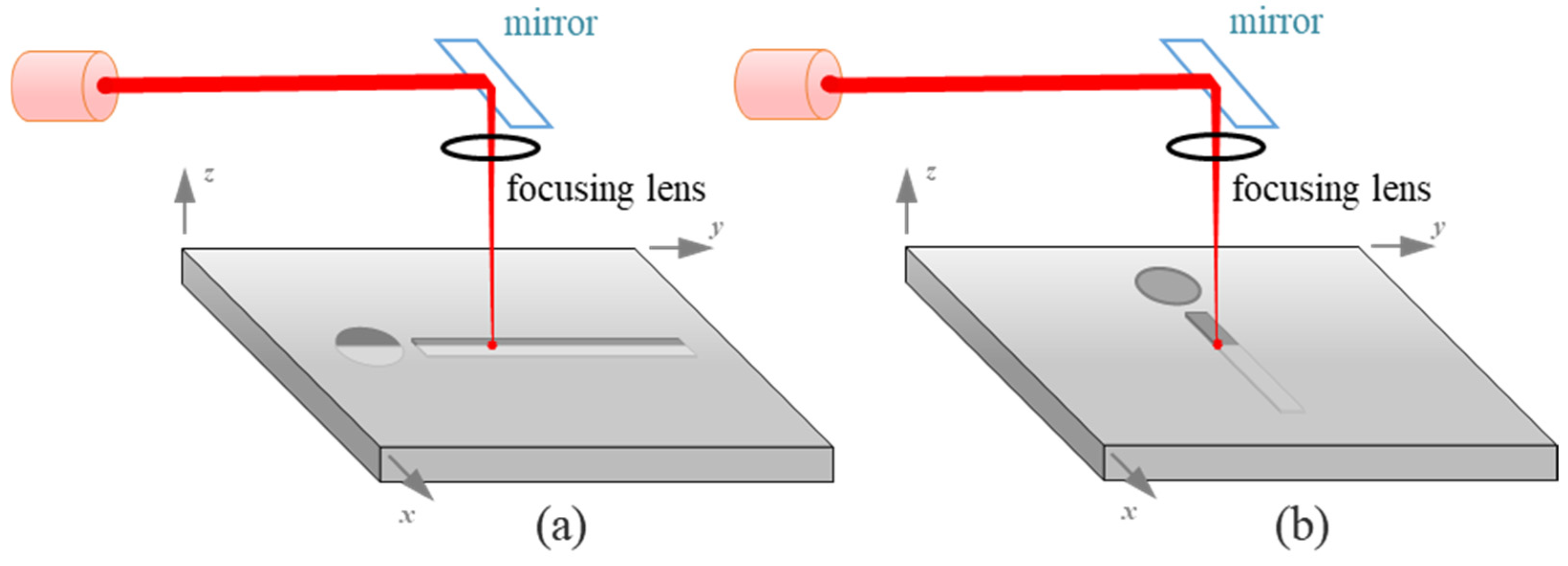
As shown in Figure 3, ablation patterns were oriented either (a) parallel or (b) perpendicular to the laser’s raster direction. Starting at the top-left of each subfigure, the laser beam (thick solid red line) was emitted from the laser source before being reflected off the mirror (blue) and focused on the surface of the specimen (gray) via the focusing lens (black). The mirror and the focusing lens were located on the carriage, which rapidly translated parallel to the y-direction to ablate a single raster. After completing a raster, the carriage translated a small distance in the positive x-direction before completing another raster. Specimens 2 and 4 were ablated with the major axes of the to-be-ablated rectangles parallel to the laser’s raster direction (cf. Figure 3a). Specimens 1 and 3 were ablated with the major axes of the to-be-ablated rectangles perpendicular to the laser’s raster direction (cf. Figure 3b). For all treatments, the laser beam was perpendicular to the to-be-ablated surface, i.e., the laser beam was parallel to the z-direction, as shown in Figure 3. The time to ablate a single specimen with eight treatments utilizing eight different sets of processing parameters and eight different ablation patterns was between 5 and 36 min. After ablation, specimens were chemically debound in a solvent and then thermally sintered per Desktop Metal guidelines (cf. [22]). Hence, laBMD is a laser ablation post-processing technique applied to BMD parts, not a new fabrication technology. For additional details, see Watson [44].
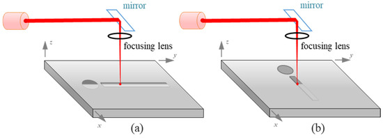
Figure 3.
Schematic showing ablation pattern relative to the laser rastering direction for (a) parallel and (b) perpendicular orientations.
2.1. Design of Experiments
A five-factor, two-level, i.e., 25, full-factorial design of experiments (DOE) was executed using the laser ablation factors and levels shown in Table 1. The selected factors address laser ablation, not BMD, process parameters. Values for low and high levels were determined based on qualitative experimentation prior to conducting the DOE. The treatment order was randomized by Minitab 19 [47], assuming blocking on the direction of laser travel.

Table 1.
Laser ablation factors and levels.
Response surfaces for four responses—average ablation depth D, ablated surface roughness Sq, the angle between ablated and non-ablated surfaces θ, and width at the bottom of the rectangular ablated region—were calculated in Minitab 19 [47], assuming an incomplete 2nd order response surface model of the form:
where y is the response of interest; , , and are the regression coefficients; , , and are the independent factors; = 5 is the number of factors; and is the error term. The exclusion of center points from the DOE means that quadratic terms of a single factor were undeterminable. Statistically significant hierarchical response surfaces for each of the three responses were then calculated via backward elimination [48], assuming α = 0.05 significance level. See Watson [44] for additional details.
2.2. Experimental Observations and Measurements
A Keyence VHX-7000 digital microscope Manufacturer: Keyence; City: Osaka; Country: Japan was utilized to obtain depth-composed optical and topological images to measure ablated depths, surface roughnesses, angles between ablated and non-ablated surfaces, and widths at the bottom and top of the ablated rectangles. The microscope utilized a VHX-E100 high-resolution objective lens, which at 100× magnification captures a 3.05 mm × 2.28 mm image. Using the high-resolution (4K Mode OFF) mode, the microscope’s VHX-7100 fully integrated head digitized 2880 pixels by 2160 pixels, resulting in an in-plane resolution of 1.1 µm per pixel [49]. The microscope’s 1 µm out-of-plane resolution was independent of magnification [49]. For to-be-examined features larger than the stationary 3.05 mm × 2.28 mm image capability, the part was translated via the microscope’s motorized stage, additional depth-composed images were captured, and images were stitched together.
2.2.1. Average Ablation Depth, D
The average ablation depth, D, represents the average ablated depth from a non-ablated region to an ablated region along the ablated rectangle’s major axis. As shown in Figure 4, the average ablated depth along the centerline, , equals the average depth from a line located on a non-ablated surface (yellow line) to a line located in the ablated region (cyan line). The yellow line was placed on the non-ablated surface sufficiently distant to avoid any heat-affected zone. Depth calculations were performed in the microscope’s VHX-H5M measurement module within the VHX Control System (Ver 18.12.04.0A Ver 01.00.00.02) [49]. As the ablated rectangular region may or may not have a uniform depth across the rectangle’s minor axis, average depths near the top and bottom of each rectangular region, and , were calculated. The average ablated depth for a treatment was calculated as .

Figure 4.
Ablated rectangular region of Treatment 1 showing (a) an optical image of the top view and (b) the measured depth along the rectangle’s major axis in a side view. In both views, the yellow line indicates the measured non-ablated height, and the cyan line indicates the measured ablated height along the centerline . In the side view, the red region represents the depth from the non-ablated height to the ablated height.
2.2.2. Surface Roughness of Ablated Regions, Sq
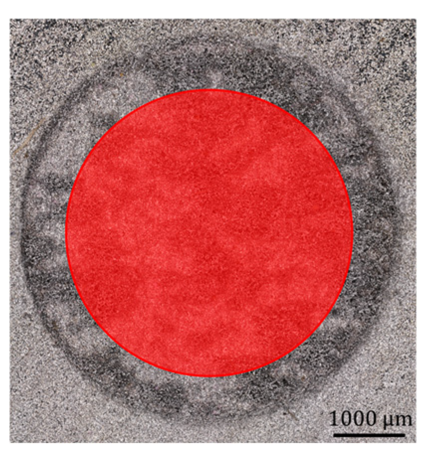
Surface roughness values were calculated via the microscope’s measurement software within a 4.0 mm diameter circular region of each treatment’s as-sintered 5.0 m diameter ablated circle. Figure 5 shows the centered positioning of the surface roughness measurement region (filled red circle) within the 5.0 mm diameter ablated region for Treatment 10. The 0.5 mm radial buffer between the measured region and the ablated region mitigates the influence of edge effects. Surface roughness Sq was calculated as the root mean square of height at each point in the measurement region [49].
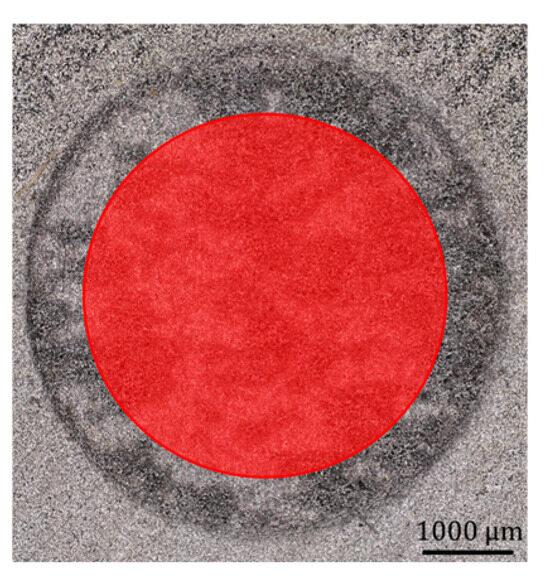
Figure 5.
Positioning of the 4.0 mm diameter surface roughness measurement region (red circle) within the 5.0 mm diameter circular ablated region for Treatment 10.
2.2.3. Angle Between Ablated and Non-Ablated Surfaces, θ
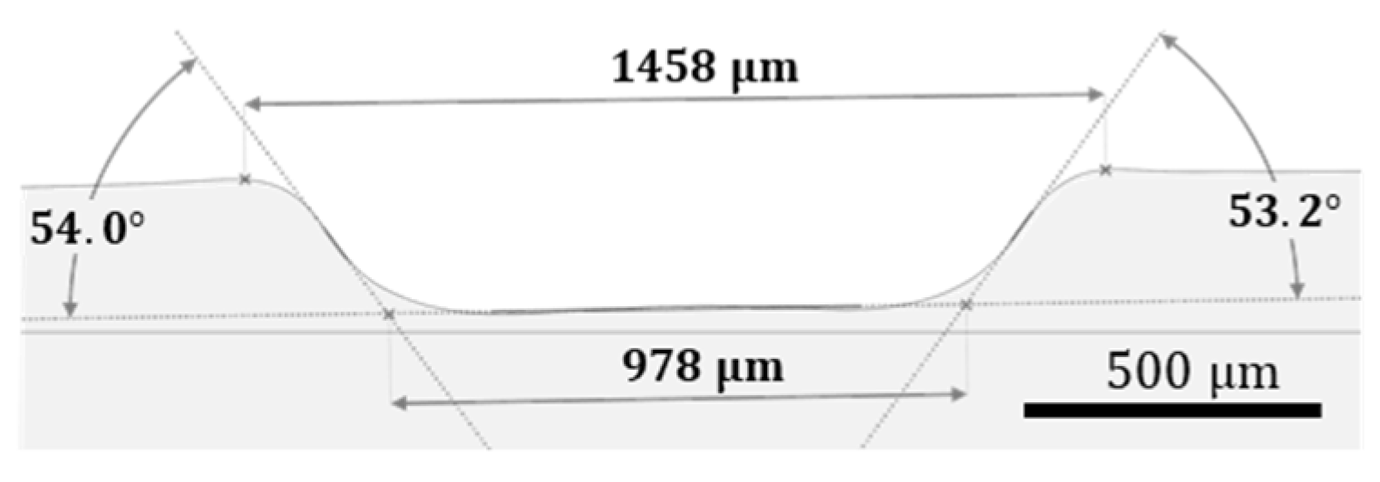
A cross-section of each treatment’s rectangular ablated region was created from 23 individual profiles taken at 0.5 mm intervals about the middle of the rectangular region, resulting in an 11 mm long region centered on the rectangle’s 30 mm long direction. The 23 cross-sections were averaged and analyzed via the microscope’s measurement software to calculate the maximum angle on the left and right side of that treatment’s average cross-section. The maximum calculated angles for the left and right cross-sections were then averaged to calculate the angle between ablated and non-ablated surfaces θ. For example, Figure 6 shows the average cross-section for Treatment 1 annotated with the microscope measurements of the 54.0° and 53.2° angles on the left and right side, respectively. Referring to Figure 6, the average angle θ for Treatment 1 is 53.6°, and the difference in angles Δθ for Treatment 1 is 0.8°.

Figure 6.
Average cross-section profile of the rectangular ablated region in the sintered state for Treatment 1 (T1). The gray-colored shading beneath the measured profile was added to aid visualization and, therefore, fails to show actual microstructure, such as intra- and inter-bead porosity.
2.2.4. Ablated Top Width, Wt, and Bottom Width, Wb
The widths at the top, Wt, and the bottom, Wb, of each treatment were calculated using the average cross-sections utilized to calculate θ and Δθ. The width at the top of each ablated rectangle was calculated as the Euclidean distance between two tangent points at the top of the average cross-section. As shown in Figure 6, Wt for Treatment 1 equals 1458 µm. The width at the bottom of the ablated rectangle was calculated as the Euclidean distance between two intersection points. The intersection points are defined as the intersection of the predominantly horizontal line at the bottom of the ablated rectangle and the lines defined by the left and right maximum angles. As shown in Figure 6, Wb for Treatment 1 equals 978 µm.
3. Results
Each of the four specimens was subjected to eight ablation treatments, resulting in a total of thirty-two treatments. To reduce variability during debinding and sintering, the four specimens were chemically debound in a single batch and then thermally sintered in a single batch. Optical images of the as-sintered specimens are shown in Figure 7.

Figure 7.
As-sintered Specimens 1−4 showing Treatments 1−32.
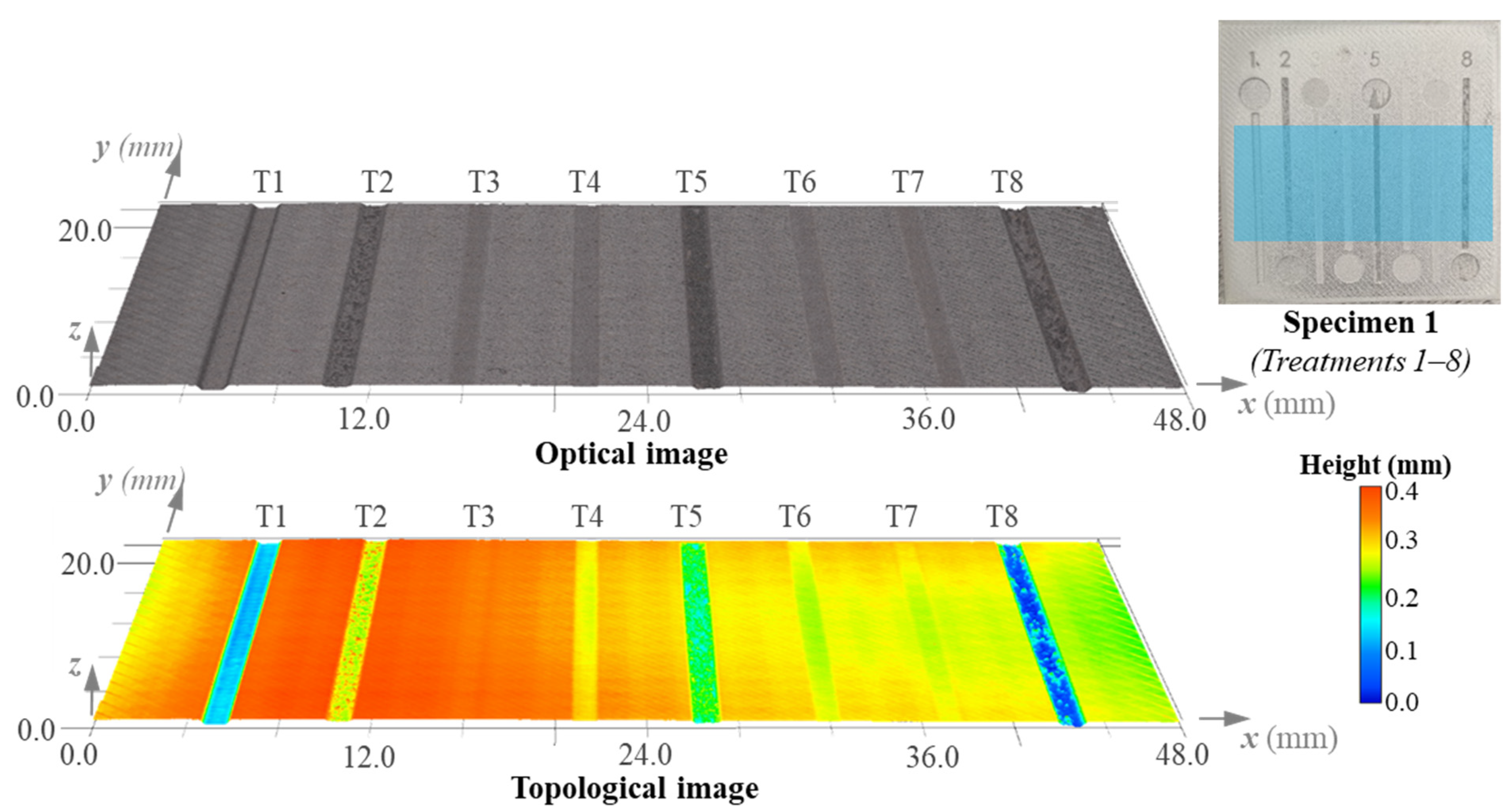
Figure 8 shows a qualitative comparison of channel topology for the mid-region of Treatments 1 through 8 on Specimen 1. In the upper-right corner of Figure 8, the blue-highlighted rectangle indicates the approximately 20 mm tall by 48 mm wide region shown in the optical and topological images. The optical and topological images in Figure 8 show the same surface.

Figure 8.
Optical (top) and topological (bottom) images showing a 20 mm long region of channels for Treatments 1–8 (i.e., Specimen 1). The approximate location of the imaged region is indicated by the blue-colored rectangle overlaid on Specimen 1 (cf. top-right corner).
Table 2 shows the corresponding treatment number, factors, levels, and numerical results for all treatments. For example, Treatment 1 was subjected to three passes of a 75% power laser traveling at a 50% speed perpendicular to the direction of the channel and having a 600 dpi resolution. The average depth in the as-sintered state of Treatment 1 was 229 µm, the average depth/pass was 76 µm, the surface roughness was 7.0 µm, the average angle was 53.6°, and the difference in angles was 0.8°.

Table 2.
Laser ablation treatment number (T#), processing parameters, and as-sintered depth, roughness, and ablation angles.
3.1. Ablated Depth, D
As shown in Table 2, average ablated depths ranged from 3 to 253 µm. Treatments 30, 1, and 12—all employing three laser passes at 75% power and 50% speed—resulted in the three deepest ablation depths of 253, 229, and 183 µm, respectively. In contrast, Treatments 22, 3, and 31—all employing one laser pass at 25% power and 100% speed—resulted in the three shallowest ablation depths of 3, 4, and 4 µm, respectively. Dividing each treatment’s ablation depth by the number of passes results in ablated depths/pass of 3 to 122 µm/pass.
Assuming up to second-order interaction terms and the five factors within a regression model (cf. Section 2.1), the regression equation for as-sintered ablated depth is as follows:
where is the regressed as-sintered depth in µm, d is the direction of laser travel with perpendicular directions coded as 1 and parallel directions coded as 0, s is the scanning speed in % (i.e., coded as “50” for 50% speed), p is the laser power in % (i.e., coded as “75” for 75% power), and n is the number of laser passes. The regression equation has an R2 = 0.784. It is interesting that for the factors and levels considered, the resolution r was statistically insignificant at α = 0.05.
Figure 9 shows the regressed average as-sintered depth as a function of measured as-sintered depth for all 32 treatments. Except for Treatments 1, 17, and 30, the regression equation predicts the depth within 50 µm, as shown by the dashed lines in Figure 9.
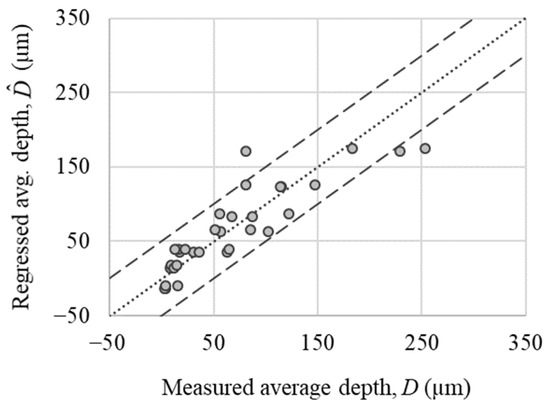
Figure 9.
Regressed average as-sintered depth as a function of measured average as-sintered depth. Perfect correlation is indicated by the dotted line. The dashed line above and below the dotted line indicate +50 and −50 µm offsets, respectively.
3.2. Surface Roughness, Sq
The regression equation for as-sintered surface roughness is as follows:
where is the regressed surface roughness in µm, r is the laser resolution in dpi, and d, s, p, and n were previously defined. The R2 = 0.768 for Equation (3). Figure 10 shows the regressed average sintered depth as a function of measured as-sintered depth for all 32 treatments. Except for Treatments 8, 17, and 30, regressed surface roughness values are within ±12 µm of the measured surface roughness values, as shown by the dashed lines in Figure 10.
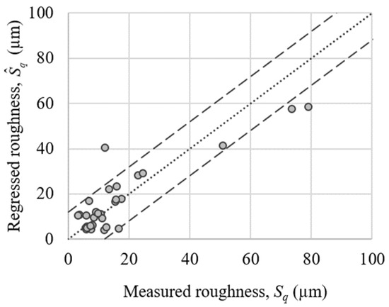
Figure 10.
Regressed as-sintered roughness as a function of measured as-sintered roughness. Perfect correlation is indicated by the dotted line. The dashed line above and below the dotted line indicate +12 and −12 µm offsets, respectively.
3.3. Average Angle Between Ablated and Non-Ablated Surfaces, θ
The regression equation for the average as-sintered angle between ablated and non-ablated surfaces in the rectangular region is as follows:
where is the regressed average angle between ablated and non-ablated surfaces in degrees, and d, s, p, n, and r were previously defined. The R2 = 0.941 for Equation (4). Figure 11 shows the regressed angle as a function of measured angle θ for all 32 treatments. Except for Treatments 10 and 11, all regressed angles are within 15° of the measured angles, as shown by the dashed lines in Figure 11. A maximum average angle θ of 68.2° was measured for Treatment 30, having three passes at 75% power and 50% speed parallel to rectangular ablation pattern at a 1200 dpi resolution.
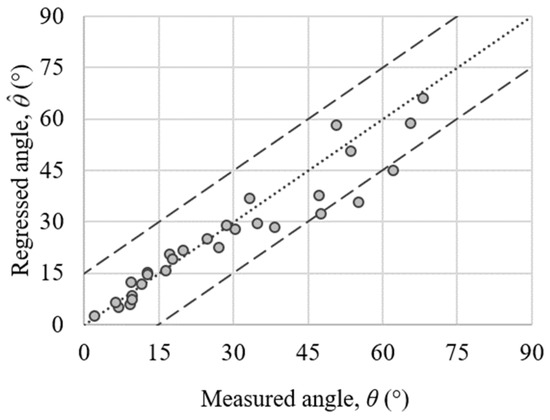
Figure 11.
Regressed as-sintered angle as a function of measured as-sintered angle. Perfect correlation is indicated by the dotted line. The dashed line above and below the dotted line indicate +15° and −15° offsets, respectively.
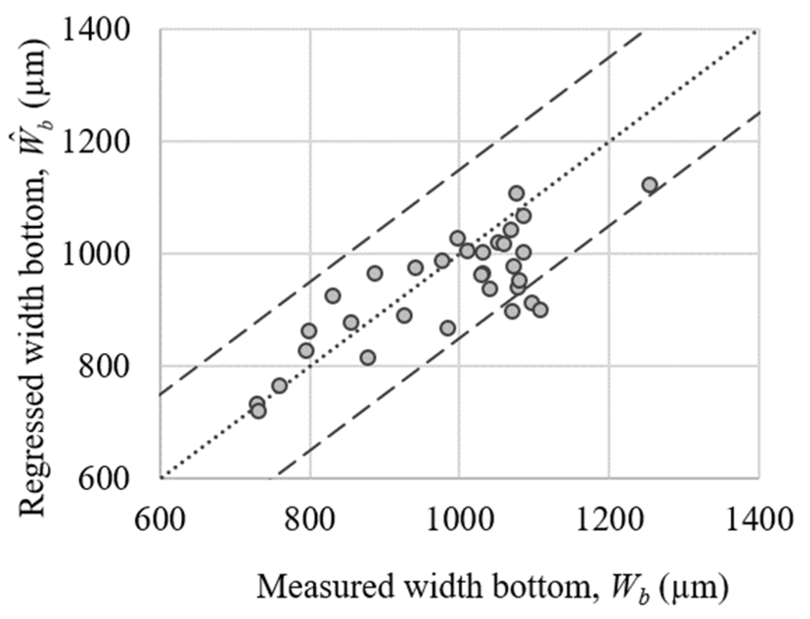
3.4. Ablated Width at Bottom of Rectangle, Wb
The regression equation for the as-sintered width at the bottom of the rectangular ablated region is as follows:
where is the regressed width at the bottom of the rectangular ablated region in µm, and d, s, p, n, and r were previously defined. The R2 = 0.756 for Equation (5). Figure 12 shows the regressed width as a function of measured Wb for all 32 treatments. Except for Treatments 9, 15, and 31, Equation (5) predictions are within 150 µm of the measured widths, as shown by the dashed lines in Figure 12.

Figure 12.
Regressed as-sintered width as a function of measured as-sintered width. Perfect correlation is indicated by the dotted line. The dashed line above and below the dotted line indicate +150 and −150 µm offsets, respectively.
For the design of more complex ablation patterns, it is important to note that and Wb are dependent upon laser direction d. For example, Wb for treatments having parallel laser directions was 164 µm wider, on average, than Wb for treatments having perpendicular laser directions. The 164 µm increase in width was statistically significant at α = 0.05 as determined by a two-sample t-test (p < 0.001). Recalling that parallel ablation patterns require less processing time, it is possible that heat-affected regions adjacent to vaporized regions have less time to dissipate heat. Hence, the finding that parallel laser directions result in wider widths suggests a temperature-dependent fluence ablation threshold and motivates the development of path-dependent numerical modeling.
3.5. D–Sq– θ Response Space
Responses in the D–Sq–θ space are shown in Figure 13, in which the (a–c) subfigures show paired responses in the θ–Sq, θ–D, and Sq–D planes. In Figure 13b,c, the ablated depth is normalized by the number of passes.

Figure 13.
D–Sq–θ response space showing the (a) θ–Sq, (b) θ–D/pass, (c) and Sq–D/pass planes. Treatment number is indicated via a number adjacent to each data point.
Figure 13 primarily serves as a design tool to identify feasible response combinations. For example, Figure 13a indicates a non-linear relationship between ablation angle θ and surface roughness Sq with ablation angles less than 70° regardless of surface roughness. Further, Figure 13c suggests that the ablation depth D/pass may be selected between 3 and 122 µm/pass while maintaining a surface roughness Sq ≤ 30 µm. See Watson [44] for additional details.
4. Discussion
Whereas prior studies of laser ablation of polymer–metallic composites determined machining depth as a function of scanning speed [41] and the effect of particle shape on ablation [42], this study quantifies the relation between laser ablation parameters and ablated geometries and surface finishes. For specific applications (e.g., molding surfaces for manufacturing microfluidic devices [50]), it is desirable to control all four studied responses: Wb, D, Sq, and θ. Of these, Wb and D are relatively easy to adjust. At the coarser 600 dpi resolution, Wb can spatially resolve 42 µm during green-state ablation. Assuming a 19.07% shrinkage, the spatial resolution in the as-sintered state is approximately 35 µm. The finer 1200 dpi resolution can resolve 21 and 18 μm in the green and as-sintered states, respectively. The depth D is similarly relatively easy to control by changing the number of passes.
In contrast, Sq and θ must be controlled by ablation processing parameters. Sq was predominantly influenced by resolution r, with r = 600 dpi resulting in smoother surfaces than those of r = 1200 dpi. For example, Treatments 1 and 17 had the same processing parameters, except for r = 600 dpi for Treatment 1 and r = 1200 dpi for Treatment 17. Treatment 1 (r = 600 dpi) had Sq = 7.0 μm, but Treatment 17 (r = 1200 dpi) had Sq = 73.6 μm. Whereas r dominated the response of Sq, n and p dominated the response of θ, with increasing n and p increasing θ. As examples, Treatments 1 and 6 had the same processing parameters, except for n and p. Treatment 1 (n = 3, p = 75%) had θ = 53.6°, and Treatment 6 (n = 1, p = 25%) had θ = 7.0°. Importantly, r had only a minor effect on θ, as demonstrated by Treatments 1 (r = 600 dpi) and 17 (r = 1200 dpi) having θ = 53.6° and θ = 50.7°, respectively, yet having otherwise the same processing conditions. The observation that Sq and θ are controllable by different processing parameters is critical to being able to tailor a laBMD process for an application.
Compared to the BMD process, the laBMD process has at least six demonstrated or anticipated advantages: (1) finer control of depth, (2) finer control of curvilinear in-plane features, (3) positive draft angles, (4) approximately ¼ of the manufacturing time of BMD’s finest-resolution printing while being able to produce finer features, (5) narrower widths for embossed features, and (6) an ability to tailor ablation processing parameters to have even more control on responses of interest.
Despite seeking an accurate and complete characterization of the effects of laser ablation on green-state BMD parts, some limitations exist. First, this work only examined the effects of laser ablating 17-4 PH green-state parts prior to solvent-based chemical debinding and thermal sintering. Other green-state composites and BMD material systems may have different constituents, constituent volume fractions, and absorption and thermal properties that require additional experimentation. Second, this work considers the ablation of relatively small regions at the top of 5.93 mm thick green-state parts. It is possible and likely that ablating a large surface area of a relatively thin part may require additional geometric considerations. For example, ablating a large percentage of the surface area may either release residual stresses or induce thermal stresses within the green-state part, resulting in part warpage. Reductions in green-state part thickness may exacerbate such effects.
5. Summary and Conclusions
This work demonstrated and characterized a laser-ablated bound metal deposition (laBMD) process in which conventional BMD parts were laser-ablated in the green state to create fine-scale features. The demonstrated process utilized a 60-watt CO2 Epilog Helix laser to ablate green-state 17-4 PH parts processed via a bound metal deposition (BMD). The laBMD process was characterized via a full-factorial design of experiments utilizing five factors, each having two levels: (1) number of laser passes (one pass, three passes), (2) laser power (25%, 75%), (3) scanning speed (50%, 100%), (4) direction of laser travel (perpendicular, parallel), and (5) laser resolution (600 dpi, 1200 dpi). The five-factor, two-level DOE resulted in a total of 32 treatments and considered four responses: ablated depth, ablated surface roughness, angle between ablated and non-ablated regions, and ablated width.
For the factors and levels considered, the as-sintered ablation depths/pass ranged from 3 and 122 µm/pass, the ablated surface roughness ranged from 3 to 79 µm, the angle between ablated and non-ablated regions ranged from 1° to 68°, and ablated widths ranged from 729 to 1254 µm. Each of the four responses of interest was regressed via backward elimination starting from an incomplete second-order response surface model to determine statistically significant terms. Results indicated that the five factors predict between 75 and 94% of the experimentally observed variation in the response for the factors and levels considered. Lastly, an examination of the D–Sq–θ response space provided a better understanding of the interplay among the responses of interest and indicated a non-linear θ–Sq relationship.
Author Contributions
Conceptualization, J.B. and B.D.E.; Data curation, A.W. and J.M.; Formal analysis, A.W.; Funding acquisition, J.B. and B.D.E.; Investigation, A.W. and J.M.; Methodology, A.W. and B.D.E.; Project administration, J.B.; Resources, J.B.; Software, A.W.; Supervision, M.R.-R. and B.D.E.; Validation, A.W. and J.M.; Visualization, A.W., J.M. and B.D.E.; Writing—original draft, A.W.; Writing—review and editing, A.W., M.R.-R. and B.D.E. All authors have read and agreed to the published version of the manuscript.
Funding
This research was funded by the Maine Technology Institute (MTI), grant number #CIP209, and the University of Maine’s Advanced Manufacturing Center (AMC). The APC was funded by the authors.
Data Availability Statement
The data are available within the paper.
Acknowledgments
The authors gratefully acknowledge the Desktop Metal support team for their technical support.
Conflicts of Interest
The authors declare no conflicts of interest.
Abbreviations
The following abbreviations are used in this manuscript:
| AM | Additive manufacturing |
| AMM | Additive manufacturing of metals |
| BMD | Bound metal deposition |
| DM | Desktop Metal |
| DOE | Design of experiments |
| dpi | Dots per inch |
| FM | Formative manufacturing |
| laBMD | Laser-ablated bound metal deposition (BMD) |
| SM | Subtractive manufacturing |
References
- ASTM 52900; Standard Terminology for Additive Manufacturing Technology—General Principles—Terminology. ASTM International: West Conshohocken, PA, USA, 2015.
- Li, M.; Du, W.; Elwany, A.; Pei, Z.; Ma, C. Metal binder jetting additive manufacturing: A literature review. J. Manuf. Sci. Eng. 2020, 142, 090801-1–090801-17. [Google Scholar] [CrossRef]
- Dass, A.; Moridi, A. State of the art in directed energy deposition: From additive manufacturing to materials design. Coatings 2019, 9, 418. [Google Scholar] [CrossRef]
- DebRoy, T.; Wei, H.L.; Zuback, J.S.; Mukherjee, T.; Elmer, J.W.; Milewski, J.O.; Beese, A.M.; Wilson-Heid, A.; De, A.; Zhang, W. Additive manufacturing of metallic components—Process, structure and properties. Prog. Mater. Sci. 2018, 92, 112–224. [Google Scholar] [CrossRef]
- Gonzalez-Gutierrez, J.; Cano, S.; Schuschnigg, S.; Kukla, C.; Sapkota, J.; Holzer, C. Additive manufacturing of metallic and ceramic components by the material extrusion of highly-filled polymers: A review and future perspectives. Materials 2018, 11, 840. [Google Scholar] [CrossRef] [PubMed]
- Bhavar, V.; Kattire, P.; Patil, V.; Khot, S.; Gujar, K.; Singh, R. A review on powder bed fusion technology of metal additive manufacturing. In Additive Manufacturing Handbook, 1st ed.; Badiru, A.B., Valencia, V.V., Badiru, A.B., Liu, D., Hartsfield, C.R., Eds.; CRC Press: Boca Raton, FL, USA, 2017; pp. 251–253. [Google Scholar]
- Gibson, I.; Rosen, D.W.; Stucker, B. Sheet lamination processes. In Additive Manufacturing Technologies, 2nd ed.; Gibson, I., Rosen, D.W., Stucker, B., Eds.; Springer: Boston, MA, USA, 2015; pp. 219–244. [Google Scholar] [CrossRef]
- Srivastava, M.; Rathee, S.; Maheshwari, S.; Noor Siddiquee, A.; Kundra, T.K. A review on recent progress in solid state friction based metal additive manufacturing: Friction stir additive techniques. Crit. Rev. Solid State Mater. Sci. 2019, 44, 345–377. [Google Scholar] [CrossRef]
- Yin, S.; Cavaliere, P.; Aldwell, B.; Jenkins, R.; Liao, H.; Li, W.; Lupoi, R. Cold spray additive manufacturing and repair: Fundamentals and applications. Addit. Manuf. 2018, 21, 628–650. [Google Scholar] [CrossRef]
- Chen, W.; Thornley, L.; Coe, H.G.; Tonneslan, S.J.; Vericella, J.J.; Zhu, C.; Duoss, E.B.; Hunt, R.M.; Wight, M.J.; Apelian, D.; et al. Direct metal writing: Controlling the rheology through microstructure. Appl. Phys. Lett. 2017, 110, 094104. [Google Scholar] [CrossRef]
- Matthews, M.J.; Guss, G.; Drachenberg, D.R.; Demuth, J.A.; Heebner, J.E.; Duoss, E.B.; Kuntz, J.D.; Spadaccini, C.M. Diode-based additive manufacturing of metals using an optically-addressable light valve. Opt. Express. 2017, 25, 11788–11800. [Google Scholar] [CrossRef]
- Tepylo, N.; Huang, X.; Patnaik, P.C. Laser-based additive manufacturing technologies for aerospace applications. Adv. Eng. Mater. 2019, 21, 1900617. [Google Scholar] [CrossRef]
- Wu, T.; Jahan, S.A.; Kumaar, P.; Tovar, A.; El-Mounayri, H.; Zhang, Y.; Zhang, J.; Acheson, D.; Brand, K.; Nalim, R. A framework for optimizing the design of injection molds with conformal cooling for additive manufacturing. Procedia Manuf. 2015, 1, 404–415. [Google Scholar] [CrossRef]
- Morgan, H.D.; Levatti, H.U.; Sienz, J.; Gil, A.J.; Bould, D.C. GE jet engine bracket challenge: A case study in sustainable design. KES Trans. Sustain. Des. Manuf. 2014, 1, 95–107. [Google Scholar]
- Deradjat, D.; Minshall, T. Implementation of rapid manufacturing for mass customization. J. Manuf. Technol. Manag. 2017, 28, 95–121. [Google Scholar] [CrossRef]
- Kok, Y.; Tan, X.P.; Wang, P.; Nai, M.L.S.; Loh, N.H.; Liu, E.; Tor, S.B. Anisotropy and heterogeneity of microstructure and mechanical properties in metal additive manufacturing: A critical review. Mater. Des. 2018, 139, 565–586. [Google Scholar] [CrossRef]
- Das, S.; Bourell, D.L.; Babu, S.S. Metallic materials for 3D printing. MRS Bull. 2016, 41, 729–741. [Google Scholar] [CrossRef]
- Milewski, J.O. Additive Manufacturing of Metals, 1st ed.; Springer International Publishing: Cham, Switzerland, 2017; pp. 35–48. [Google Scholar] [CrossRef]
- Ngo, T.D.; Kashani, A.; Imbalzano, G.; Nguyen, K.T.Q.; Hui, D. Additive manufacturing (3D printing): A review of materials, methods, applications and challenges. Compos. Part B 2018, 143, 172–196. [Google Scholar] [CrossRef]
- Turner, B.N.; Gold, S.A. A review of melt extrusion additive manufacturing processes: II. Materials, dimensional accuracy, and surface roughness. Rapid Prototyp. J. 2015, 21, 250–261. [Google Scholar] [CrossRef]
- Watson, A.; Belding, J.; Ellis, B.D. Characterization of 17-4 PH processed via bound metal deposition (BMD). In Proceedings of the TMS 2020 149th Annual Meeting & Exhibition Supplemental Proceedings, San Diego, CA, USA, 23–27 February 2020; The Minerals, Metals & Materials Society, Ed.; Springer International Publishing: Cham, Switzerland, 2020; pp. 205–216. [Google Scholar] [CrossRef]
- Desktop Metal. BMD Design Guide. Available online: https://www.desktopmetal.com/uploads/20230912_R03_Studio-System-BMD-Design-Guide_2023-09-13-123253_cupr.pdf (accessed on 1 December 2021).
- German, R. Powder Metallurgy & Particulate Materials Processing, 1st ed.; Metal Powder Industry: Princeton, NJ, USA, 2005. [Google Scholar]
- Olevsky, E.A. Theory of sintering: From discrete to continuum. Mater. Sci. Eng. R Rep. 1998, 23, 41–100. [Google Scholar] [CrossRef]
- Banerjee, S.; Joens, C.J. Debinding and sintering of metal injection molding (MIM) components. In Handbook of Metal Injection Molding, 1st ed.; Heaney, D.F., Ed.; Woodhead: Cambridge, UK, 2012; pp. 133–180. [Google Scholar]
- Desktop Metal. Fabricate. Available online: https://fab.desktopmetal.com (accessed on 1 December 2021).
- Ravi-Kumar, S.; Lies, B.; Lyu, H.; Qin, H. Laser ablation of polymers: A review. Procedia Manuf. 2019, 34, 316–327. [Google Scholar] [CrossRef]
- Ahmed, N.; Darwish, S.; Alahmari, A.M. Laser ablation and laser-hybrid ablation processes: A review. Mater. Manuf. Process. 2016, 31, 1121–1142. [Google Scholar] [CrossRef]
- Hoffman, J. The effect of recoil pressure in the ablation of polycrystalline graphite by a nanosecond laser pulse. J. Phys. D Appl. Phys. 2015, 48, 235201. [Google Scholar] [CrossRef]
- Förster, D.; Bui, D.A.; Onuseit, V.; Weber, R.; Graf, T. Energy transfer mechanisms during laser pulsed processing of metals. In Proceedings of the Lasers in Manufacturing Conference, München, Germany, 22–25 June 2015. [Google Scholar]
- Raciukaitis, G.; Gedvilas, M. Processing of polymers by UV picosecond lasers. In Proceedings of the ICALEO 2005: 24th International Congress on Laser Materials Processing and Laser Microfabrication, Miami, FL, USA, 31 October–3 November 2005; p. M403. [Google Scholar] [CrossRef]
- Vora, H.D.; Santhanakrishnan, S.; Harimkar, S.P.; Boetcher, S.K.S.; Dahotre, N.B. One-dimensional multipulse laser machining of structural alumina: Evolution of surface topography. Int. J. Adv. Manuf. Technol. 2013, 68, 69–83. [Google Scholar] [CrossRef]
- Galasso, G.; Kaltenbacher, M.; Tomaselli, A.; Scarpa, D. A unified model to determine the energy partitioning between target and plasma in nanosecond laser ablation of silicon. J. Appl. Phys. 2015, 117, 123101. [Google Scholar] [CrossRef]
- Cadot, G.B.J.; Axinte, D.A.; Billingham, J. Continuous trench, pulsed laser ablation for micro-machining applications. Int. J. Mach. Tools Manuf. 2016, 107, 8–20. [Google Scholar] [CrossRef]
- Li, X.; Guan, Y. Theoretical fundamentals of short pulse laser–metal interaction: A review. Nanotechnology Prec. Eng. 2020, 3, 105–120. [Google Scholar] [CrossRef]
- Förster, D.J.; Jäggi, B.; Michalowski, A.; Neuenschwander, B. Review on experimental and theoretical investigations of ultra-short pulsed laser ablation of metals with burst pulses. Mater. 2021, 14, 3331. [Google Scholar] [CrossRef]
- Gopal, P.M.; Kavimani, V.; Gupta, K.; Marinkovic, D. Laser-based manufacturing of ceramics: A review. Micromachines 2023, 14, 1564. [Google Scholar] [CrossRef] [PubMed]
- Butkutė, A.; Jonušauskas, L. 3D manufacturing of glass microstructures using femtosecond laser. Micromachines 2021, 12, 499. [Google Scholar] [CrossRef]
- Obilor, A.F.; Pacella, M.; Wilson, A.; Silberschmidt, V.V. Micro-texturing of polymer surfaces using lasers: A review. Int. J. Adv. Manuf. Tech. 2022, 120, 103–135. [Google Scholar] [CrossRef]
- Lambiase, F.; Genna, S.; Leone, C. Laser finishing of 3D printed parts produced by material extrusion. Opt. Lasers Eng. 2020, 124, 105801. [Google Scholar] [CrossRef]
- Slocombe, A.; Li, L. Laser ablation machining of metal/polymer composite materials. Appl. Surf. Sci. 2000, 154–155, 617–621. [Google Scholar] [CrossRef]
- Slocombe, A.; Taufik, A.; Li, L. Diode laser ablation machining of 316L stainless steel powder/polymer composite material: Effect of powder geometry. Appl. Surf. Sci. 2000, 168, 17–20. [Google Scholar] [CrossRef]
- Dessault Systèmes SolidWorks 2020. Available online: https://www.solidworks.com/ (accessed on 1 October 2021).
- Watson, A. Development and Characterization of Bound Metal Deposition Including Laser Ablation. Master’s Thesis, University of Maine, Orono, ME, USA, May 2022. [Google Scholar]
- Epilog Laser. Owner’s Manual for Epilog Mini/Helix—Model 8000; Epilog Laser: Golden, CO, USA, 2009. [Google Scholar]
- Sengdara, K. (Epilog, Golden, CO, USA). Personal communication, 2021.
- Minitab 19. Available online: https://www.minitab.com/ (accessed on 1 October 2021).
- Noordin, M.Y.; Venkatesh, V.C.; Sharif, S.; Elting, S.; Abdullah, A. Application of response surface methodology in describing the performance of coated carbide tools when turning AISI 1045 steel. J. Mater. Process. Technol. 2004, 145, 46–58. [Google Scholar] [CrossRef]
- Keyence. VHX-7000 Series Digital Microscope Catalog; Keyence: Osaka, Japan, 2019. [Google Scholar]
- Boutiette, A.L.; Toothaker, C.; Corless, B.; Boukaftane, C.; Howell, C. 3D printing direct to industrial roll-to-roll casting for fast prototyping of scalable microfluidic systems. PLoS ONE 2020, 15, e0244324. [Google Scholar] [CrossRef]
Disclaimer/Publisher’s Note: The statements, opinions and data contained in all publications are solely those of the individual author(s) and contributor(s) and not of MDPI and/or the editor(s). MDPI and/or the editor(s) disclaim responsibility for any injury to people or property resulting from any ideas, methods, instructions or products referred to in the content. |
© 2025 by the authors. Licensee MDPI, Basel, Switzerland. This article is an open access article distributed under the terms and conditions of the Creative Commons Attribution (CC BY) license (https://creativecommons.org/licenses/by/4.0/).


