Article

Thermal Modelling of Metals and Alloys Irradiated by Pulsed Electron Beam: Focus on Rough, Heterogeneous and Multilayered Materials

by
Andrea Lucchini Huspek
1,*,
Valentina Mataloni
1,
Ali Mohtashamifar
2,
Luca Paterlini
1 and
Massimiliano Bestetti
1
1
Department of Chemistry, Materials and Chemical Engineering “Giulio Natta”, Politecnico di Milano, Via Luigi Mancinelli 7, 20131 Milano, Italy
2
Institute of Condensed Matter Chemistry and Technologies for Energy, National Research Council, Corso Stati Uniti 4, 35127 Padova, Italy
*
Author to whom correspondence should be addressed.
J. Manuf. Mater. Process. 2025, 9(4), 130; https://doi.org/10.3390/jmmp9040130
Submission received: 22 February 2025 / Revised: 24 March 2025 / Accepted: 11 April 2025 / Published: 15 April 2025
(This article belongs to the Special Issue New Trends in Precision Machining Processes)

Abstract

:
Low-Energy High-Current Electron Beam (LEHCEB) is an innovative vacuum technology employed for the surface modification of conductive materials. Surface treatments by means of LEHCEB allow the melting and rapid solidification of a thin layer (up to ~10 μm) of material. The short duration of each pulse (2.5 μs) allows for the generation of high thermal rates, up to 109 K/s. Due to the peculiar features of LEHCEB source, in situ temperature monitoring inside the vacuum chamber is unfeasible, even with the most rapid IR pyrometers available on the market. Therefore, multiphysics simulations serve as a tool for predicting and assessing the thermal effects induced by electron beam irradiation. COMSOL Multiphysics was employed to study the thermal behaviour of metals and alloys at the sub-microsecond time scale by implementing both experimental power time profiles and semi-empirical electron penetration functions. Three case studies were considered: (a) 17-4 PH steel produced by Binder Jetting, (b) biphasic Al-Si13 alloy, and (c) Magnetron Sputtering Nb films on Ti substrate. The influence on the thermal effects of electron accelerating voltage and number of pulses was investigated, as well as the role of the physicochemical properties of the materials.

1. Introduction

Low-Energy High-Current Electron Beam (LEHCEB) is an innovative vacuum technology employed for the surface modification of conductive materials. A pulsed electron beam is generated from a Cu cathode by applying an accelerating voltage of 10–30 kV, transported through a Plasma-Filled Diode (PFD) generated from the Ar working gas, and directed toward the target by external solenoids [1]. The wide area (50 cm2) electron beam has a very short pulse duration (2–4 μs) and induces drastic modifications in a thin surface layer (up to approximately 10 μm) of the target material, causing strong out-of-equilibrium transformations in the microstructure [2]. Formation of metastable crystalline phases, homogenization of the chemical composition, and removal of second phases and impurities are expected after LEHCEB surface modification [3]. Since the pulse duration is extremely short and the generated thermal rate is considerably high (109 K/s), the in situ monitoring of the sample temperature is not possible by employing the fastest IR pyrometers available on the market. For this reason, multiphysics simulations are a viable tool to predict and estimate the thermal effects induced during and after electron beam irradiation. At the same time, simulations may be used to test hypotheses before conducting experiments, as they can help to identify critical factors and allow the systematic variation in parameters to assess their impact on the outcomes. Computational models dealing with LEHCEB irradiation were developed to describe the non-stationary thermal and stress fields occurring in the target material. The calculation of thermal effects induced by LEHCEB is carried out by solving an inhomogeneous, nonstationary heat equation with a volumetric heat source. Such models are based on three fundamental hypotheses, which were adopted in the present work as well [4,5]: the target is homogeneous in its physical and chemical properties, the energy release is uniform over the transversal beam cross section, and the diameter of the electron beam is much larger than the dimension of the heated region due to heat conduction within the time of observation. Markov et al. calculated the influence of the Cr film thickness (on Cu substrates) on the melting threshold of the system [6], modelled the molten depth achievable by varying the deposition strategy in the Ni-Al system [7], and investigated the melt lifetime of the Cr-Zr system by varying the applied energy density [8]. Following the same approach, they showed that the composition of surface alloys formed by thin films Magnetron Sputtering deposition and Low-Energy High-Current Electron Beam liquid mixing can be estimated prior to synthesis [9]. Shepel et al. studied the thermal behaviour of a MnS inclusion in AISI 316L, showing that the radical difference between the thermal properties of the second phase and of the metal matrix determines a large overheating of MnS [10]. In the present work, COMSOL Multiphysics was employed to study the thermal behaviour of metals and alloys at the sub-microsecond time scale. The implementation of experimental power profiles was accompanied by a set of theoretical functions to take into account electron penetration into the material. Unlike other cases available in the literature, in this study, the modelling is performed starting from real micrographs of the metallic systems considered, allowing us to study their thermal behaviour in detail. COMSOL Multiphysics is an advanced simulation software for modelling several physical phenomena, including heat transfer, fluid dynamics, and structural mechanics. It is widely employed in industries as well as in academic research and its multiphysics capabilities allow for the coupling of various processes within a single simulation. Incorporating simulative approaches offers significant advantages for electron beams in industrial applications. By providing detailed insights into the thermal behaviour during materials treatment, these models enable optimisation of process parameters [11] for widely employed applications of electron beams such as welding and additive manufacturing [12]. Thermal calculations can help to identify the most influential variables, hence guiding the design of experiments or industrial processes, reducing the related time and costs. Kurashkin et al. employed COMSOL Multiphysics to model the temperature distribution in electron beam welded joints for AMG-6 and VT-14 alloys in different operating modes [13]. Ansari et al. performed a multiphysics simulation of the different phenomena occurring between the energy source and powders during the Selective Laser Melting of AISI 316L, modelling the variation in surface temperature with respect to the scanning velocity and diameter of the laser spot [14]. Mayi et al. simulated the keyhole dynamics in static and dynamic laser welding, accounting for the laser trapping effect during the molten pool growth [15] as well as the formation of a laser-induced gas plume with experimental confirmation of the predicted behaviour [16]. Darif et al. investigated the modelling of Si Nanosecond Laser Annealing, obtaining detailed information about the surface temperature profile as a function of laser fluence, while taking into account the heat source distribution along the depth of the sample [17]. The present research aims to calculate the thermal fields induced by Low-Energy High-Current Electron Beam in rough (Binder Jetting printed 17-4 PH steel), heterogeneous (biphasic Al-Si13 alloy), and multilayered (Nb film deposited on Ti substrate) systems.

2. Materials and Methods

COMSOL Multiphysics (version 6.1) was employed to calculate the temperature fields induced into a metallic sample by a Low-Energy High-Current Electron Beam. A heat balance equation (Equation (1)) was processed using a Backward Differentiation Formula method with strict time stepping (0.1 μs) and an implicit solver type. Moreover, specific boundary and initial conditions were applied to model LEHCEB effects.
d z ρ C p T t + d z ρ C p u · T + · q = d z Q + q 0 + d z Q t e d
where dz represents the geometry thickness along the third dimension, ρ is the density, Cp is the specific heat capacity, u is the fluid velocity vector, ∇T is the thermal gradient, q is a heat flux (W/m2), Q is a heat source (W/m3), q0 is an inward heat flux, and Qted is the thermoelastic dumping. The heat capacity was implemented as a function of the body temperature. Ambient parameters and other relevant values employed for the simulation are reported in Table 1.
Heat conduction was modelled employing Equation (2), where k is the thermal conductivity. As with the heat capacity, thermal conductivity was introduced as a function of temperature using data from the literature and databases.
q = d z k T
Heat convection was modelled through Equations (3) and (4), where n represents the normal vector toward the exterior, h is the heat transfer coefficient, and Tamb is the environment temperature. The heat transfer coefficient depends on T, Tamb, and the Rayleigh number (Ra).
n · q = d z q c
q c = h   (   T a m b T )
Heat irradiation was computed through Equations (5) and (6), where ε is the surface emissivity of a polished metal surface, and σ is the Stefan–Boltzmann constant.
n · q = d z q r
q r = ε σ   ( T a m b 4 T 4 )
The melting transition was modelled through the Apparent Heat Capacity Method, according to Equations (7)–(10). The software gradually modifies the thermal properties of the solid (θ1) into the ones of the liquid (θ2). The melting latent heat (L1→2) is then introduced at the melting temperature.
C p = θ 1 C p , 1 + θ 2 C p , 2 + L 1 2 α m T
α m = 1 2     θ 2 θ 1   θ 2 + θ 1
θ 1 + θ 2 = 1
k = θ 1 k 1 + θ 2 k 2
The boiling transition was modelled by deforming the mesh of the geometry. For this purpose, a boundary condition in the form of a heat flux (Equation (12)) was applied to the irradiated surface. The heat transfer coefficient (he) is null for every temperature below the boiling point (Te). Instead, above the boiling point, he has a slope of 109 W/m2K2, that the temperature of the liquid cannot markedly exceed the evaporation point. The evaporation velocity (Ve) was computed according to Equation (13), where Le is the latent heat of evaporation. The boiling point of metals was adjusted considering the working pressure (1.8 × 10⁻⁴ torr) during electron beam treatments.
n · q = d z q e
q e = h e (   T T e )
V e = q e ρ L e
The energy density is not delivered uniformly during an electron beam pulse but rather follows an oscillating trend. For this reason, experimental power profiles recorded by an oscilloscope (Tektronix-TBS 1052-EDU 50 MHz, Tektronix, Inc., Beaverton, OR, USA) were implemented in the model, as shown in Figure 1. The integral of the curves represents the energy density delivered by the electron beam. Instead, multiple pulse treatments were modelled by employing a rectangular power profile (i.e., ρ(w)EB) to save computational cost. A combination of Event nodes, represented by Equations (14)–(16), was used to model the pulsed irradiation. For a generic n-th pulse, the power input (μ) is turned on for 2.5 µs (τp) while the shut-down is approximated with the reciprocal of the repetition frequency (ωp) as the period is six orders of magnitude longer than the pulse duration.
u t i ( n ) = 0   u t i ( n ) = ρ ( w ) E B   u t f ( n ) = ρ ( w ) E B u t f ( n ) + = 0
t f ( n )   t i ( n )   = τ p
t f n + t i n + 1 1 ω p
An accurate calculation of the thermal effects along the depth of the material requires taking into account the electron energy losses. In fact, at 15–30 kV, electrons that collide with the metal release their energy to the material in the first micrometres. To model this phenomenon, the following semi-empirical function was used [4]:
f z / r = 1.4   e x p [ 2 z / r 0.66 2 ]
r = C ( E 0 / e ) 3 / 2 ρ
where z is the depth, C is a constant equal 10−17/2 kg m−2 V−3/2, E0 is the initial energy of electrons, and e is the electron charge. Figure 2 shows the in-depth electron energy distribution for different materials. All the curves have the same subtended area, which corresponds to the experimentally measured energy density (Ep). For heavy metals, the energy is released close to the surface, whereas light metals distribute the energy for a few micrometres. As a consequence, upon LEHCEB irradiation, a higher surface peak temperature is expected on Cu and Cr rather than on Al and Si.
Scanning Electron Microscopy (SEM) was performed employing a Zeiss EVO 50 (Zeiss Microscopy, Jena, Germany) equipped with a Bruker Quantax spectrometer (Bruker Corporation, Billerica, MA, USA) for Energy Dispersive X-Ray Spectroscopy (EDX). Optical Microscopy (OM) was carried out by means of a Leica DM LM (Leica Microsystems, Wetzlar, Germany) equipped with a Leica DFC290 camera.

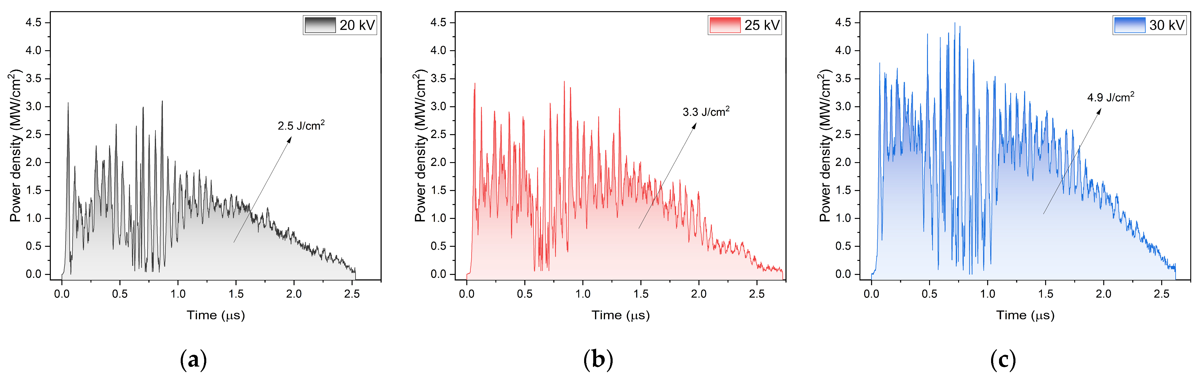
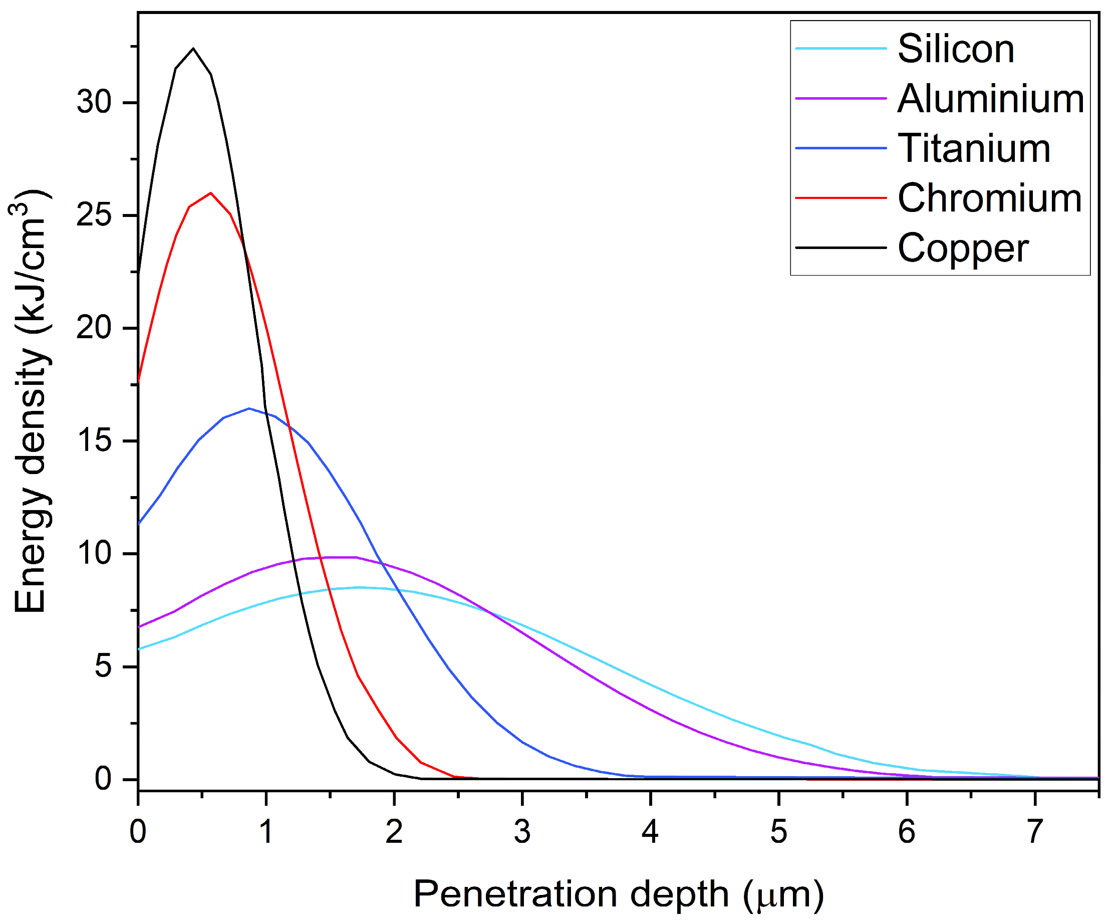
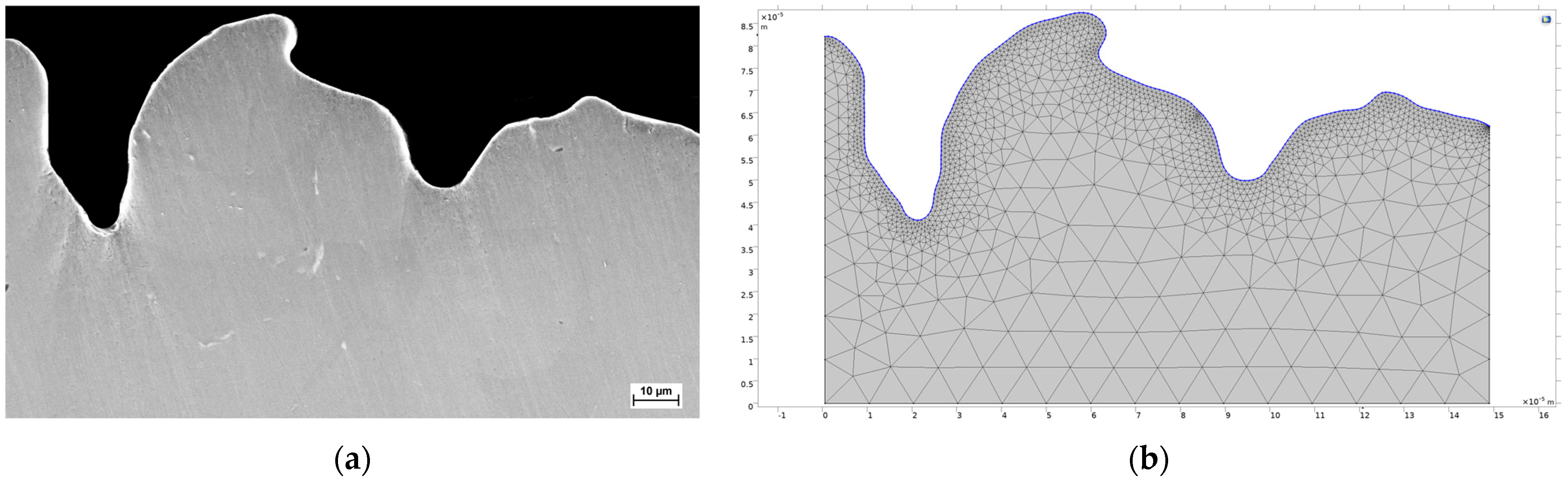
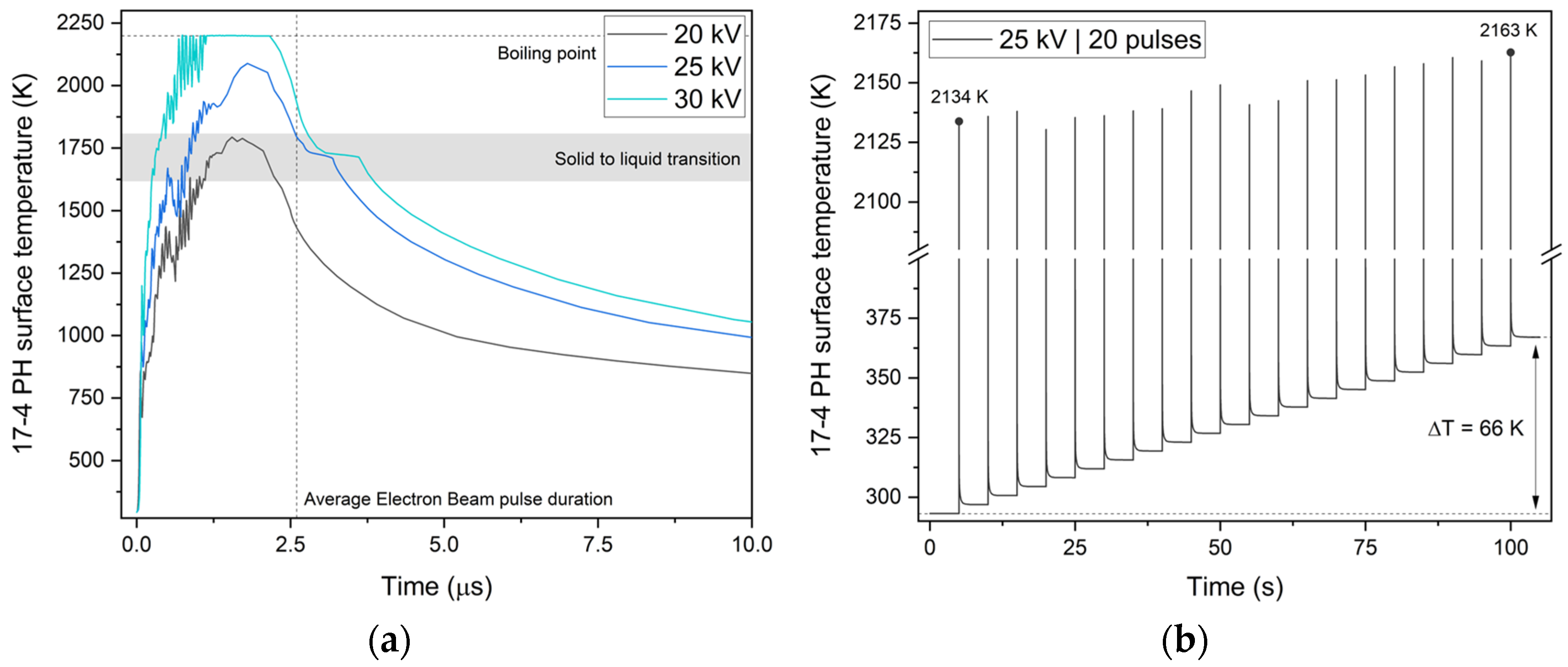
3. Results and Discussion

3.1. 17-4 PH Steel Produced by Metal Binder Jetting
The SEM cross section of a 17-4 PH component produced by metal Binder Jetting (BJ) is reported in Figure 3a. The typical morphology of BJ components characterised by dimples and asperities, can be appreciated from the micrograph. Figure 3b shows the corresponding meshed geometry employed in COMSOL Multiphysics for the thermal calculations. For 17-4 PH steel, the relevant temperature-dependent properties (i.e., thermal conductivity and specific heat capacity) were taken from [18]. The real density of the workpiece (96.7%) was measured by the Archimedes method, while the boiling point of the steel was qualitatively lowered to account for the working pressure within the vacuum chamber. Figure 4a shows the sub-microsecond variation in the metal surface temperature during a 20, 25, or 30 kV pulse. Temperature is quickly raised as soon as the pulse starts, resulting in a heating rate of more than 109 K/s for all three cases considered. The 20 kV treatment is the mildest one since the heating rate, as well as the surface temperature, depends on the energy density delivered by the electron gun. Nevertheless, a short time interval in which the material is in the liquid state can be observed between 1.2 and 2.1 µs. The maximum surface temperature at 20 and 25 kV is reached at 1.7 and 1.8 µs, respectively. At 30 kV, the material reaches the boiling point after 0.8 µs and the molten metal is present on the surface for around 3.3 µs. As a consequence, the persistence for a longer time of the liquid metal on the surface is observed at high accelerating voltage and this in turn favours a decrease in the roughness, as shown in [19]. In the early stages of the pulse, the rapid fluctuation of the power input, reported in Figure 1, causes an oscillation of the surface temperature. Instead, during the free cooling stage of the material, the temperature profile is smoother and more regular. At 25 and 30 kV, the molten volume is large enough to enable proper observation of the small temperature plateau associated with the solidification of the steel. In fact, heat is released during the phase transition, thus slowing down the decrease in temperature. The cooling rate is about one order of magnitude lower than the heating one, being around 108 K/s. Nevertheless, this cooling rate is much faster than the one of conventional heat treatments and leads to the formation of the out-of-equilibrium crystalline microstructures commonly found in LEHCEB-treated materials. Figure 4b shows the surface temperature profile of a sample treated with 20 pulses at 25 kV, with 0.2 Hz of pulse repetition frequency. The aim of calculating temperature evolution on a longer time scale is to understand how much the temperature can build up in the sample and how this affects the following pulses. From an experimental point of view, the use of a high number of electron beam pulses is usually exploited to homogenise the effects of the surface treatment. The geometry for this case was enlarged (H 0.15 × W 0.15 × D 2.5 mm3) to allow proper heat conduction from the surface to the bulk material. The outcome of the numerical calculation of a multiple pulse experiment is much more geometry-sensitive rather than the calculation of a single pulse irradiation. A thin lamina (<0.2 mm) experiences a more pronounced temperature evolution with respect to a thick block (>5 mm). A mild increase of 29 K in the maximum temperature after the last pulse with respect to the first one was observed. Instead, the minimum temperature in between pulses was increased by 66 K. This asymmetry is likely related to the increase in the metal thermal diffusivity with temperature (α(T) = k(T)/ρ (T) × CP(T)).

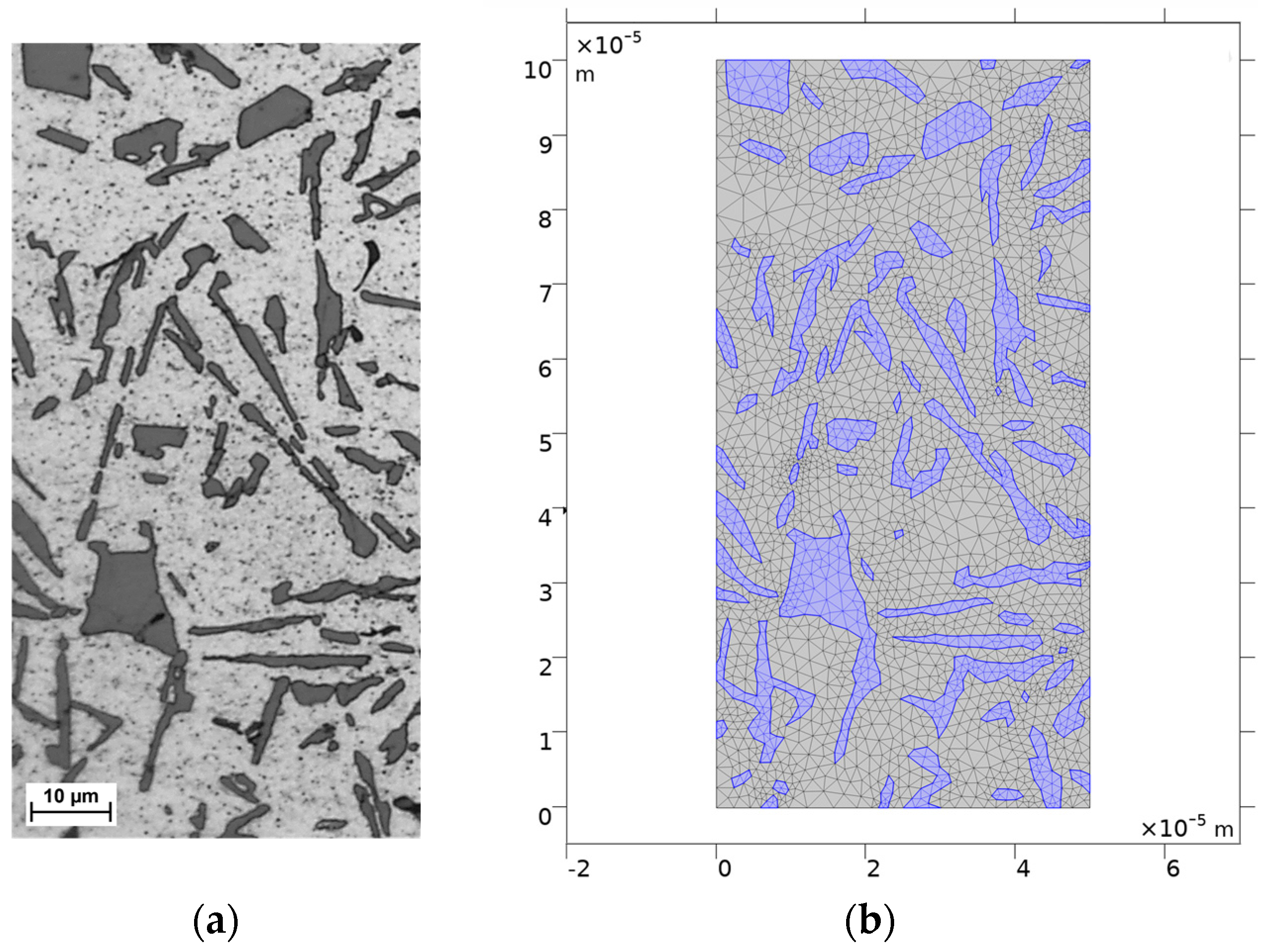
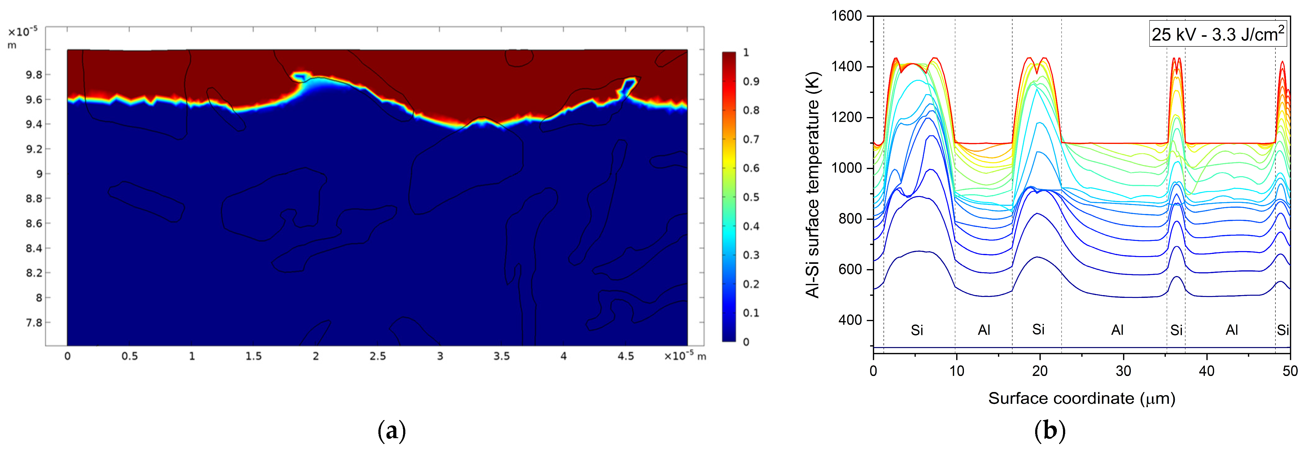
3.2. Al-Si13 Cast Alloy

The OM cross section of a hypereutectic Al-Si13 alloy produced by mould casting is shown in Figure 5a. The alloy was prepared by mirror polishing up to 1 µm diamond paste followed by a metallographic chemical attack with Keller solution. In the micrograph, a clear distinction can be appreciated between the dark grey Si, in the eutectic structure and as primary particles, and the light grey Al matrix. For the Al and Si phases, the relevant temperature-dependent properties (i.e., thermal conductivity and specific heat capacity) were taken from [20,21] and [21,22], respectively. The melting point of the system (855 K) was calculated from the Al-Si phase diagram [23], in correspondence with the precise composition measured by EDX, while the boiling points at the working pressure are from [24]. Figure 5b shows the corresponding meshed geometry created by the open-source software ImageJ (version 1.53k) from the optical micrograph. Figure 6a shows the maximum molten thickness on the Al-Si13 alloy cross section after a 25 kV electron beam pulse: the red colour indicates the liquid phase, while the blue one is the solid phase. The rainbow-coloured small layer found at the interface between solid and liquid represents the region where the transition occurs. The melting front does not proceed evenly through the material due to the presence of two different solid phases (i.e., Al and Si) with different thermal properties. In particular, silicon has a lower thermal conductivity with respect to aluminium, while their heat capacities are comparable. The maximum measurable molten thickness is about 8 µm and it is found in the correspondence of the largest portion of aluminium matrix exposed to the electron beam source, 30 µm from the left side of the cross section (Figure 6a).
Si has a higher melting point (1687 K) with respect to Al (933 K) and, in fact, the lowest molten thickness can be seen inside the coarse silicon area at 20 µm from the left side of the cross section. The difference in molten thickness should not be ascribed to electron penetration depth into Al and Si. As shown in Figure 2, where the energy density curves for different metals are reported, the peak in the energy profile is around 1.6–1.7 µm in depth for both the constituents of the alloy. During the period in which both metals are molten, liquid phase mixing occurs, and silicon particles are gradually, pulse after pulse, dissolved inside the aluminium matrix. The high cooling velocity induced by LEHCEB, discussed in Figure 4a, hinders the reprecipitation of Si particles while the material is solidifying, in an opposite manner to what happens during the casting of alloys. It was found experimentally that the surface elemental distribution changes drastically after electron beam irradiation and the chemical composition is homogenised [25]. As a consequence, the liquid phase front should propagate more evenly within the material as the number of electron beam pulses increases, contrary to what is shown for the first irradiation in Figure 6a. Figure 6b shows the surface temperature evolution during an electron beam pulse at 25 kV. In the plot, each line corresponds to a 0.1 µs timestep and the different colours helps to visually distinguish between low-temperature (blue) and high-temperature (red) instants. Si and Al areas are highlighted by vertical dashed lines. Temperature evolution within the silicon phase is radically different with respect to the aluminium one, particularly after 0.5–0.6 µs. Si quickly reaches its boiling point, remaining at that temperature for a longer time with respect to Al. It was found experimentally that Si wt.% decreases after LEHCEB treatment, confirming the modelled preferential evaporation of this component. The temperature profile inside Si particles is not symmetrical, especially at intermediate stages of the electron beam pulse. Moreover, it can be observed that small Si particles tend to heat up slower rather than large ones, where, instead, temperature builds up quickly. This behaviour can be qualitatively justified by considering the shape of each particle and the extent of the interface with the Al. Aluminium acts as a sort of sink that allows heat to dissipate from the peripheral region of the Si. As a consequence, the hottest areas of aluminium are those directly in contact with the primary or eutectic Si, where the first droplets of liquid start to form and where evaporation is more intense.

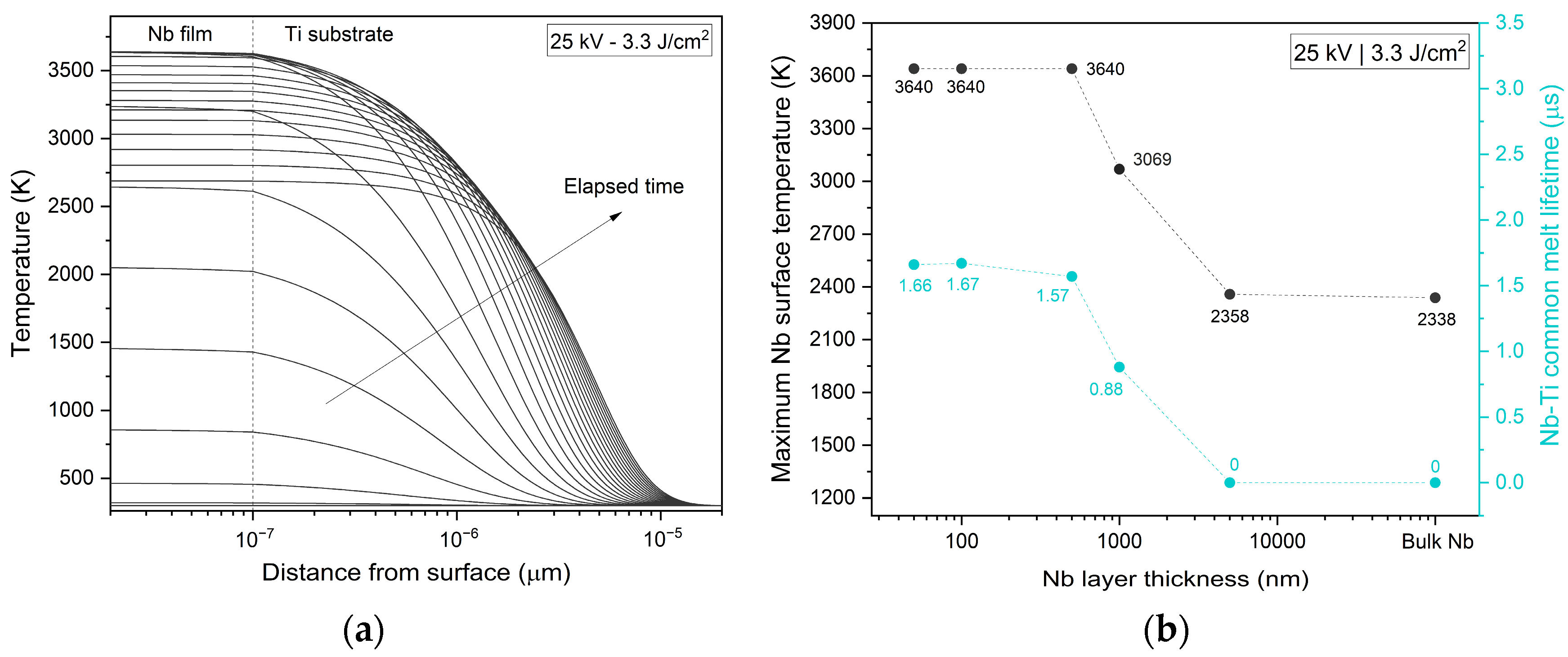
3.3. Ti-Nb Surface Alloy

LEHCEB irradiation of film–substrate systems is frequently employed to produce compositionally graded surface alloys. In such cases, the thin film is brought to the molten state together with the substrate, allowing for their liquid phase intermixing. The modelling of the Ti-Nb system follows the experimental investigation of the synthesis of the binary surface alloy [26]. The SEM fracture micrograph of a Nb thin film deposited by Magnetron Sputtering on (1 0 0) monocrystalline Si, employed to precisely calculate the MS deposition rate, is shown in Figure 7a. The deposition was performed from a Nb target, at a working pressure of 3.3 × 10⁻³ Torr, by applying a 315 V bias and varying the time to obtain different film thicknesses. Figure 7b shows the meshed geometry created to model the LEHCEB irradiation of a Nb thin film deposited on grade 1 Ti substrate. The relevant temperature-dependent properties of Ti and Nb (i.e., thermal conductivity and specific heat capacity) were taken from [21,27] and [21,28], respectively. The boiling point of niobium was qualitatively lowered to account for the working pressure within the vacuum chamber. Figure 8a shows the temperature profile along the depth of a Nb (100 nm)-Ti system for a single 25 kV electron beam pulse. Each line in the plot corresponds to a 0.1 µs time step. Close to the surface, the temperature grows until around 1.5 µs, where the peak of the beam-delivered power lies, after which it starts to drop. Instead, the temperature calculated at larger depths (i.e., below 2 µm) monotonically increases for the whole duration of the pulse, due to heat conduction taking place from the surface to the bulk. Moreover, a sharp change in the slope of the temperature line can be appreciated across the Nb-Ti interface due to their different thermal conductivity and heat capacity. The largest thermal effects occur within the first few µm of the system, while at higher depth, the temperature rapidly decreases to room temperature. This behaviour is typical of LEHCEB-irradiated systems, in which the surface modification interests only the skin of the material. Figure 8b shows a comparison between the maximum surface temperature on the Nb film surface and the Nb-Ti common melt lifetime, as a function of the film thickness. The Nb-Ti common melt lifetime is the interval in which both the metals are liquid at the interface between film and substrate. During such a period, the liquid intermixing takes place, leading to the formation of the surface alloy. The thickness of the Nb film plays a crucial role in the thermal response of the system; therefore, a computational and experimental optimisation of that parameter is mandatory. At low thickness (few nm), the surface temperature is similar to the one of the Ti substrate. In contrast, at high thickness (few µm), the surface temperature tends toward that of pure Nb. For intermediate thickness, the behaviour is given by a complex interplay between the thermal properties of the two metals. In general, the low thermal conductivity of titanium favours the build-up of temperature within the niobium layer. This phenomenon improves the probability of liquid phase formation even at moderate electron accelerating voltage, even though the Nb melting point is relatively high. As shown in Figure 8b, up to 500 nm film thickness, the surface temperature is stable at the boiling point of Nb. As the film thickness increases, the thermal response of the surface tends to align with that of the simulated bulk Nb. The common melt lifetime follows the same trend as the maximum temperature, being maximum (1.67–1.57 µs) at low film thicknesses. This finding allows us to conclude that, in order to favour as much as possible the liquid intermixing between the film and the substrate, it is preferable to perform multiple alloying steps by alternating the deposition of a 100–500 nm film followed by LEHCEB melting, as already proved experimentally in previous work [29].

4. Conclusions

In the present work, COMSOL Multiphysics was employed to numerically calculate the thermal fields induced in three different metallic systems upon Low-Energy High-Current Electron Beam irradiation. The LEHCEB oscillograms were implemented to model the fast time variation in the power profile during the pulse, while the in-depth energy density distribution was calculated from a semi-empirical formula. In the first case, the irradiation of an as-sintered 17-4 PH steel produced by metal Binder Jetting was simulated to investigate the effect of the electron accelerating voltage and number of pulses. By changing the accelerating voltage from 20 to 25 and 30 kV, the maximum surface temperature and the heating rate were increased. By changing the number of pulses from 1 to 20, a non-negligible temperature builds up in the workpiece. Moreover, an asymmetrical increase in the base temperature (i.e., in between pulses) and the maximum temperature (i.e., at the end of each pulse) was observed. In the second case, the surface treatment of a biphasic Al-Si13 alloy was investigated by building a geometry that considers the thermal behaviour of both the Si structures and the Al matrix. A 25 kV electron beam pulse was modelled, keeping track of the melting transient of the system and the surface temperature variations. It was shown that the liquid phase front does not propagate evenly through the cross section of the material but rather moves preferentially in the aluminium. The surface temperature evolution allowed us to appreciate the overheating of the silicon phase with respect to the surrounding aluminium. In the third example, the heating and cooling rates of a Nb film deposited by Magnetron Sputtering on Ti grade 1 substrate were calculated, with attention to the molten lifetime of the system as a function of the film thickness. It was shown that most of the temperature rises in the first few micrometres of the material, followed by its rapid decay at a higher depth. A sharp change in the slope of the temperature curves can be observed at the Nb-Ti interface due to their different thermal properties. Moreover, it was shown that to maximise the Nb-Ti common melt lifetime (i.e., when the liquid phase intermixing occurs), the Nb thickness should not exceed a few hundred nm.

Author Contributions

Conceptualization, A.L.H. and M.B.; Data curation, A.L.H. and V.M.; Formal analysis, A.L.H., V.M. and A.M.; Funding acquisition, M.B.; Investigation, A.L.H., V.M. and A.M.; Methodology, A.L.H. and M.B.; Project administration, M.B.; Resources, M.B.; Software, A.L.H., V.M., A.M. and L.P.; Supervision, M.B.; Validation, A.L.H., V.M. and A.M.; Visualization, A.L.H. and M.B.; Writing—original draft, A.L.H. and V.M.; Writing—review & editing, A.L.H., V.M., A.M., L.P. and M.B. All authors have read and agreed to the published version of the manuscript.

Funding

This research was funded by Fondazione Cariplo, grant n° 2020_1156.

Data Availability Statement

The data presented in this study are available on request.

Acknowledgments

Authors thank Maksim Bahdanchyk for the fruitful discussions.

Conflicts of Interest

The authors declare no conflicts of interest.

References

  1. Proskurovsky, D.I.; Rotshtein, V.P.; Ozur, G.E.; Ivanov, Y.F.; Markov, A.B. Physical foundations for surface treatment of materials with low energy, high current electron beams. Surf. Coat. Technol. 2000, 125, 49–56. [Google Scholar] [CrossRef]
  2. Rotshtein, V.P.; Proskurovsky, D.I.; Ivanov, Y.F.; Markov, A.B. Surface modification and alloying of metallic materials with low-energy high-current electron beams. Surf. Coat. Technol. 2004, 180, 377–381. [Google Scholar] [CrossRef]
  3. Proskurovsky, D.I.; Rotshtein, V.P.; Ozur, G.E. Use of low-energy, high-current electron beams for surface treatment of materials. Surf. Coat. Technol. 1997, 96, 117–122. [Google Scholar] [CrossRef]
  4. Vladimir, R.; Ivanov, Y.; Markov, A. Surface treatment of materials with low-energy, high-current electron beams. Mater. Surf. Process. By Dir. Energy Tech. 2006, 6, 205. [Google Scholar]
  5. Markov, A.B.; Solovyov, A.V. Melting Thresholds of the Film-Substrate System Irradiated with a Low-Energy High-Current Electron Beam. Russ. Phys. J. 2023, 65, 1893–1899. [Google Scholar] [CrossRef]
  6. Markov, A.; Yakovlev, E. Calculation of heat regimes for a Cr-Cu surface alloy formed with a low-energy high-current electron beam. J. Phys. Conf. Ser. 2018, 1115, 042010. [Google Scholar] [CrossRef]
  7. Markov, A.; Yakovlev, E. Calculation of heat regimes for a Ni-Al surface alloy formed on a carbon steel substrate with a low-energy high-current electron beam. J. Phys. Conf. Ser. 2019, 1393, 012130. [Google Scholar]
  8. Markov, A.; Solovyov, A.; Yakovlev, E.; Pesterev, E.; Petrov, V.; Slobodyan, M. Computer simulation of temperature fields in the Cr (film)-Zr (substrate) system during pulsed electron-beam irradiation. J. Phys. Conf. Ser. 2021, 2064, 012058. [Google Scholar] [CrossRef]
  9. Markov, A.; Solovyov, A.; Yakovlev, E.; Slobodyan, M. Prediction of the composition of surface alloys formed via pulsed melting of preliminary deposited coatings. Mater. Chem. Phys. 2022, 292, 126821. [Google Scholar] [CrossRef]
  10. Shepel, D.; Markov, A. Low-energy high-current electron beam heating of target with second-phase microinclusions. Tech. Phys. Lett. 2011, 37, 772–775. [Google Scholar] [CrossRef]
  11. Vutova, K.; Donchev, V. Electron beam melting and refining of metals: Computational modeling and optimization. Materials 2013, 6, 4626–4640. [Google Scholar] [CrossRef] [PubMed]
  12. Yan, W.; Smith, J.; Ge, W.; Lin, F.; Liu, W.K. Multiscale modeling of electron beam and substrate interaction: A new heat source model. Comput. Mech. 2015, 56, 265–276. [Google Scholar] [CrossRef]
  13. Kurashkin, S.; Rogova, D.; Tynchenko, V.; Petrenko, V.; Milov, A. Modeling of Product Heating at the Stage of Beam Input in the Process of Electron Beam Welding Using the COMSOL Multiphysics System. In Proceedings of the Computational Methods in Systems and Software, Virtual, 14–17 October 2020; Springer International Publishing: Cham, Switzerland, 2020; pp. 905–912. [Google Scholar]
  14. Ansari, P.; Rehman, A.U.; Pitir, F.; Veziroglu, S.; Mishra, Y.K.; Aktas, O.C.; Salamci, M.U. Selective laser melting of 316l austenitic stainless steel: Detailed process understanding using multiphysics simulation and experimentation. Metals 2021, 11, 1076. [Google Scholar] [CrossRef]
  15. Mayi, Y.A.; Dal, M.; Peyre, P.; Metton, C.; Moriconi, C.; Fabbro, R. An original way of using COMSOL® application builder to enhance multiphysical simulation of laser welding processes. In Proceedings of the COMSOL Conference 2020, Virtual, 7–8 October 2020; pp. 14–15. [Google Scholar]
  16. Mayi, Y.A.; Dal, M.; Peyre, P.; Bellet, M.; Metton, C.; Moriconi, C.; Fabbro, R. Laser-induced plume investigated by finite element modelling and scaling of particle entrainment in laser powder bed fusion. J. Phys. D Appl. Phys. 2019, 53, 075306. [Google Scholar] [CrossRef]
  17. Darif, M.; Semmar, N.; Orléans Cedex, F. Numerical simulation of Si nanosecond laser annealing by COMSOL multiphysics. In Proceedings of the COMSOL Conference 2008, Hannover, Germany, 9–11 October 2008; pp. 567–571. [Google Scholar]
  18. Sabau, A.S.; Porter, W.D. Alloy shrinkage factors for the investment casting of 17-4PH stainless steel parts. Metall. Mater. Trans. B Process Metall. Mater. Process. Sci. 2008, 39, 317–330. [Google Scholar] [CrossRef]
  19. Fabiocchi, L.; Mariani, M.; Lucchini Huspek, A.; Pozzi, M.; Bestetti, M.; Lecis, N. Low-Energy High-Current Pulsed Electron Beam Surface Treatment on the Tribological Behavior of 17-4PH Steel Produced via Binder Jetting. Lubricants 2025, 13, 42. [Google Scholar] [CrossRef]
  20. Brandt, R.; Neuer, G. Electrical resistivity and thermal conductivity of pure aluminum and aluminum alloys up to and above the melting temperature. Int. J. Thermophys. 2007, 28, 1429–1446. [Google Scholar] [CrossRef]
  21. NIST Chemistry—National Institute of Standards and Technology. Available online: https://webbook.nist.gov/ (accessed on 20 February 2025).
  22. Yamasue, E.; Susa, M.; Fukuyama, H.; Nagata, K. Thermal conductivities of silicon and germanium in solid and liquid states measured by non-stationary hot wire method with silica coated probe. J. Cryst. Growth 2002, 234, 121–131. [Google Scholar] [CrossRef]
  23. Asensio-Lozano, J.; Vander Voort, G. The Al-Si Phase Diagram. Tech Notes 2009, 5, 5. [Google Scholar]
  24. Antes, H., Jr. Critical Melting Points and Reference Data for Vacuum Heat Treating. 2010. Available online: https://solarmfg.com/wp-content/uploads/2011/01/Critical-Melting-Point1.pdf (accessed on 20 February 2025).
  25. Lucchini Huspek, A.; Akdogan, B.; Akhmadeev, Y.H.; Petrikova, E.A.; Ivanov, Y.F.; Moskvin, P.V.; Koval, N.N.; Bestetti, M. Enhancing Microhardness and Corrosion Resistance of Anodic Oxides Grown on Hypoeutectic Al–Si Alloys Pretreated by Low-Energy High-Current Electron Beams. J. Surf. Investig. X-Ray Synchrotron Neutron Tech. 2024, 18, 1135–1145. [Google Scholar] [CrossRef]
  26. Morini, F.; Bestetti, M.; Franz, S.; Vicenzo, A.; Markov, A.; Yakovlev, E. Synthesis and characterization of ti-nb alloy films obtained by magnetron sputtering and low-energy high-current electron beam treatment. Materials 2021, 14, 3238. [Google Scholar] [CrossRef] [PubMed]
  27. Mills, K.C. Recommended Values of Thermophysical Properties for Selected Commercial Alloys; Woodhead Publishing: Cambridge, UK, 2002. [Google Scholar]
  28. Singaravelu, S.; Klopf, J.M.; Krafft, G.; Kelley, M.J. Laser nitriding of niobium for application to superconducting radio-frequency accelerator cavities. J. Vac. Sci. Technol. B 2011, 29, 061803. [Google Scholar] [CrossRef]
  29. Markov, A.; Yakovlev, E.; Bestetti, M. Synthesis of a Cr-Cu surface alloy using a low-energy high-current electron beam. Results Phys. 2019, 12, 1915–1924. [Google Scholar] [CrossRef]
Figure 1. Electron beam power density curves recorded at different accelerating voltages: (a) 20 kV, (b) 25 kV, and (c) 30 kV.
Jmmp 09 00130 g001
Figure 2. Energy density curves calculated from Equations (17) and (18) for different metals at 25 kV electron accelerating voltage.
Jmmp 09 00130 g002
Figure 3. SEM cross section image of as-sintered 17-4 PH steel produced by metal Binder Jetting (a) and corresponding meshed geometry used in COMSOL Multiphysics (b) where the boundary exposed to the LEHCEB surface treatment is highlighted in blue.
Jmmp 09 00130 g003
Figure 4. Surface temperature during single pulse at different electron accelerating voltage (a) and evolution of minimum and maximum temperature at 25 kV and 20 pulses (b).
Jmmp 09 00130 g004
Figure 5. Optical microscope cross section of mould casting hypereutectic Al-Si13 alloy (a) and corresponding meshed geometry used in COMSOL Multiphysics (b) where silicon areas are highlighted in purple.
Jmmp 09 00130 g005
Figure 6. Calculated liquid front on the cross section after a 25 kV electron beam pulse (a) and the evolution of the surface temperature during a 25 kV electron beam pulse (Al and Si highlighted) (b).
Jmmp 09 00130 g006
Figure 7. SEM cross section of Nb thin film deposited by DC Magnetron Sputtering on monocrystalline Si (a) and Nb-Ti meshed geometry used in COMSOL Multiphysics (b) where the niobium layer is highlighted in purple.
Jmmp 09 00130 g007
Figure 8. Depth temperature profile during single electron beam pulse: each line corresponds to 0.1 µs timestep (a) and comparison between Nb surface temperature and Nb-Ti common melt lifetime (b).
Jmmp 09 00130 g008
Table 1. Parameters used in COMSOL Multiphysics models.
ParameterValueDescription
Ep2.5, 3.3, 4.9 J/cm2Energy density at 20, 25, 30 kV
τp2.5 µsAverage pulse duration
Np1-…Number of pulses
ωp0.05–0.1 HzPulse repetition frequency
Pirr1.8 × 10−4 TorrIrradiation pressure
Tamb273.15 KAmbient temperature
RH0.35Ambient relative humidity
Disclaimer/Publisher’s Note: The statements, opinions and data contained in all publications are solely those of the individual author(s) and contributor(s) and not of MDPI and/or the editor(s). MDPI and/or the editor(s) disclaim responsibility for any injury to people or property resulting from any ideas, methods, instructions or products referred to in the content.

