
Ab Initio Modelling of g-ZnO Deposition on the Si (111) Surface


Abstract
:1. Introduction
2. Models and Methods
3. Results and Discussion
4. Conclusions
Author Contributions
Funding
Data Availability Statement
Acknowledgments
Conflicts of Interest
References
- Mohamed, K.M.; Benitto, J.J.; Vijaya, J.J.; Bououdina, M. Recent Advances in ZnO-Based Nanostructures for the Photocatalytic Degradation of Hazardous, Non-Biodegradable Medicines. Crystals 2023, 13, 329. [Google Scholar] [CrossRef]
- Sheikhi, S.; Aliannezhadi, M.; Tehrani, F.S. The Effect of PEGylation on Optical and Structural Properties of ZnO Nanostructures for Photocatalyst and Photodynamic Applications. Mater. Today Commun. 2023, 34, 105103. [Google Scholar] [CrossRef]
- Alnaim, N.; Kumar, S.; Alshoaibi, A. Structural, Morphological, Electronic Structural, Optical, and Magnetic Properties of ZnO Nanostructures. Materials 2022, 15, 8889. [Google Scholar] [CrossRef] [PubMed]
- Morandi, S.; Fioravanti, A.; Cerrato, G.; Lettieri, S.; Sacerdoti, M.; Carotta, M.C. Facile Synthesis of ZnO Nano-Structures: Morphology Influence on Electronic Properties. Sens. Actuators B Chem. 2017, 249, 581–589. [Google Scholar] [CrossRef]
- Ayoub, I.; Kumar, V.; Abolhassani, R.; Sehgal, R.; Sharma, V.; Sehgal, R.; Swart, H.C.; Mishra, Y.K. Advances in ZnO: Manipulation of Defects for Enhancing Their Technological Potentials. Nanotechnol. Rev. 2022, 11, 575–619. [Google Scholar] [CrossRef]
- Bhandari, K.P.; Sapkota, D.R.; Jamarkattel, M.K.; Stillion, Q.; Collins, R.W. Zinc Oxide Nanoparticles—Solution-Based Synthesis and Characterizations. Nanomaterials 2023, 13, 1795. [Google Scholar] [CrossRef] [PubMed]
- Ortiz-Casas, B.; Galdámez-Martínez, A.; Gutiérrez-Flores, J.; Baca Ibañez, A.; Kumar Panda, P.; Santana, G.; de la Vega, H.A.; Suar, M.; Gutiérrez Rodelo, C.; Kaushik, A.; et al. Bio-Acceptable 0D and 1D ZnO Nanostructures for Cancer Diagnostics and Treatment. Mater. Today 2021, 50, 533–569. [Google Scholar] [CrossRef]
- Trivedi, S.; Nemade, H.B. ZnO Nanorod-based Love Wave Delay Line for High Mass Sensitivity: A Finite Element Analysis. IET Sci. Meas. Technol. 2019, 13, 1245–1253. [Google Scholar] [CrossRef]
- Ebert, M.; Ghazali, N.A.B.; Kiang, K.S.; Zeimpekis, I.; Maerz, B.; de Planque, M.R.R.; Chong, H.M.H. Multichannel ZnO Nanowire Field Effect Transistors by Lift-off Process. Nanotechnology 2018, 29, 415302. [Google Scholar] [CrossRef] [PubMed]
- Bardakas, A.; Kaidatzis, A.; Tsamis, C. A Review of Magnetoelectric Composites Based on ZnO Nanostructures. Appl. Sci. 2023, 13, 8378. [Google Scholar] [CrossRef]
- Schlur, L.; Calado, J.R.; Spitzer, D. Synthesis of Zinc Oxide Nanorods or Nanotubes on One Side of a Microcantilever. R. Soc. Open Sci. 2018, 5, 180510. [Google Scholar] [CrossRef] [PubMed]
- Del Gobbo, S.; Poolwong, J.; D’Elia, V.; Ogawa, M. Simultaneous Controlled Seeded-Growth and Doping of ZnO Nanorods with Aluminum and Cerium: Feasibility Assessment and Effect on Photocatalytic Activity. Cryst. Growth Des. 2020, 20, 5508–5525. [Google Scholar] [CrossRef]
- Rezaie, M.N.; Mohammadnejad, S.; Ahadzadeh, S. The Impact of ZnO Nanotube on the Performance of Hybrid Inorganic/Organic Light-Emitting Diode as a Single-Mode Ring-Core UV Waveguide. Surf. Interfaces 2022, 28, 101666. [Google Scholar] [CrossRef]
- Real, S.; Espíndola, O.; Zelaya, M.P.; Marin, O.; Comedi, D.; Tirado, M. Single-Step Zno Nanorod Bunches Formation on p-Type Si-Conductive Substrates by Electrophoretic Deposition. Surf. Interfaces 2021, 23, 100930. [Google Scholar] [CrossRef]
- Alshgari, R.A.; Ujjan, Z.A.; Shah, A.A.; Bhatti, M.A.; Tahira, A.; Shaikh, N.M.; Kumar, S.; Ibupoto, M.H.; Elhawary, A.; Nafady, A.; et al. ZnO Nanostructures Doped with Various Chloride Ion Concentrations for Efficient Photocatalytic Degradation of Methylene Blue in Alkaline and Acidic Media. Molecules 2022, 27, 8726. [Google Scholar] [CrossRef] [PubMed]
- Lahmer, M.A. Effect of Doping with Sulfur Atoms on the Electronic and Photocatalytic Properties of the ZnO(100) Surface: A DFT+U Study. Comput. Condens. Matter 2022, 31, e00654. [Google Scholar] [CrossRef]
- Vaddadi, V.S.C.S.; Parne, S.R.; Pothukanuri, N.; Sriram, S.R.; Yelsani, V. Investigattions on ZnO Thin Films Modified with Urea: An Approach as Ammonia Sensor. ACS Omega 2023, 8, 17719–17730. [Google Scholar] [CrossRef] [PubMed]
- Zeljković, S.; Balaban, M.; Gajić, D.; Vračević, S.; Ivas, T.; Vranković, D.; Jelić, D. Mechanochemically Induced Synthesis of N-Ion Doped ZnO: Solar Photocatalytic Degradation of Methylene Blue. Green Chem. Lett. Rev. 2022, 15, 869–880. [Google Scholar] [CrossRef]
- Stoltz, K.R.; Echeverria, E.; Kaphle, A.; Austin, A.J.; Harikumar, P.; Yost, A.J.; McIlroy, D.N.; Borunda, M.F. Optimization of the U Parameter in CoO Groupings in ZnO(100). Comput. Mater. Sci. 2021, 198, 110700. [Google Scholar] [CrossRef]
- Garratt, E.; Prete, P.; Lovergine, N.; Nikoobakht, B. Observation and Impact of a “Surface Skin Effect” on Lateral Growth of Nanocrystals. J. Phys. Chem. C 2017, 121, 14845–14853. [Google Scholar] [CrossRef]
- Ahmad, S.; Usman, M.; Hashim, M.; Ali, A.; Shah, R.; Rahman, N.U. Investigation of Optical and Dielectric Properties of Nickel-Doped Zinc Oxide Nanostructures Prepared via Coprecipitation Method. Nanomater. Nanotechnol. 2024, 2024, 8330886. [Google Scholar] [CrossRef]
- McPeak, K.M.; Baxter, J.B. ZnO Nanowires Grown by Chemical Bath Deposition in a Continuous Flow Microreactor. Cryst. Growth Des. 2009, 9, 4538–4545. [Google Scholar] [CrossRef]
- Wang, L.-H.; Fu, S.-L.; Wang, C.-A.; Gan, G.-R.; Xie, Y.-P.; Gao, X.-L. The Electromagnetic Properties of ZnO Quantum Dot with Different Mn-Doping Sites. J. Supercond. Nov. Magn. 2023, 36, 637–646. [Google Scholar] [CrossRef]
- Luo, J.T.; Zhu, X.Y.; Chen, G.; Zeng, F.; Pan, F. The Electrical, Optical and Magnetic Properties of Si-Doped ZnO Films. Appl. Surf. Sci. 2012, 258, 2177–2181. [Google Scholar] [CrossRef]
- Said, K.; Baghdad, R. Carbon and Silicon Co-Doping Effect on Microstructural and Optoelectronic Properties of ZnO: An Ab Initio Study. Optik 2022, 260, 169138. [Google Scholar] [CrossRef]
- Mohammadigharehbagh, R.; Özen, S.; Yudar, H.H.; Pat, S.; Korkmaz, Ş. The Electrical, Elemental, Optical, and Surface Properties of Si-Doped ZnO Thin Films Prepared by Thermionic Vacuum Arc. Mater. Res. Express 2017, 4, 096404. [Google Scholar] [CrossRef]
- Zhang, H.; Lu, S.; Xu, W.; Yuan, F. First-Principles Study of Si Atoms Adsorbed on ZnO (0001) Surface and the Effect on Electronic and Optical Properties. Surf. Sci. 2014, 625, 30–36. [Google Scholar] [CrossRef]
- Xu, H.-Y.; Zhang, S.-Q.; Wang, Y.-F.; Xu, Y.; Dong, L.-M.; Komarneni, S. New Insights into the Photocatalytic Mechanism of Pristine ZnO Nanocrystals: From Experiments to DFT Calculations. Appl. Surf. Sci. 2023, 614, 156225. [Google Scholar] [CrossRef]
- Rojas-Chávez, H.; Miralrio, A.; Hernández-Rodríguez, Y.M.; Cruz-Martínez, H.; Pérez-Pérez, R.; Cigarroa-Mayorga, O.E. Needle- and Cross-Linked ZnO Microstructures and Their Photocatalytic Activity Using Experimental and DFT Approach. Mater. Lett. 2021, 291, 129474. [Google Scholar] [CrossRef]
- van Mourik, T.; Bühl, M.; Gaigeot, M.-P. Density Functional Theory across Chemistry, Physics and Biology. Philos. Trans. R. Soc. A Math. Phys. Eng. Sci. 2014, 372, 20120488. [Google Scholar] [CrossRef] [PubMed]
- Sibanda, D.; Oyinbo, S.T.; Jen, T.-C. A Review of Atomic Layer Deposition Modelling and Simulation Methodologies: Density Functional Theory and Molecular Dynamics. Nanotechnol. Rev. 2022, 11, 1332–1363. [Google Scholar] [CrossRef]
- Brahim, N.; Thotagamuge, R.; Kooh, M.; Lim, C.; Syaahiran, M.; Usman, A.; Shahri, N.; Chou Chau, Y.-F.; Chou Chao, C.-T.; Chiang, H.-P.; et al. Enhanced CO Gas Sensing with DFT Optimized PbS Loading on ZnO and CrZnO Nanocomposites. Sustainability 2022, 14, 13978. [Google Scholar] [CrossRef]
- Claeyssens, F.; Freeman, C.L.; Allan, N.L.; Sun, Y.; Ashfold, M.N.R.; Harding, J.H. Growth of ZnO Thin Films—Experiment and Theory. J. Mater. Chem. 2005, 15, 139–148. [Google Scholar] [CrossRef]
- Kresse, G.; Furthmüller, J. Efficient Iterative Schemes for Ab Initio Total-Energy Calculations Using a Plane-Wave Basis Set. Phys. Rev. B 1996, 54, 11169–11186. [Google Scholar] [CrossRef] [PubMed]
- Blöchl, P.E. Projector Augmented-Wave Method. Phys. Rev. B 1994, 50, 17953–17979. [Google Scholar] [CrossRef] [PubMed]
- Perdew, J.P.; Burke, K.; Ernzerhof, M. Generalized Gradient Approximation Made Simple. Phys. Rev. Lett. 1996, 77, 3865–3868. [Google Scholar] [CrossRef] [PubMed]
- Liechtenstein, A.I.; Anisimov, V.I.; Zaanen, J. Density-Functional Theory and Strong Interactions: Orbital Ordering in Mott-Hubbard Insulators. Phys. Rev. B 1995, 52, R5467–R5470. [Google Scholar] [CrossRef]
- Ramanarayanan, P.; Sabirianov, R.F.; Cho, K. Point Defect Energetics in Silicon Using the LDA+ U Method. arXiv 2003, arXiv:cond-mat/0310606. [Google Scholar]
- Lee, Y.-S.; Peng, Y.-C.; Lu, J.-H.; Zhu, Y.-R.; Wu, H.-C. Electronic and Optical Properties of Ga-Doped ZnO. Thin Solid Films 2014, 570, 464–470. [Google Scholar] [CrossRef]
- Ma, X.; Wu, Y.; Lv, Y.; Zhu, Y. Correlation Effects on Lattice Relaxation and Electronic Structure of ZnO within the GGA+U Formalism. J. Phys. Chem. C 2013, 117, 26029–26039. [Google Scholar] [CrossRef]
- Monkhorst, H.J.; Pack, J.D. Special Points for Brillouin-Zone Integrations. Phys. Rev. B 1976, 13, 5188–5192. [Google Scholar] [CrossRef]
- Ren, J.; Zhang, H.; Cheng, X. Electronic and Magnetic Properties of All 3d Transition-Metal-Doped ZnO Monolayers. Int. J. Quantum Chem. 2013, 113, 2243–2250. [Google Scholar] [CrossRef]
- Tau, O.; Lovergine, N.; Prete, P. Adsorption and Decomposition Steps on Cu(111) of Liquid Aromatic Hydrocarbon Precursors for Low-Temperature CVD of Graphene: A DFT Study. Carbon 2023, 206, 142–149. [Google Scholar] [CrossRef]
- Lu, G.-H.; Huang, M.; Cuma, M.; Liu, F. Relative Stability of Si Surfaces: A First-Principles Study. Surf. Sci. 2005, 588, 61–70. [Google Scholar] [CrossRef]


| Potentials | Hubbard Correction | |||||
|---|---|---|---|---|---|---|
| Element | Free Electrons | Potential Cut-Off Energy, eV | Orbital | U, eV | J, eV | Source |
| Si | 3s23p2 | 245.345 | p | 0 | 4 | [38] |
| Zn | 3d104p2 | 276.723 | d | 10 | 0 | [39,40] |
| O | 2s22p4 | 400 | p | 7 | 0 | [39,40] |
| Si/g-ZnO | ZnO | 1 | 2 | 3 | |||
|---|---|---|---|---|---|---|---|
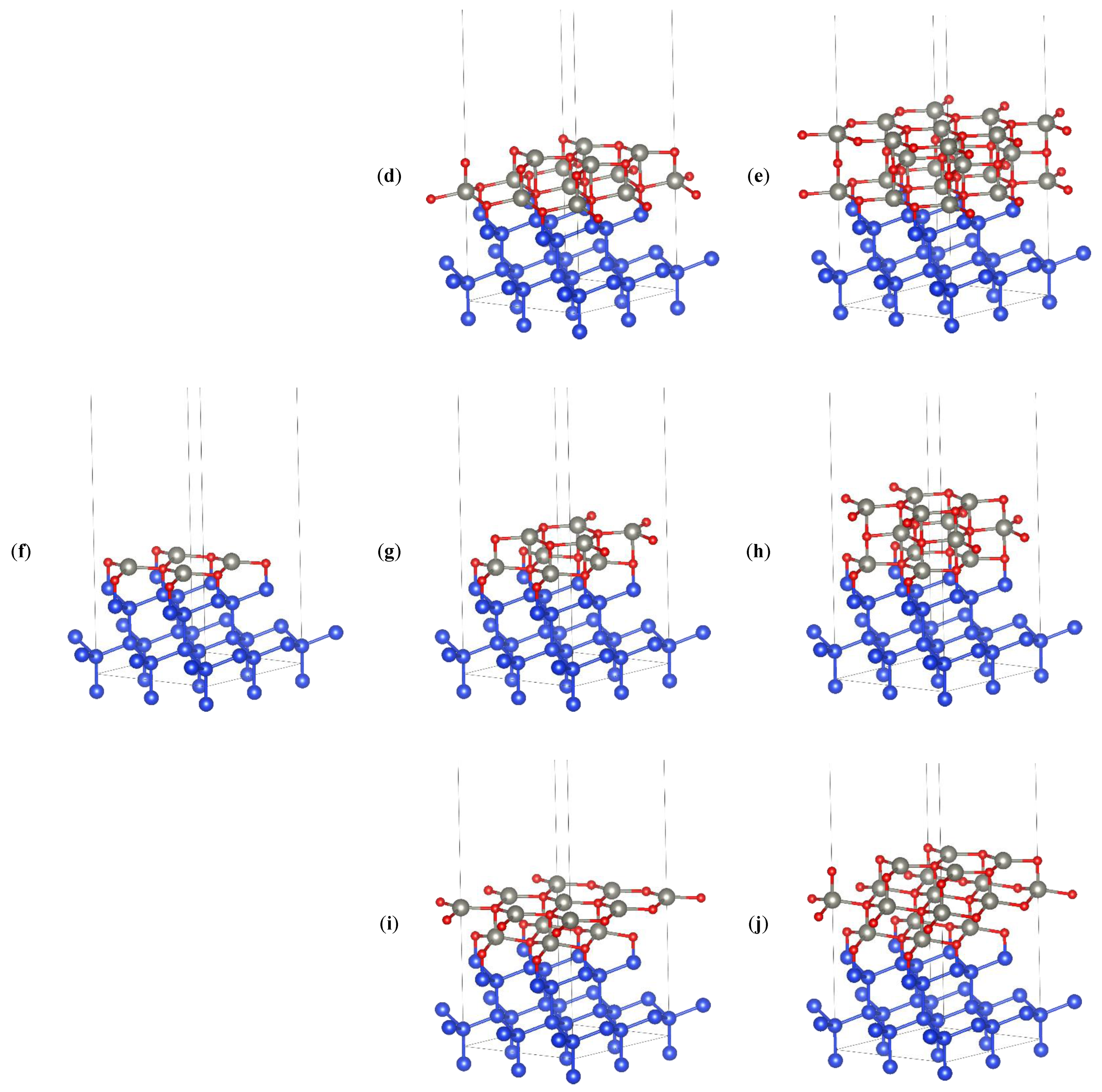
| sphalerite | sphalerite | 0.12 | Figure 4a | 0.56 | Figure 4b | 0.53 | Figure 4c |
| sphalerite | wurtzite | 0.49 | Figure 4d | −0.07 | Figure 4e | ||
| wurtzite | wurtzite | 0.04 | Figure 4f | 0.44 | Figure 4g | −0.06 | Figure 4h |
| wurtzite | sphalerite | 0.57 | Figure 4i | 0.52 | Figure 4j |
| Number of ZnO Layers | ||||
|---|---|---|---|---|
| Si/ZnO Interface | ZnO Stacking | 1 | 2 | 3 |
| sphalerite | wurtzite | vacuum | ||
| 0.29 | 0.16 | 0.15 | ||
| 1.71 | 1.86 | 1.89 | ||
| Si | 0.62 | 0.49 | ||
| 1.69 | 1.81 | |||
| Si | 0.61 | |||
| 1.69 | ||||
| Si | ||||
| sphalerite | vacuum | |||
| 0.07 | 0.04 | |||
| 1.86 | 1.91 | |||
| 0.38 | 0.10 | |||
| 1.72 | 1.85 | |||
| Si | 0.05 | |||
| 1.73 | ||||
| Si | ||||
| wurtzite | wurtzite | vacuum | ||
| 0.24 | 0.04 | 0.03 | ||
| 1.71 | 1.85 | 1.85 | ||
| Si | 0.24 | 0.11 | ||
| 1.71 | 1.83 | |||
| Si | 0.10 | |||
| 1.73 | ||||
| Si | ||||
| sphalerite | vacuum | |||
| 0.17 | 0.12 | |||
| 1.86 | 1.88 | |||
| 0.49 | 0.46 | |||
| 1.68 | 1.81 | |||
| Si | 0.49 | |||
| 1.68 | ||||
| Si | ||||
| Si/ZnO Sphalerite | Number of ZnO Layers | ZnO Stacking | |
|---|---|---|---|
| Wurtzite | Sphalerite | ||
| sphalerite | 1 | 0.12 | |
| 2 | 0.61 | ||
| 3 | 0.54 | ||
| 2 | 0.68 | ||
| 3 | 1.21 | ||
| wurtzite | 1 | 0.04 | |
| 2 | 0.48 | ||
| 3 | 0.42 | ||
| 2 | 0.62 | ||
| 3 | 1.14 | ||
Disclaimer/Publisher’s Note: The statements, opinions and data contained in all publications are solely those of the individual author(s) and contributor(s) and not of MDPI and/or the editor(s). MDPI and/or the editor(s) disclaim responsibility for any injury to people or property resulting from any ideas, methods, instructions or products referred to in the content. |
© 2024 by the authors. Licensee MDPI, Basel, Switzerland. This article is an open access article distributed under the terms and conditions of the Creative Commons Attribution (CC BY) license (https://creativecommons.org/licenses/by/4.0/).
Share and Cite
Alzhanova, A.; Mastrikov, Y.; Yerezhep, D. Ab Initio Modelling of g-ZnO Deposition on the Si (111) Surface. J. Compos. Sci. 2024, 8, 281. https://doi.org/10.3390/jcs8070281
Alzhanova A, Mastrikov Y, Yerezhep D. Ab Initio Modelling of g-ZnO Deposition on the Si (111) Surface. Journal of Composites Science. 2024; 8(7):281. https://doi.org/10.3390/jcs8070281
Chicago/Turabian StyleAlzhanova, Aliya, Yuri Mastrikov, and Darkhan Yerezhep. 2024. "Ab Initio Modelling of g-ZnO Deposition on the Si (111) Surface" Journal of Composites Science 8, no. 7: 281. https://doi.org/10.3390/jcs8070281
APA StyleAlzhanova, A., Mastrikov, Y., & Yerezhep, D. (2024). Ab Initio Modelling of g-ZnO Deposition on the Si (111) Surface. Journal of Composites Science, 8(7), 281. https://doi.org/10.3390/jcs8070281