Abstract
An approach to derive the below-bandgap absorption in GaSb/GaAs self-assembled quantum dot devices using room-temperature external quantum efficiency measurement results is presented. Devices with five layers of delta-doped quantum dots placed in the intrinsic, n- and p-regions of a GaAs solar cell are studied. The importance of incorporating an extended Urbach tail absorption in analyzing the absorption strength of quantum dots and the transition states is demonstrated. The theoretically integrated absorbance via quantum dot ground states is calculated as 1.04 × 1015 cm−1s−1, which is in reasonable agreement with the experimentally derived value 8.1 × 1015 cm−1s−1. The wetting layer and quantum dot absorption contributions are separated from the tail absorption and their transition energies are calculated. Using these transition energies and the GaAs energy gap of 1.42 eV, the heavy hole confinement energies for the quantum dots (320 meV) and for the wetting layer (120 meV) are estimated.
1. Introduction
There is increasing interest in the incorporation of quantum dots (QDs) within the active region of GaAs-based single junction solar cells as a means of absorbing long-wavelength photons to extend the photoresponse and increase the quantum efficiency. Also, the incorporation of Type II GaSb quantum dots or quantum rings (QRs) in GaAs has been proposed as a promising system to realize an intermediate band solar cell (IBSC) [1,2]. Yasushi Shoji et al. suggest that a two-step absorption process is more dominant for carrier extraction from GaSb/GaAs QR structure [3]. These structures can also be incorporated into multijunction cells to increase the current or efficiency. However, the device design and growth must be considered to reduce defect formation due to strain accumulation. This could be achieved by the use of GaSb QRs instead of QDs, which reduces the net strain associated with the large lattice mismatch (7.8%), enabling multiple layers to be grown without generating threading dislocations or relaxed QDs [4].
Previously, we reported that Type II GaSb/GaAs quantum dots (QDs) can significantly extend the spectral response beyond the visible out towards 1.4 μm, giving a near optimum bandgap for concentrator solar cells [4]. These were grown by molecular beam epitaxy (MBE) using a Sb flux for 30 s, exploiting an efficient As–Sb exchange reaction to form a thin about 0.5 monolayer (ML) GaSb layer. The Ga and the Sb cells were then opened simultaneously and 2.1 ML of GaSb is deposited. The Sb and As fluxes were approximately 5 × 10⁻⁷ and 5 × 10⁻⁶, respectively. The Ga growth rate was approximately 0.3 ML/s.
Reflection high-energy electron diffraction (RHEED) was used to monitor surface reconstruction and was observed spotty after depositing 1.5 ML of GaSb. The solar cells were fabricated from the epitaxial material as mesa-etched diodes with a diameter of 2.5 mm using standard photolithography and wet applications [5]. This is expected to achieve below-bandgap photon absorption. The extended tail energy states (also known as Urbach tail) lead to an effective reduction in the bandgap, to an increase in the photo-generated current, and to a reduction in the open-circuit voltage [6]. Experiments have shown that QDs embedded in the depletion region could generate additional photocurrent. However, electron–hole recombination in QDs results in additional dark current, which reduces the open-circuit voltage and keeps the conversion efficiency of QD solar cells below the Shockley–Queisser limit. For the realization of IBSC, doping has been considered a desirable method to half-fill quantum dots, which facilitates a sequential two-photon absorption process from valence band to confined states and from confined states to the conduction band. The approach of placing QDs in the n-doped region or p-doped region of the solar cell and the effects of delta doping of quantum dots has been previously investigated by us [7]. We observed that devices with p- or n-doped QDs placed in the flat band potential (p- or n-doped region) showed a recovery in short-circuit current and open-circuit voltage compared to devices with delta-doped QDs placed in the depletion region. However, there was less photocurrent arising from the absorption of sub-bandgap photons. Furthermore, the long-wavelength photoresponse of the n-doped QDs placed in the n-doped region showed a slight improvement compared to the control cell. Hence, we proposed the approach of placing QDs in the n-doped region of the solar cell instead of the depletion region as a possible route towards increasing the conversion efficiency of QD solar cells. Consequently, it is also important to investigate the role of electron doping in QD devices in below-bandgap photon absorption via transitions to quantum confined states.
The purpose of this study is to investigate the effect of below-bandgap absorption of an extended Urbach tail in a QD device using room-temperature external quantum efficiency measurements. The transition energies of carriers in QDs and in a wetting layer (WL) can be determined by an analysis of below-bandgap absorption [6]. For the first time, in Ref. [6], a measurement of the external quantum efficiency (EQE)at room temperature was used to derive the spectral dependence of the QD absorption in Type I InAs/GaAs QD solar cell. The absorption coefficient of quantum dots below the bandgap depends exponentially on the photon energy given by the Urbach tail [6]. The Urbach energy characterizes the degree of disorder within the semiconductor material. For QD devices, the Urbach energy broadens because of the disruption to the lattice by built-up strain [6]. This continuum tailing density of states provides a competing path for the carriers on the intermediate states to be directly collected. In this paper, the Urbach tail absorption through EQE contribution from QDs and WL was studied for Type II GaSb/GaAs solar cell structures to address its feasibility for the realization of IBSC.
2. Materials and Methods
The GaSb QD solar cell structures were grown by MBE on GaAs substrates as shown in Figure 1. The structures contain five layers of undoped QDs (sample A) and delta-doped QDs (samples B and C) embedded in the intrinsic region, n-doped (sample D) and p-doped (sample E) regions of the GaAs p-i-n junction, where the QDs in D and E samples are spatially separated from the depletion region [7]. The QDs were grown using the Stranski–Krastanow self-assembled growth method following our previous study [5]. For samples A to D, a 1 μm thick n-type GaAs:Te base layer with a doping density of 1017 cm−3 was grown, followed by a 500 nm intrinsic region. Then, a 0.5 μm p-type GaAs:Be (2 × 1018 cm−3) emitter layer was grown. For sample E, a 1 μm thick p-type GaAs:Be base layer with a doping density of 1017 cm−3 was grown, followed by a 500 nm intrinsic region. Then, a 0.5 μm n-type GaAs:Te (2 × 1017 cm−3) emitter layer was grown. Finally, a 50 nm Al0.8Ga0.2As window layer and a thin 50 nm GaAs cap were grown.
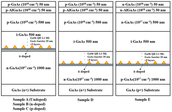
Figure 1.
Schematic structure of quantum dot solar cells (QDSCs): sample A—undoped QDs grown in intrinsic region, sample B—n-doped QDs grown in intrinsic region, sample C—p-doped QDs grown in intrinsic region, sample D—n-doped QDs grown in n-region, sample E—p-doped QDs grown in p-region.
The QD nanostructures were grown by exposing the GaAs surface to an Sb2 etching techniques. None of the solar cells were provided with an anti-reflection coating. The EQE measurements were performed under a 100 W tungsten-halogen light source through a 1/4 m monochromator. The lamp was given a minimum of thirty minutes to warm up before commencing any measurements, ensuring a consistent current output from the solar cell. The device was mounted on the sample holder at 30 cm from the output slit of the monochromator, after which a beam was modulated using an optical chopper where its frequency was set to 185 Hz. The beam was then directed onto the device’s front surface of the sample using a series of lenses that were focused to 1 cm2. A lens was used to focus the light from the monochromator onto the cell, with the current output of the cell monitored during alignment to ensure optimum positioning. A custom-built LabVIEW program was used to run the monochromator and record the results. To measure the accurate spectral response, it is necessary to measure the spectral response of the reference device, the Si diode and the InGaAs detector. Therefore, it was obligatory to measure the spectral responses of the Si photodiode and the InGaAs detector. The measured output current was adjusted for detector spectral sensitivity (data obtained from the manufacturer) before calculating the number of output photons per second at each wavelength. Furthermore, it is inherently necessary to optimize the signal sensitivity of the lock-in amplifier during the range of spectral response measurements.
3. Results and Discussion
Figure 2a shows the EQE of the quantum dot solar cells (QDSCs) and the GaAs reference cell. N-doping (sample B) partially fills the quantum dots with electrons to reduce recombination and helps to recover the open-circuit voltage [7]. However, the transition probability of electrons from the valence band to conduction band is reduced in these QDs, which unfortunately weakens the absorption in the long-wavelength range (Figure 2a). Interestingly, a strong extended photoresponse is observed for p-doped quantum dots in the intrinsic region (sample C), higher than that of the undoped solar cell (sample A). This is because the transition probability of an electron from the valence band to the conduction band via the QD hole states (which could be considered an intermediate band) is greatly increased. For sample D, the small increase in the long-wavelength photoresponse is promising and can be attributed to the increased electron population in the QD arising from the n delta doping. However, this is limited due to the electrons around the QDs on the n-side. The sub-bandgap photocurrent could be further increased by stacking additional layers of QDs without compromising the open-circuit voltage. However, for sample E, there is almost no contribution to the sub-bandgap photocurrent from the QDs. This behavior is in contrast to sample C (p-doped QDs in i-region) which gave the highest photoresponse [7]. Hence, the p-doping of QDs in the p-region does not favor the overall solar cell performance. Since sample B (n-doped QD in i-region) and sample E (p-doped QD in p-region) do not show much contribution to the sub-bandgap photocurrent from the QDs, Urbach tail fitting is discussed only for QD samples A, C and D, as shown in Figure 2b.
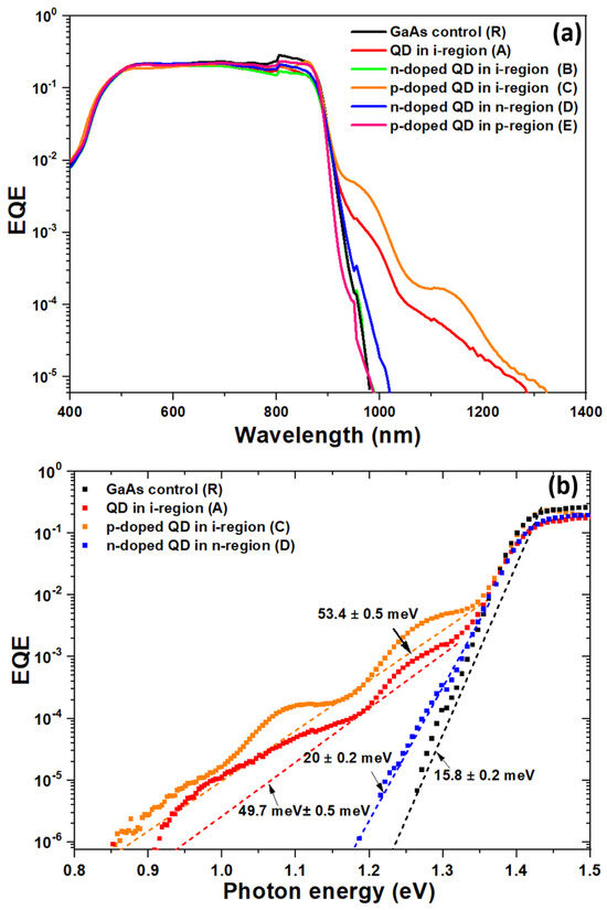
Figure 2.
(a) External quantum efficiency (EQE) of delta-doped QDSCs in depletion and (b) flat band regions with their respective Urbach tail fitting for different samples as indicated. The values show the Urbach energies. See text for details.
We used an external quantum efficiency measurement to evaluate the effect of Urbach tail in both quantum dot and bulk solar cells. An approach to derive the below-bandgap absorption in GaSb/GaAs self-assembled quantum dot devices using external quantum efficiency measurements at room temperature is presented. The measured data for the GaAs control device were fitted using the following equation:
where Eg is the bandgap energy, h is the Planck constant, ω is the photon frequency, EU is the Urbach energy and α0 is the scaling parameter. EU = (15.8 ± 0.2) meV is determined. This value is higher than 7 meV in intrinsic GaAs [6]. For the GaAs control device, the Urbach tail width is mainly determined by the doping level of the main absorption layer. The extended Urbach tail well observed with a visibly lower slope in the below-bandgap absorption region for quantum dots compared with a considerably steeper slope for the bulk solar cell in Figure 2b. To describe the tailing density of states in QD devices, the energy states of both the QD and the WL have to be considered. The curve is generated by Equation (3) with the fitted Urbach tail absorption coefficient in the following form:
where L~20 nm is the layer thickness of the dominant absorption film. From the fit, the Urbach energy for QD samples A, C and D is found to be (49.7 ± 0.3) meV, (53.4 ± 0.5) meV and (20.0 ± 0.2) meV, respectively, with all three values been larger than the GaAs Urbach energy of 15.8 meV. The αL values are then substituted in the following equation:
where ηU and ηint are the external and internal quantum efficiency. For the QD devices, the built-up strain creates disruption to the lattice, which is characterized by a much larger Urbach energy broadening. Figure 2b shows the Urbach tail fitting (dashed lines) for ηU of a control device and the quantum dot solar cells. The p-delta-doped QD sample C shows the higher Urbach energy of 53.4 meV compared to the other devices studied here. This happens when compared to the presence of defects in the depletion region where QDs are inserted, leading to open-circuit voltage reduction [7], according to equation [6], as follows:
where ηt denotes the total measured external quantum efficiency and the carrier generation efficiency via the QD and WL transition levels (ηQD&WL) can be obtained by subtracting ηU from the measured ηt. In Figure 3, the contribution of WLs and QDs is plotted based on their transition energies for all the devices.
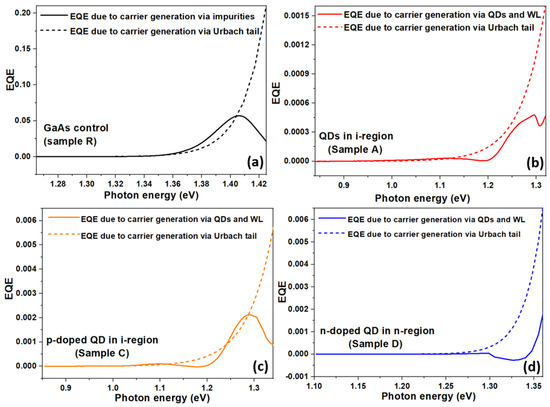
Figure 3.
EQE due to carrier generation via the Urbach tail and the QD and WL energy levels in different samples (a–d) as indicated. See text for details.
The contribution of the QD and WL to the absorption coefficient ηQD&WL is given by the following expression:
where R~0.3 is the surface reflectivity and L~20 nm. When the absorption coefficient is sufficiently small, the above equation can be further simplified:
Assuming that the internal quantum efficiency is 100% through the energy range of interest, the dependence of αQD&WL on energy can then be plotted. The absorption curve for sample A is fitted with Gaussian line shapes centered at photon energies, as shown in Figure 4. The local maxima of the first derivative were used to identify the center of the peaks to fit for QD and WL transitions.
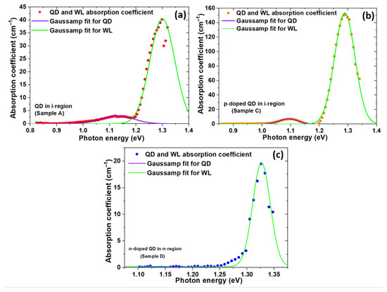
Figure 4.
Derived quantum dot and wetting layer absorption coefficient with Gaussian line shape fitting for samples A (a), C (b) and D (c).
The two transitions states of sample A are found to be centered at 1.30 eV corresponding to the WL and 1.13 eV corresponding to the QDs. Hence, the absorbance due to the transition energies for sample A is given by the following equation:
The two transition states of sample C are found to be centered at 1.29 eV, corresponding to the WL and 1.13 eV corresponding to the QDs. Hence, the absorbance due to the main transition energies is given as follows:
Similarly, the two main transition states of sample D are found to be centered at 1.33 eV, corresponding to WL and 1.17 eV corresponding to QDs. Hence, the absorbance due to the transition energies is given as follows:
The integral of the absorption coefficient over frequency for the ground state transition of the QDs is directly related to the spontaneous lifetime in QDs [6,8]:
where λ is the absorption wavelength, τsp = 1 ns [9] is the spontaneous lifetime in QD, n is the index of refraction, N is the density of QD ground states (gs) in the absorber and is twice the QD density, which is of 1.5 × 1016 cm−3. The theoretically integrated absorbance via QD ground states is therefore calculated as 1.04 × 1015 cm−1s−1, which is in reasonable agreement with the experimentally derived value of 8.1 × 1015 cm−1s−1. Therefore, the common main transition energies extracted in all the three samples are 1.3 eV for WL and 1.1 eV for GaSb QDs. Using these transition energies and the GaAs energy gap of 1.42 eV, the heavy hole confinement energies for the QDs (1.42 eV − 1.1 eV = (320 ± 20) meV) and for the WL (1.42 eV − 1.3 eV = (120 ± 10) meV) are estimated [10]. It has been reported that various factors could affect the localization energy of holes, i.e., the geometry, the GaSb/GaAs interface composition, and doping effects when relating the extended response of the solar cell with the structural characteristics of Type II quantum structures [11]. The transformation of GaSb quantum dots into ring-like structures could also alter the localization energy [12,13]. The localization energy calculated with a value of 320 meV is small compared to values previously determined for the same material system [14,15]. However, this value matches the one determined in Ref. [16]. The small hole confinement energy obtained might be because the QDs are quite small or have a relatively small Sb content at the center. In the GaSb/GaAs QD structure, the Type II band alignment provides strong hole confinement (320 ± 20 meV) but no electron confinement, which may improve carrier extraction, prevent weakening of the built-in electric field and produce a red shift of the photoresponse.
The photocurrent contributions by the sub-bandgap photons can be calculated by integrating the product of EQE and spectral irradiance of the tungsten–halogen light source [7]. We found that the extended Urbach tail accounts for 0.85% of the total short-circuit current in sample C, which is higher than in the other devices studied here. Moreover, the degradation of open circuit voltage (Voc) is related to the width of the Urbach tail, and the short circuit current (Jsc) enhancement partially comes from the Urbach tail absorption. The below-bandgap photocurrent mostly comes from the wetting layer and Urbach tail contribution, whereas the QD state contributed absorption is considerably smaller due to its quite low density and absorption coefficient. Furthermore, in this system, it has also been shown that the sub-bandgap response is limited by the thermionic emission of holes from QDs [17]. The thermal emission process is the dominant hole escape mechanism compared to tunnelling and photo-excitation in the photocurrent of our GaSb/GaAs QR solar cells. Due to the large enough valence band offset at the GaSb/GaAs QD interface, some of these holes become trapped by the QDs and must be extracted by thermal excitation in order to contribute to the external photocurrent. Moreover, the intermediate band two-photon absorption contribution to the photocurrent enhancement is quite small and is only well observable under cryogenic temperatures. Previous research used photoluminescence, photoreflectance, electroluminescence, and differential transmission measurements [17]. The fitted results obtained here are in good agreement with the results obtained via other methods [18,19].
4. Conclusions
The measurement of EQE at room temperature is used to derive the spectral dependence of QD absorption. The Urbach tail contributions from an EQE measurement for both QD and control devices at room temperature were obtained. The impact of extended Urbach tail absorption in a GaSb/GaAs QD solar cell was discussed. For a bulk GaAs device, the Urbach tail width was mainly determined by the doping level of the main absorption layer. The derived Urbach energy for the GaAs control device was (15.8 ± 0.2) meV, and for the QD devices, a much larger Urbach energy broadening of up to (53.4 ± 0.5) meV (p-doped QD device) was obtained. The analysis of below-bandgap absorption enabled a quantitative determination of the transition energies in QDs and in the WL. The theoretically integrated absorbance through QD ground states is calculated to be 1.04 × 1015 cm−1s−1, showing a satisfactory alignment with the experimental value of 8.1 × 1015 cm−1s−1. Consequently, the primary transition energies identified across all three samples are 1.3 eV for WL and 1.1 eV for GaSb QDs. Using the transition energies, the heavy hole confinement energies for the QDs ((320 ± 20) meV) and for the WL ((120 ± 10) meV) are estimated and compared. The advantage of this method is that it gives the absorption strength of QDs and WL transition levels directly. Potentially, an even higher resolution can be obtained by taking the measurements at lower temperatures. We believe this study could pave the way for the realization of an intermediate band solar cell because the spatial separation of electron and holes can be engineered provided that an intermediate band is closer to the theoretical optimum and reduces unwanted thermal emission and capture processes.
Author Contributions
methodology, J.S.J., H.F., A.R.J.M. and A.K.; validation, A.K.; formal analysis, P.J.C. and S.K.; investigation, S.K. and A.K.; resources, J.S.J. and H.F.; writing—original draft, J.S.J.; writing—review & editing, J.S.J., P.J.C. and A.K.; supervision, A.K. All authors have read and agreed to the published version of the manuscript.
Funding
Financial support for this work was provided by the EU Marie-Curie Training networks PROPHET (PITN-GA-2010-264687). H.F. would like to thank Asahi Kasei Corporation for the award of an industry scholarship. A.R.J.M. and P.J.C. gratefully acknowledge support of fellowships from the Royal Academy of Engineering, UK (grant number 10216/114).
Data Availability Statement
The raw data supporting the conclusions of this article will be made available by the authors on request.
Acknowledgments
We would like to express our sincere gratitude to Lancaster University, UK, for providing access to necessary research materials and resources that greatly facilitated our study.
Conflicts of Interest
Hiromi Fujita is a member of Asahi Kasei Corporation. The remaining authors declare that the research was conducted in the absence of any commercial or financial relationships that could be construed as a potential conflict of interest.
References
- Hwang, J.; Martin, A.J.; Millunchick, J.M.; Phillips, J.D. Thermal emission in type-II GaSb/GaAs quantum dots and prospects for intermediate band solar energy conversion. J. Appl. Phys. 2012, 111, 074514. [Google Scholar] [CrossRef]
- Ramiro, I.; Villa, J.; Tablero, C.; Antolin, E.; Luque, A.; Marti, A.; Hwang, J.; Phillips, J.; Martin, A.J.; Millunchick, J. Analysis of the intermediate-band absorption properties of type-II GaSb/GaAs quantum-dot photovoltaics. Phys. Rev. B 2017, 96, 125422. [Google Scholar] [CrossRef]
- Shojia, Y.; Tamaki, R.; Okada, Y. Multi-stacked GaSb/GaAs type-II quantum nanostructures for application to intermediate band solar cells. AIP Adv. 2017, 7, 065305. [Google Scholar] [CrossRef]
- Carrington, P.J.; Montesdeoca, D.; Fujita, H.; James, J.; Wagener, M.C.; Botha, J.R.; Marshall, A.R.J.; Krier, A. Type II GaSb/GaAs quantum rings with extended photoresponse for efficient solar cells. In Proceedings SPIE 9937: Next Generation Technologies for Solar Energy Conversion VII; Sulima, O.V., Conebeer, G., Eds.; SPIE Digital Library: Bellingham, WA, USA, 2016; p. 993708. [Google Scholar] [CrossRef]
- Carrington, P.J.; Wagener, M.C.; Botha, J.R.; Sanchez, A.M.; Krier, A. Enhanced infrared photo-response from GaSb/GaAs quantum ring solar cells. Appl. Phys. Lett. 2012, 101, 231101. [Google Scholar] [CrossRef]
- Li, T.; Dagenais, M. Below-bandgap absorption in InAs/GaAs self-assembled quantum dot solar cells. Prog. Photovolt. Res. Appl. 2014, 23, 997–1002. [Google Scholar] [CrossRef]
- Asirvatham, J.S.J.; Fujita, H.; Fernández-Delgado, N.; Herrera, M.; Molina, S.I.; Marshall, A.R.J.; Krier, A. Delta doping and positioning effects of type II GaSb quantum dots in GaAs solar cell. Mater. Res. Innov. 2015, 19, 512–516. [Google Scholar] [CrossRef]
- Birkedal, D.; Bloch, J.; Shah, J.; Pfeiffer, L.N.; West, K. Femtosecond dynamics and absorbance of self-organized InAs quantum dots emitting near 1.3 μm at room temperature. Appl. Phys. Lett. 2000, 77, 2201–2203. [Google Scholar] [CrossRef]
- Harbord, E.; Spencer, P.; Clarke, E.; Murray, R. Radiative lifetimes in undoped and p-doped InAs/GaAs quantum dots. Phys. Rev. B 2009, 80, 195312. [Google Scholar] [CrossRef]
- Alonso-Álvarez, D.; Alén, B.; García, J.M.; Ripalda, J.M. Optical investigation of type II GaSb/GaAs self-assembled quantum dots. Appl. Phys. Lett. 2007, 91, 263103. [Google Scholar] [CrossRef]
- Bimberg, D.; Grundmann, M.; Ledentsov, N.N. Quantum Dot Heterostructures; John Wiley & Sons Ltd.: Chichester, UK, 2001; Available online: https://archive.org/details/quantumdothetero0000bimb (accessed on 21 June 2024).
- Martin, A.J.; Hwang, J.; Marquis, E.A.; Smakman, E.; Saucer, T.W.; Rodriguez, G.V.; Hunter, A.H.; Sih, V.; Koenraad, P.M.; Phillips, J.D.; et al. The disintegration of GaSb/GaAs nanostructures upon capping. Appl. Phys. Lett. 2013, 102, 113103. [Google Scholar] [CrossRef]
- Wagener, M.C.; Carrington, P.J.; Botha, J.R.; Krier, A. Simulation of the enhanced infrared photoresponse of type-II GaSb/GaAs quantum ring solar cells. Appl. Phys. Lett. 2013, 103, 063902. [Google Scholar] [CrossRef]
- Geller, M.; Kapteyn, C.; Muller-Kirsch, L.; Heitz, R.; Bimberg, D. 450 meV hole localization in GaSb/GaAs quantum dots. Appl. Phys. Lett. 2003, 82, 2706–2708. [Google Scholar] [CrossRef]
- Nowozin, T.; Marent, A.; Bonato, L.; Schliwa, A.; Bimberg, D.; Smakman, E.P.; Garleff, J.K.; Koenraad, P.M.; Young, R.J.; Hayne, M. Linking structural and electronic properties of high-purity self-assembled GaSb/GaAs quantum dots. Phys. Rev. B 2012, 86, 035305. [Google Scholar] [CrossRef]
- Nowozin, T.; Wiengarten, A.; Bonato, L.; Bimberg, D.; Lin, W.-H.; Lin, S.-Y.; Ajour, M.N.; Daqrouq, K.; Balamesh, A.S. Electronic properties and density of states of self-assembled GaSb/GaAs quantum dots. J. Nanotechnol. 2013, 2013, 302647. [Google Scholar] [CrossRef]
- Cánovas, E.; Martí, A.; Fuertes Marrón, D.; Antolín, E.; Linares, P.G.; Luque, A.; Farmer, C.D.; Stanley, C.R. Optical characterization of quantum dot intermediate band solar cells. In The Compiled State-of-the-Art of PV Solar Technology and Deployment. 23rd European Photovoltaic Solar Energy Conference, EU PVSEC 2008. Proceedings; WIP-Renewable Energies: Munich, Germany, 2008; pp. 298–301. Available online: https://oa.upm.es/3579/ (accessed on 21 June 2024).
- Hatami, F.; Grundmann, M.; Ledentsov, N.N.; Heinrichsdor, F.; Heitz, R.; Böhrer, J.; Bimberg, D.; Ruvimov, S.S.; Werner, P.; Ustinov, V.M.; et al. Carrier dynamics in type-II GaSb/GaAs quantum dots. Phys. Rev. B 1998, 57, 4635–4641. [Google Scholar] [CrossRef]
- Tatebayashi, J.; Liang, B.; Bussian, D.A.; Htoon, H.; Huang, S.; Balakrishnan, G.; Klimov, V.; Dawson, L.R.; Huffaker, D.L. Formation and optical characteristics of type-II strain-relieved GaSb/GaAs quantum dots by using an interfacial misfit growth mode. IEEE Transact. Nanotechnol. 2008, 8, 268–274. [Google Scholar] [CrossRef]
Disclaimer/Publisher’s Note: The statements, opinions and data contained in all publications are solely those of the individual author(s) and contributor(s) and not of MDPI and/or the editor(s). MDPI and/or the editor(s) disclaim responsibility for any injury to people or property resulting from any ideas, methods, instructions or products referred to in the content. |
© 2024 by the authors. Licensee MDPI, Basel, Switzerland. This article is an open access article distributed under the terms and conditions of the Creative Commons Attribution (CC BY) license (https://creativecommons.org/licenses/by/4.0/).