Abstract
A symmetric laser beam pair can provide unique control over light–matter interactions. When propagating within a symmetric slab waveguide, its non-conical diffraction at a specially designed symmetric leaky waveguide grating can be completely suppressed, a phenomenon we term zero diffraction. This allows for infinite contrast control of light detrapping from the slab waveguide. In this paper, we demonstrate the electric control of the local deflection of a beam pair while preserving its properties. This introduces a novel method for routing optical signals across a planar waveguide. We utilize a waveguide structure that enables zero diffraction under non-conical incidence on a 1D grating and design a grating geometry capable of deflecting the beam pair by approximately 90 degrees. This design is experimentally realized using three different diffractive elements for trapping, deflection, and detrapping. The deflection is controlled by an electric field, allowing the deflected intensity to be tuned by a factor of 21.
1. Introduction
Actively controlling the geometric path of light is a key challenge in optics, with applications in communication, imaging, and information processing. In these contexts, routing light to a localized spot within an area is often crucial for efficient information transfers [1,2,3]. Various applications in this field include optical wiring, photonic interconnects, quantum optics [1], optical signal processing [2], displays [4], holography [5], and Light Detection and Ranging (LIDAR) [6]. In free-space optics, dynamic beam steering and spatial light modulation are established solutions for geometric light control, showing promising applications in display and LIDAR technologies. Notable examples include Digital Micromirror Devices (DMDs), which offer low losses from the reflected beam and high deflection angles. However, the flatness of MEMS mirrors is limited by manufacturing technology, and high scanning speeds cause bending due to high acceleration forces [7,8,9]. Liquid Crystal on Silicon (LCoS) is an emerging technology for augmented reality but faces challenges regarding further miniaturization [4,10]. Reconfigurable metasurfaces [11,12] show promise for display [13,14] and LIDAR [6] applications.
Despite these advancements, effective methods to geometrically manipulate guided light within waveguides remain limited. While modulating the optical phase in waveguides by electro-optic effects is well established [15,16], the active and repeatable redirection of guided light’s path remains a challenge.
In stripe waveguides, Mach–Zehnder interferometer (MZI) switches utilize the phase differences between two arms controlled by thermo-optic [17] or electro-optic effects [18] to switch between different output ports with extinction ratios of about 40 dB. This method can be used for geometrical control, but is limited by structural complexity and deflection positions which are defined by the structure. Applications such as information processing or display technologies require high-density integration featuring numerous controllable intersections [19,20]. As the number of switches increases, precise structuring becomes critical. Additionally, factors such as optical loss and crosstalk noise become significant constraints on scalability [21].
Slab waveguides with less complex structuring offer an additional degree of freedom, potentially enabling freely selectable deflection positions, but there are limited approaches to deflect guided light within the plane efficiently. One method utilizes photo-induced birefringence to switch the diffraction efficiency of an optical grating, which deflects light within the plane of a slab waveguide at an angle of 30 degrees [22].
In a recent publication, we showed the promising switching behavior of a symmetric laser beam pair guided in a special slab waveguide. During single interactions with a center waveguide grating, light is either allowed to exit the waveguide through diffraction or remains confined with zero diffraction, demonstrating the full control of detrapping in a symmetric slab waveguide. The diffraction efficiency is controlled by tuning the relative phase using the electro-optic Pockels effect [23].
Tuning the relative phases of two separate, independently adjusted beams has been employed to continuously control interactions [24,25]. Here, the emergence of a symmetric beam pair is a direct result of the symmetry within the waveguide structure. Consequently, there is no requirement for the independent adjustment of the two beams. Additionally, due to the symmetry of the slab waveguide, ambient conditions such as pressure and temperature affect both beams equally, thereby suppressing environmental influences.
However, high-contrast switching demands a perfectly symmetric beam pair propagating through the slab waveguide. Thus, the method’s applicability is limited, as it only allows for switching at certain specific positions along the straight-line propagation path. Our goal is to enable controlled detrapping throughout the entire area of a slab waveguide by actively deflecting the beam pair within the plane of the waveguide. The optimal setup would permit the accurate deflection of a beam pair with controllable efficiency within the waveguide’s plane, ensuring both vertical confinement and the preservation of the beam pair’s symmetric characteristics. Residual light continues its propagation within the slab waveguide and may be deflected through further interactions. This approach would enable light to be directed to any location in the waveguide’s area, offering a method with a much lower form factor compared to existing technologies and, simultaneously, a less complex structure.
We present the controlled in-plane deflection of symmetric beam pairs, while preserving their vertical confinement within a slab waveguide. As the first study on this topic, we consider whether modifying the waveguide grating, specifically by changing the lateral angle, provides a viable method for in-plane light routing while preserving the symmetric properties of a beam pair, which is necessary for zero diffraction.
2. Results and Discussion
2.1. A Concept for Detrapping a Symmetric Beam Pair from a Slab Waveguide after Controlled In-Plane Deflection
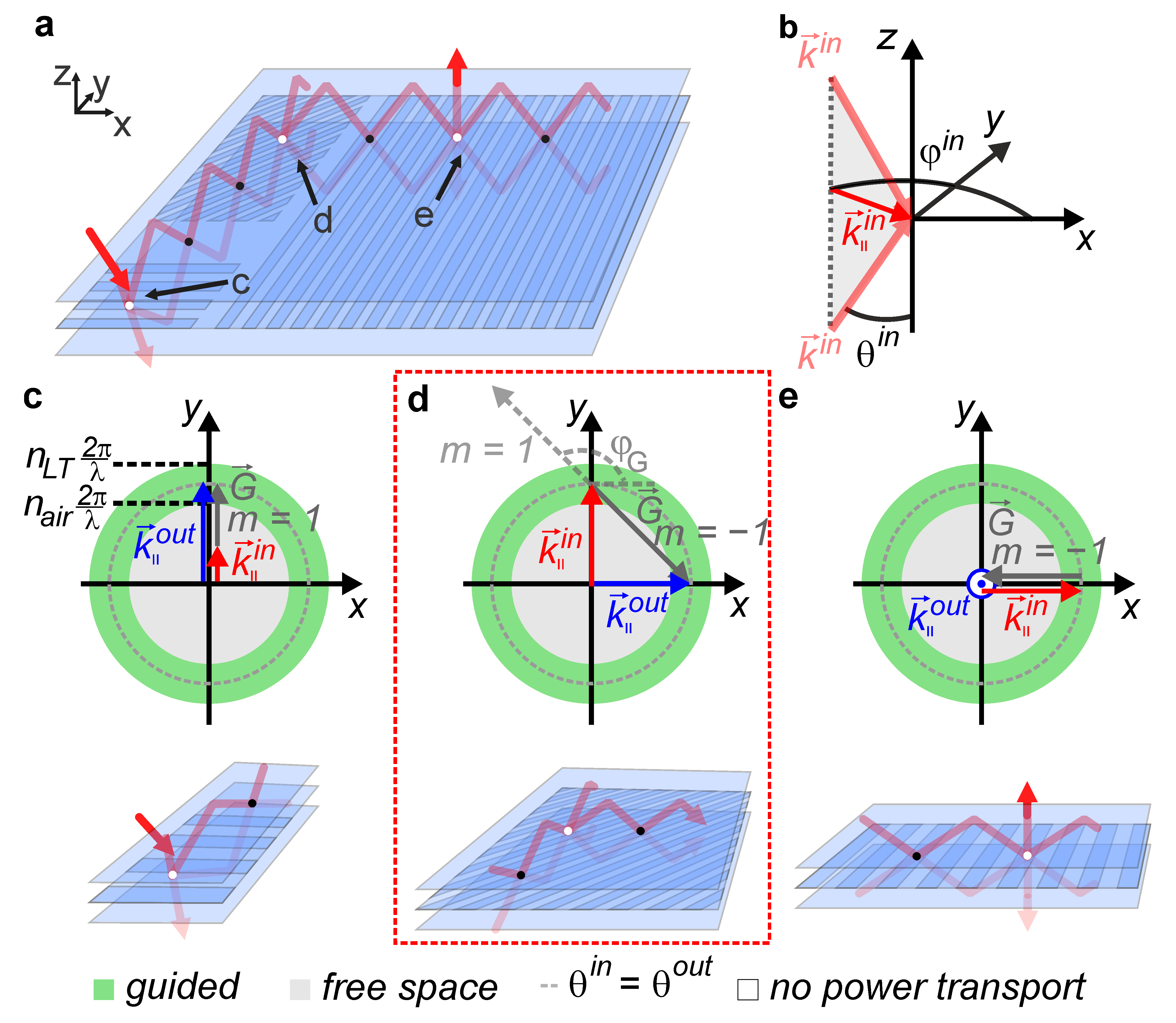
The concept consists of three steps (Figure 1a). A symmetrical beam pair is formed by trapping, as shown in Figure 1c, which involves incoupling, the leveling of amplitudes, and a phase shift. After controlled in-plane deflection (Figure 1d) at a desired position, the beam pair is detrapped (Figure 1e) at a single position on the area of the slab waveguide [26]. All of these steps are based on a symmetrical waveguide with a leaky waveguide grating at the center and electric control of the relative phase of a symmetrical beam pair.

Figure 1.
Illustration of the concept featuring controlled in-plane deflection. (a) Simplified representation of a slab waveguide by its interfaces and a guided beam pair. Interactions with the grating are indicated by black dots (suppressed) or white dots (enhanced). (b) Definition of the used spherical coordinate system with the vector of incoming waves at an azimuthal angle , polar angle , and lateral vector , (c) illustration of the lateral momentum before () and after () transfer, characterized by the addition of vector at diffraction order m, for trapping (d) deflection with the grating’s rotation angle and (e) detrapping.
The depiction of the slab waveguide is simplified by its outer boundaries. The waveguide grating’s center represents a mirror symmetry plane. Setting this symmetry plane as the origin, the complex refractive indices follow: (n(z) = n(−z)). Further, the slab waveguide contains gratings with different grating periods and orientations. In the outer layers of the waveguide, the relative phase of the symmetric beam pair is detuned, thereby suppressing the interaction with the waveguide grating. Afterwards, the beam pair propagates almost undisturbed (black dots). By reverting the relative phase to its initial state, the interaction becomes enhanced (white dots).
For many applications, an orthogonal deflection is favorable because it results in a rectangular matrix of individually switchable positions. While deflection defines rows, detrapping defines the columns. Unlike trapping and detrapping, deflection involves a grating vector, which is rotated in the symmetry plane, and therefore requires a conical description with challenging mathematics. This complexity poses difficulties for methods such as RCWA (rigorous coupled wave analysis) or numeric calculations. However, the interaction must comply with the conservation of momentum, which can be represented graphically.
In general, a plane wave can be described by a wave vector. Figure 1b illustrates the vectors of a beam pair incident on the waveguide grating, defined by the azimuthal angle and the polar angle . These vectors can be decomposed into a lateral vector and a vertical vector . The incident vectors can be expressed as follows:
Due to the symmetry, the beam pair is fully defined by one lateral wave vector along with the refractive index. The individual beams of the pair differ only in the sign of their z-component. For the resulting wave vector after the interaction (), a similar decomposition occurs.
With the grating vector , the momentum transfer of a waveguide grating can be represented in the x–y plane:
The value of the wave vector is given by , where represents the refractive index of the medium in which the wave propagates. In the context of this work, considerations refer to the refractive index of lithium tantalate . The value of the full wave vectors inside the medium before and after the interaction needs to be equal, with . A change in lateral momentum directly affects the z-component and the azimuthal angle . The addition of the grating vector introduces a shift between the components, resulting in a change in direction.
Figure 1c to e depict the vector combination of lateral vectors in the x-y plane. Considering the conditions for total internal reflection, where , the green region represents the allowed range of beam pairs guided inside the waveguide. The inner gray disk defines the range of free-space wave vectors that can exit or enter the waveguide. Light waves with a resulting momentum outside the green region cannot propagate within the waveguide. The associated wave vector becomes purely imaginary. These waves are evanescently coupled, and no power transport occurs.
- Trapping
In Figure 1c, one single beam incident from the outside with vector is trapped into the waveguide. The trapped symmetric beam pair propagates with the vector in the y direction.
- Deflection
Figure 1d depicts the special case of a 90 deg deflection of this beam pair, which is incident on a waveguide grating with the vector . With the diffraction order , the grating period and the grating’s rotation angle relative to the x-axis ( 135 deg) are chosen such that the lateral momentum after diffraction is given by:
This corresponds to a deflection of 90 deg while maintaining a constant magnitude of the lateral momentum. The azimuthal angle stays unchanged (sketched by a gray dashed circle). A suitable azimuthal angle is essential for zero diffraction. Consequently, the interaction with the waveguide grating can again be suppressed. Afterwards, the deflected beam pair propagates almost undisturbed.
- Detrapping
Along the generated parallel propagation paths (rows) light can be extracted at controlled local positions (Figure 1e). The grating vector is chosen through the grating period such that the resulting vector has no lateral component, , and propagates with an azimuthal angle of = 0 deg in the z direction (gray disk).
Combining the deflection and detrapping of a symmetric beam pair, a matrix of single switchable positions is achieved. In the following section, we discuss the details required to achieve an orthogonal deflection.
2.2. Visualizing the Impact of Grating Geometry on the In-Plane Deflection of Beam Pairs
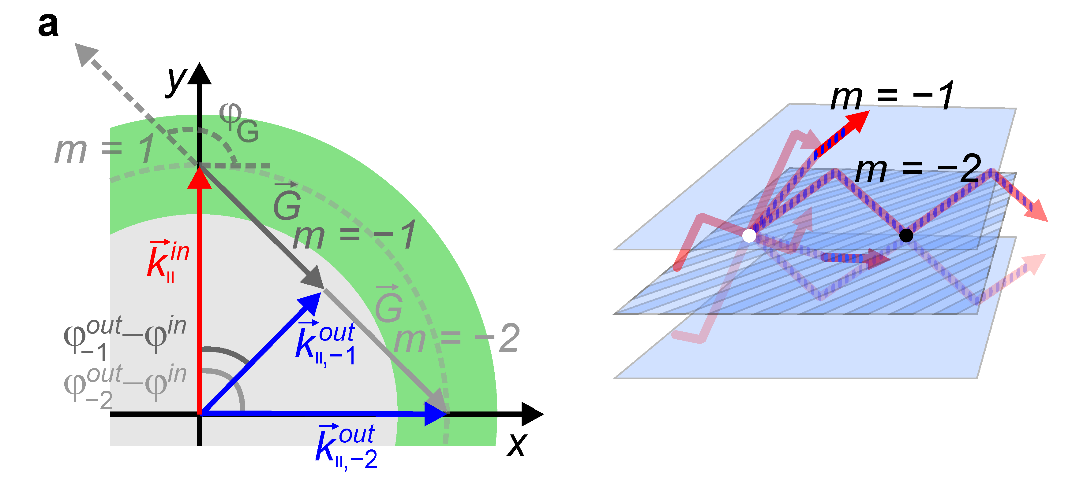
In order to achieve precise deflection, it is crucial to adjust the grating vector accordingly. We elaborate on this by presenting the momentum in more detail in Figure 2 and examine a few examples of grating structures that must be avoided for the intended application.
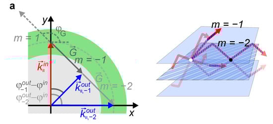
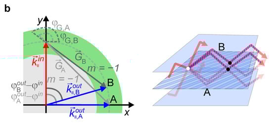
Figure 2.
Impact of grating geometry: (a) reduced value of the grating vector with two resulting beam pairs; (b) orthogonal (A) and almost orthogonal (B) deflection, both maintaining the azimuthal angle.
In Figure 2a, the decreased value of the grating vector leads to the separate deflection of two beam pairs. The beam pair associated with the diffraction order in the gray area is deflected by 45 deg and leaves the waveguide laterally at 45 deg, whereas the beam pair persists within the green region with 90 deg. Conversely, the diffraction order remains evanescently coupled, leading to no power transport. This scenario presents two undesired outcomes: an outcoupled beam pair and the presence of two permissible diffraction orders. For controlled in-plane deflection, it is preferable to use a structure that allows only a single diffraction order. All diffraction orders, except for the required one, are intended to be evanescently coupled.
Figure 2b illustrates an orthogonal deflection with the desired constant azimuthal angle (marked as A). To achieve a deflection angle, 90 deg adjustments to the grating period and the grating angle are necessary, as shown for a marginally decreased deflection angle, marked as B.
In subsequent experiments, we employed optical gratings obtained from commercial sources, which are characterized by a fixed grating period. A deflection angle was realized while maintaining the azimuthal angle.
In summary, deflecting a symmetric beam pair and maintaining vertical confinement in various directions is possible, including a deflection of 90 deg. To maintain the azimuthal angle, it is crucial to adjust both the grating period and the grating angle. Both components of a beam pair are described by the value of the wave vector. The refractive index symmetry of the slab waveguide enforces the symmetry of the beam pair concerning its azimuthal angle. The deflection will be verified in the following experiment.
2.3. Experimental Observation of Controlled Deflection
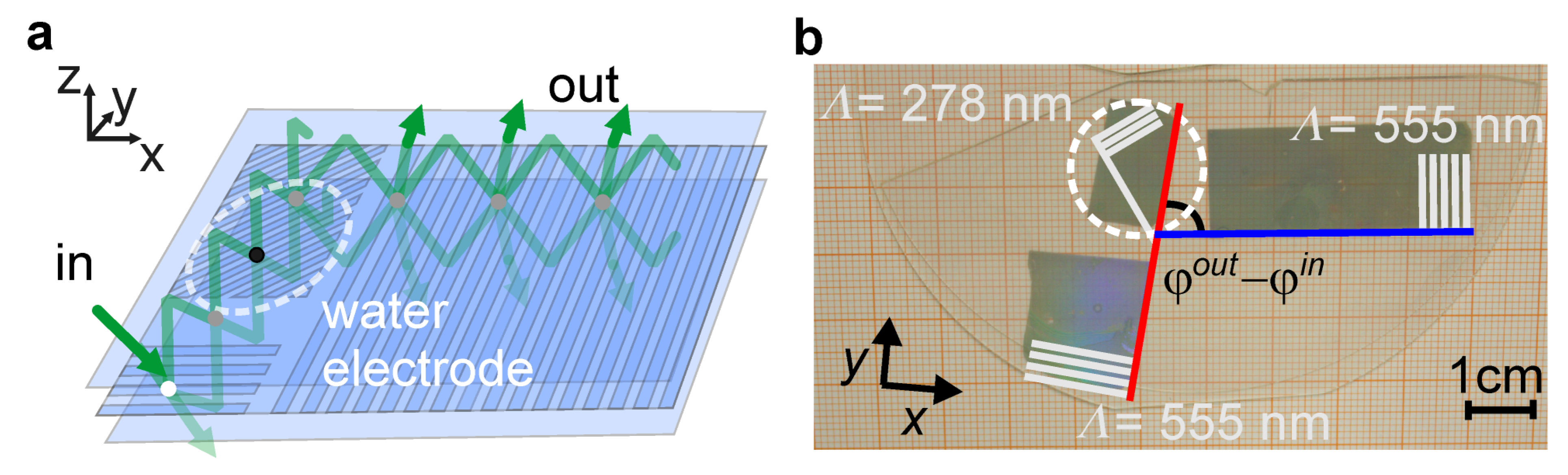
To validate the theoretical models, we fabricated device stacks designed for in-plane deflection. A 4-inch lithium tantalate wafer with a thickness of µm was pretreated with an excimer irradiation ( nm) at a dose of approximately 25 J/m2. This process aimed to increase the surface energy to enhance the wetting properties of the polymer solution [27]. Subsequently, the wafer was coated with a 1 µm thick layer of Ormocore by spin coating, using a solution composed of propylene glycol methyl ether acetate (PGMEA) and Ormocore. Following a vacuum treatment ( mbar, duration min), the coated wafer was cut in two halves, and each half was UV-cured separately.
The first half received a full UV cure ( nm) with a dose of approximately 2 J/m2, while the second half was cured with only 10% of this dose. The reduced dose served to increase the viscosity, thereby decreasing the dewetting of the Ormocore layer. On the surface of the fully cured half, a silver grating was transfer printed [28,29]. To achieve this, standard sinusoidal gratings with periods of nm and nm were replicated in polydimethylsiloxane (PDMS). The PDMS replica was then coated with silver (Ag) at a deposition angle of 50 deg. The standard sinusoidal gratings with the period nm possess an amplitude of 40 nm. Thus, to prevent the formation of a continuous silver film, the deposition is limited to a height of 30 nm. This silver film was subsequently transferred. Finally, both halves of the substrate were laminated together under a lab press (p = 50 bar) and simultaneously UV cured ( nm) with a dose of approximately 2 J/m2. This process resulted in the formation of a symmetric stack comprising LiTaO3/Ormocore/grating/Ormocore/LiTaO3.
In Figure 3a, we present a sketch of the experiment. Green laser light (λ = 532 nm, θ < 1.5 mrad) was coupled into the waveguide through an optical grating (Λ = 555 nm) and propagated in the y direction. The generated beam pair traveled through the waveguide with the azimuthal angle and interacted with a deflection grating ( nm; deg), being deflected to the x-direction by an angle of 81.3 deg. Figure 3b shows a photograph of the fabricated waveguide. Through symmetric lamination, the two layers of lithium tantalate µm became orientated in the opposite direction to the c-axis. When a voltage was applied, a phase difference was induced within the beam pair. The relative phase shift caused by the electric field can be determined using Equation (4).
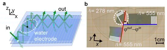
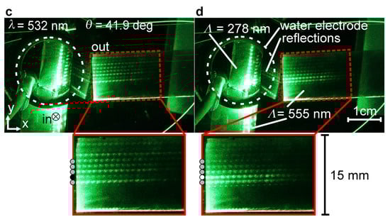
Figure 3.
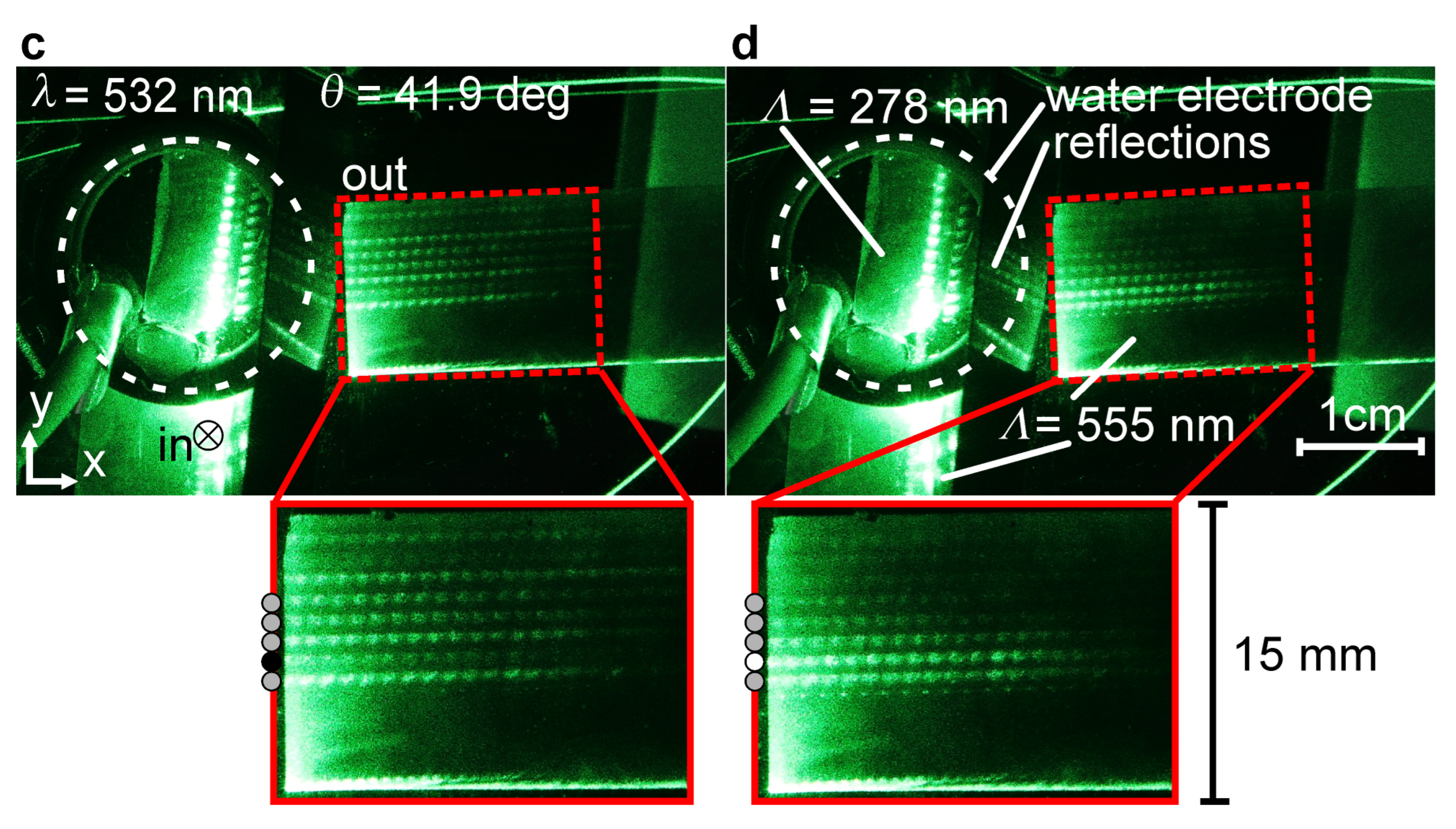
Experiment for controlled in-plane deflection. A slab waveguide features three distinct gratings: two for diffraction into and out of the waveguide ( nm) and a grating for deflection ( nm) A laser beam ( nm; mm) is diffracted into the slab waveguide. An electric field is applied using water electrodes. (a) Sketch; (b) photograph of a slab waveguide and (c) suppressed deflection at the second point of interaction (black dot); (d) enhanced deflection at the second interaction (white dot).
TE polarization was employed, and the effective Pockels coefficient was pm/V [30,31]. Consequently, a difference in electric field strength of ΔE V/mm is required for a relative phase shift of .
In the first experimental demonstration, the electric field was applied across the entire waveguide, requiring high voltages. Within the region of the deflection grating, a circular water electrode with a diameter (d) of 2 cm was placed on the outside of the waveguide. This very simple single electrode geometry was chosen to avoid electrical breakdowns. Our study aims to demonstrate independent control of deflection. Because controlled detrapping has already been investigated, the relative phase on the third grating (enabling detrapping with a grating period of Λ = 555 nm and visualizing the beam) is not actively tuned. Controlled interactions are labeled with black (suppressed) or white (enhanced) dots, while interactions with uncontrolled phase are labeled with gray dots.
In Figure 3c, the deflection at the second point of interaction is suppressed at a field strength of V/mm. In contrast, in Figure 3d, this interaction is enhanced with a field strength of V/mm. The electric field difference matches the expected value. The individual rows can be selectively manipulated using electric control, as also demonstrated in Supporting Video S1.
To assess the controllability of the deflection, we conducted measurements using a Charged-Coupled-Device camera (CCD, Ximea MD120MU-SY). We incrementally applied an electric field ranging from V/mm to V/mm in in steps of V/mm. Through electrical control, we reduced the brightness of row 1 to 4.7% of its original value, while row 2 was reduced to 6.2% of its original value. All measurements were corrected for a dark current, resulting in contrast factors of the two rows of approximately 21 and 15, respectively. In the Supporting Information, a similar experiment using red laser light (λ = 633 nm) and an adjusted slab waveguide structure is provided.
These contrast values are smaller compared to the values greater than 1000 found for detrapping. However, this is likely due to the increased light scattering that occurred on the transfer-printed silver grating with a decreasing grating period. Since the deflection grating requires a period half the size of the detrapping grating, its realization is much more challenging using our transfer printing technique [28,29]. Future studies will focus on dielectric, loss-free gratings that are fully compatible with zero diffraction [23]. These gratings will be produced using nanoimprint lithography [32,33,34]. Additionally, we aim to reduce the operating voltage and increase the scalability of our approach. A potential solution could involve looking into the non-linear effects of thin films or non-crystalline materials, which have the potential to contribute significantly [35,36,37,38]. Also, the utilization of metasurfaces with optical responses tailored to specific illumination conditions could enhance the scalability of the procedure and facilitate its operation at lower voltages [39,40].
3. Conclusions
We developed and studied the concept of in-plane deflection, demonstrating that a symmetrical beam pair can be deflected within the plane while remaining confined in the vertical dimension. In first experiments, the intensity of these parallel straight-propagating rows was modulated by adjusting their relative phase.
Building on this foundation, our method presents exciting synergies with our previously published detrapping method, offering the possibility to generate a pixel matrix. This principle has promising applications in on-chip scanning and projection systems, potentially inspiring communication technologies such as information displays and projectors. These applications require several controllable interactions. Through the generation of rows and columns, necessary interactions are reduced to a minimum along with structuring complexity and cost. Scalability is a critical challenge for photonic interconnections. Thus, this novel method for routing light across a planar waveguide might open a new avenue for photonic information processing. Addressing the scalability challenges is an aspect of our ongoing research. Additionally, the form factor of this method is significantly reduced compared to free-space methods, as light is guided and deflected within a slab waveguide.
However, there are challenges for this new method that are aspects of our ongoing research. The operation voltage needs to be reduced, and scalability beyond the size of a monocrystalline wafer must be addressed. Both challenges are related to the choice of material and the effect of phase switching.
Supplementary Materials
The following supporting information can be downloaded at: https://www.mdpi.com/article/10.3390/opt5030025/s1, Figure S1: Experiment for controlled in-plane deflection using red laser light ( nm). The deflection grating is adjusted for the wavelength with a grating period Λ = 333 nm and a deflection angle deg. (a) Photograph of a slab waveguide with an applied field strength of V/mm, (b) V/mm, and (c) measurement of the detrapped power during the first interaction; Video S1: Experiment for controlled in-plane deflection.
Author Contributions
Conceptualization, A.H. and P.G.; methodology, A.H. and P.G.; validation, A.H., C.K., M.B. and P.G.; formal analysis, A.H. and P.G.; investigation, A.H. and P.G.; resources, P.G.; data curation, A.H.; writing—original draft preparation, A.H.; writing—review and editing, A.H., C.K., M.B. and P.G; visualization, A.H.; supervision, P.G.; project administration, P.G.; funding acquisition, P.G. All authors have read and agreed to the published version of the manuscript.
Funding
For financial support, this project received funding from the European Research Council (ERC) under the European Union’s Horizon 2020 research and innovation program (Grant Agreement No. 637367), as well as the Federal Ministry of Education and Research (Photonics Research Germany funding program, Contract No. 13N15390).
Data Availability Statement
The data in this study are available on request from the corresponding author.
Acknowledgments
We utilized AI-assisted technology for language editing, specifically OpenAI’s ChatGPT.
Conflicts of Interest
The authors declare no conflicts of interest.
References
- Mehta, K.K.; Bruzewicz, C.D.; Mcconnell, R.; Ram, R.J.; Sage, J.M.; Chiaverini, J. Integrated Optical Addressing of an Ion Qubit. Nat. Nanotechnol. 2016, 11, 1066–1070. [Google Scholar] [CrossRef] [PubMed]
- Cheben, P.; Halir, R.; Schmid, J.H.; Atwater, H.A.; Smith, D.R. Subwavelength Integrated Photonics. Nature 2018, 560, 565–572. [Google Scholar] [CrossRef]
- Meng, Y.; Chen, Y.; Lu, L.; Ding, Y.; Cusano, A.; Fan, J.A.; Hu, Q.; Wang, K.; Xie, Z.; Liu, Z.; et al. Optical Meta-Waveguides for Integrated Photonics and Beyond. Light. Sci. Appl. 2021, 10, 235. [Google Scholar] [CrossRef] [PubMed]
- Huang, Y.; Liao, E.; Chen, R.; Shin-Tson, W. Liquid-Crystal-on-Silicon for Augmented Reality Displays. Appl. Sci. 2018, 8, 2366. [Google Scholar] [CrossRef]
- Smalley, D.E.; Smithwick, Q.Y.J.; Bove, V.M.; Barabas, J.; Jolly, S. Anisotropic Leaky-Mode Modulator for Holographic Video Displays. Nature 2013, 498, 313–317. [Google Scholar] [CrossRef] [PubMed]
- Park, J.; Jeong, B.G.; Kim, S.I.; Lee, D.; Kim, J.; Shin, C.; Lee, C.B.; Otsuka, T.; Kyoung, J.; Kim, S.; et al. All-Solid-State Spatial Light Modulator with Independent Phase and Amplitude Control for Three-Dimensional LiDAR Applications. Nat. Nanotechnol. 2021, 16, 69–76. [Google Scholar] [CrossRef]
- Van Kessel, P.; Hornbeck, L.; Meier, R.; Douglass, M. MEMS-Based Projection Display. SPIE Crit. Rev. 1989, 1150, 86–102. [Google Scholar] [CrossRef]
- Kruger, S.; Kamps, J.; Wernicke, G.; Gruber, H.; Demoi, N.; Dürr, M.; Teiwes, S. Spatial Light Modulator System for the Application as Dynamic Diffractive Element and in Optical Image Processing. In Proceedings of the Diffractive/Holographic Technologies and Spatial Light Modulators VII, San Jose, CA, USA, 10 March 2000; p. 3951. [Google Scholar]
- Dobosz, M. Reflection Techniques of Continuous Laser Beam Deflection—A Comprehensive Overview. Precis. Eng. 2024, 88, 644–655. [Google Scholar] [CrossRef]
- Johnson, K.M.; McKnight, D.J.; Underwood, I. Smart Spatial Light Modulators Using Liquid Crystals on Silicon. IEEE J. Quantum Electron. 1993, 29, 699–714. [Google Scholar] [CrossRef]
- Gu, T.; Kim, H.J.; Rivero-Baleine, C.; Hu, J. Reconfigurable Metasurfaces towards Commercial Success. Nat. Photonics 2023, 17, 48–58. [Google Scholar] [CrossRef]
- Zhang, Z.; Shi, H.; Wang, L.; Chen, J.; Chen, X.; Yi, J.; Zhang, A.; Liu, H. Recent Advances in Reconfigurable Metasurfaces: Principle and Applications. Nanomaterials 2023, 13, 534. [Google Scholar] [CrossRef]
- Kim, G.; Kim, S.; Kim, H.; Lee, J.; Badloe, T.; Rho, J. Metasurface-Empowered Spectral and Spatial Light Modulation for Disruptive Holographic Displays. Nanoscale 2022, 14, 4380–4410. [Google Scholar] [CrossRef]
- Li, J.; Yu, P.; Zhang, S.; Liu, N. Electrically-Controlled Digital Metasurface Device for Light Projection Displays. Nat. Commun. 2020, 11, 3574. [Google Scholar] [CrossRef] [PubMed]
- Liu, K.; Ye, C.R.; Khan, S.; Sorger, V.J. Review and Perspective on Ultrafast Wavelength-Size Electro-Optic Modulators. Laser Photonics Rev. 2015, 9, 172–194. [Google Scholar] [CrossRef]
- Li, M.; Ling, J.; He, Y.; Javid, U.A.; Xue, S.; Lin, Q. Lithium Niobate Photonic-Crystal Electro-Optic Modulator. Nat. Commun. 2020, 11, 4123. [Google Scholar] [CrossRef]
- Shijie, S.; Xueqing, S.; Tianhang, L.; Yuanhua, C.; Zhu, M.; Yu, Q.; Xie, Y.; Xibin, W.; Daming, Z. 1 × 2 Mode-Independent Polymeric Thermo-Optic Switch Based on a Mach–Zehnder Interferometer with a Multimode Interferometer. Opt. Express 2023, 56, 8164–8168. [Google Scholar]
- Wang, Z.; Xiang, M.; Yang, F.; Liu, K.; Bao, J.; Yang, D.; Wang, Y. Ultrafast and High Extinction Ratio 1×4 Electro-Optical Switch Based on Cascaded Dual-Output MZI. IEEE Photonics J. 2023, 15, 1–8. [Google Scholar] [CrossRef]
- Zhu, X.; Wang, X.; Huang, Y.; Wu, L.; Zhao, C.; Xiao, M.; Wang, L.; Davidson, R.; Ou, Y.; Little, B.E.; et al. Low-Loss and Polarization Insensitive 32 × 4 Optical Switch for ROADM Applications. Light. Sci. Appl. 2024, 13, 94. [Google Scholar] [CrossRef] [PubMed]
- Zhu, H.H.; Zou, J.; Zhang, H.; Shi, Y.Z.; Luo, S.B.; Wang, N.; Cai, H.; Wan, L.X.; Wang, B.; Jiang, X.D.; et al. Space-Efficient Optical Computing with an Integrated Chip Diffractive Neural Network. Nat. Commun. 2022, 13, 1044. [Google Scholar] [CrossRef] [PubMed]
- Shafiee, A.; Banerjee, S.; Chakrabarty, K.; Pasricha, S.; Ikdast, M. Analysis of Optical Loss and Crosstalk Noise in MZI-Based Coherent Photonic Neural Networks. J. Light. Technol. 2024, 42, 1558–2213. [Google Scholar] [CrossRef]
- Strzelecki, E.M.; Chen, J.; Lin, F. Optically Addressed Variable-Efficiency Waveguide Grating for Switching Arrays. Opt. Lett. 1990, 15, 1482. [Google Scholar] [CrossRef]
- Henkel, A.; Schumacher, S.O.; Meudt, M.; Knoth, C.; Buchmüller, M.; Görrn, P. High-Contrast Switching of Light Enabled by Zero Diffraction. Adv. Photonics Res. 2023, 4, 2300230. [Google Scholar] [CrossRef]
- Zhang, Z.; Kang, M.; Zhang, X.; Feng, X.; Xu, Y.; Chen, X.; Zhang, H.; Xu, Q.; Tian, Z.; Zhang, W.; et al. Coherent Perfect Diffraction in Metagratings. Adv. Mater. 2020, 32, 2002341. [Google Scholar] [CrossRef]
- Kang, M.; Zhang, Z.; Wu, T.; Zhang, X.; Xu, Q.; Krasnok, A.; Han, J.; Alù, A. Coherent Full Polarization Control Based on Bound States in the Continuum. Nat. Commun. 2022, 13, 4536. [Google Scholar] [CrossRef]
- Görrn, P. Waveguide Arrangement and Method for Deflecting at Least One Light Beam or Pair of Light Beams. DE102021127637, 27 April 2023. [Google Scholar]
- Lawrence, J.; Li, L. Modification of the Wettability Characteristics of Polymethyl. Mater. Sci. Eng. A 2001, 303, 142–149. [Google Scholar] [CrossRef]
- Qin, D.; Xia, Y.; Whitesides, G.M. Soft Lithography for Micro- and Nanoscale Patterning. Nat. Protoc. 2010, 5, 491–502. [Google Scholar] [CrossRef] [PubMed]
- Jakob, T.; Polywka, A.; Stegers, L.; Akdeniz, E.; Kropp, S.; Frorath, M.; Trost, S.; Schneider, T.; Riedl, T.; Görrn, P. Transfer Printing of Electrodes for Organic Devices: Nanoscale versus Macroscale Continuity. Appl. Phys. A 2015, 120, 503–508. [Google Scholar] [CrossRef]
- Lenzo, P.V.; Turner, E.H.; Spencer, E.G.; Ballman, A.A. Electrooptic Coefficients and Elastic-wave Propagation in Single-domain Ferroelectric Lithium Tantalate. Appl. Phys. Lett. 2004, 8, 81–82. [Google Scholar] [CrossRef]
- Wang, F. Calculation of the Electro-Optical and Nonlinear Optical Coefficients of Ferroelectric Materials from Their Linear Properties. Phys. Rev. B 1999, 59, 9733–9736. [Google Scholar] [CrossRef]
- Kurahashi, N.; Runkel, M.; Kreusel, C.; Schiffer, M.; Maschwitz, T.; Kraus, T.; Brinkmann, K.O.; Heiderhoff, R.; Buchmüller, M.; Schumacher, S.O.; et al. Distributed Feedback Lasing in Thermally Imprinted Phase—Stabilized CsPbI 3 Thin Films. Adv. Funct. Mater. 2024, 2405976. [Google Scholar] [CrossRef]
- Mayer, A.; Haeger, T.; Runkel, M.; Staabs, J.; Rond, J.; van gen Hassend, F.; Görrn, P.; Riedl, T.; Scheer, H.-C. Direct Patterning of Methylammonium Lead Bromide Perovskites by Thermal Imprint. Appl. Phys. A 2022, 128, 399. [Google Scholar] [CrossRef]
- Guo, L.J. Nanoimprint Lithography: Methods and Material Requirements. Adv. Mater. 2007, 19, 495–513. [Google Scholar] [CrossRef]
- Bongu, S.R.; Buchmüller, M.; Neumaier, D.; Görrn, P. Introducing Optical Nonlinearity in PDMS Using Organic Solvent Swelling. Optics 2024, 5, 66–75. [Google Scholar] [CrossRef]
- Bongu, S.R.; Buchmüller, M.; Neumaier, D.; Görrn, P. Electric Control of Thermal Contributions to the Nonlinear Optical Properties of Nitrobenzene. Adv. Phys. Res. 2024, 3, 2300053. [Google Scholar] [CrossRef]
- Dalton, L.R. Organic Electro-Optics and Photonics: Molecules, Polymers and Crystals; Cambridge University Press: Cambridge, UK, 2015. [Google Scholar]
- Carrillo-Delgado, C.; Arano-Martínez, J.A.; Vidales-Hurtado, M.A.; Torres-Torres, D.; Martínez-González, C.L.; Torres-Torres, C. Electrically Induced Directional Self-Focusing in Electrochromic NiO Thin Solid Films. J. Mater. Sci. Mater. Electron. 2023, 34, 953. [Google Scholar] [CrossRef]
- Buchmüller, M.; Shutsko, I.; Schumacher, S.O.; Görrn, P. Harnessing Short-Range Surface Plasmons in Planar Silver Films via Disorder-Engineered Metasurfaces. ACS Appl. Opt. Mater. 2023, 1, 1777–1782. [Google Scholar] [CrossRef] [PubMed]
- Shutsko, I.; Buchmüller, M.; Meudt, M.; Görrn, P. Plasmon-Induced Disorder Engineering for Robust Optical Sensors. Adv. Opt. Mater. 2022, 10, 2102783. [Google Scholar] [CrossRef]

Disclaimer/Publisher’s Note: The statements, opinions and data contained in all publications are solely those of the individual author(s) and contributor(s) and not of MDPI and/or the editor(s). MDPI and/or the editor(s) disclaim responsibility for any injury to people or property resulting from any ideas, methods, instructions or products referred to in the content. |
© 2024 by the authors. Licensee MDPI, Basel, Switzerland. This article is an open access article distributed under the terms and conditions of the Creative Commons Attribution (CC BY) license (https://creativecommons.org/licenses/by/4.0/).