Review

Electrodeposition Fabrication of Chalcogenide Thin Films for Photovoltaic Applications

1
Department of Electrical and Computer Engineering, North Dakota State University, Fargo, ND 58108, USA
2
The Materials and Nanotechnology Program, North Dakota State University, Fargo, ND 58105, USA
*
Author to whom correspondence should be addressed.
Electrochem 2020, 1(3), 286-321; https://doi.org/10.3390/electrochem1030019
Submission received: 13 July 2020 / Revised: 7 August 2020 / Accepted: 12 August 2020 / Published: 21 August 2020

Abstract

:
Electrodeposition, which features low cost, easy scale-up, good control in the composition and great flexible substrate compatibility, is a favorable technique for producing thin films. This paper reviews the use of the electrodeposition technique for the fabrication of several representative chalcogenides that have been widely used in photovoltaic devices. The review focuses on narrating the mechanisms for the formation of films and the key factors that affect the morphology, composition, crystal structure and electric and photovoltaic properties of the films. The review ends with a remark section addressing some of the key issues in the electrodeposition method towards creating high quality chalcogenide films.

1. Introduction

Metal chalcogenides such as cadmium sulfide (CdS), zinc sulfide (ZnS), cadmium telluride (CdTe), copper indium gallium selenide (CIGS) and copper zinc tin sulfide (CZTS) are fundamentally semiconductors with a band gap typically of 1–3 eV and high light absorption coefficient. These materials have been widely used as the active layer in thin-film photovoltaic devices [1,2,3,4,5,6]. CdTe and CIGS, two of the most successful chalcogenides, have demonstrated very high photovoltaic efficiencies, over 22% at present [7]. CZTS is another emerging chalcogenide material with all earth abundant and nontoxic elements, showing great promise for low-cost, environmentally benign solar cells [8,9,10]. A thin film form of these materials can be produced in various methods, such as vacuum evaporation deposition [11], chemical vapor deposition (CVD) [12], chemical bath deposition (CBD) [13,14], successive ionic layer adsorption and reaction (SILAR) [15,16], solid-state reaction method [17], electrodeposition [18,19,20] and spray pyrolysis [21,22]. Among these methods, electrodeposition has caught a special attention in recent years because it does not require heavy equipment, can produce films (especially large area thin films) efficiently and adjust the composition easily and equally importantly, the electrodeposition may operate at room temperature or relatively low temperatures, making it a method that is compatible with flexible substrates and therefore a highly welcomed technique for producing flexible electronics [23,24,25]. Moreover, the electrodeposition method offers the advantage over other methods in particular in the fabrication of films that contain multiple elements, for example, ternary or quaternary chalcogenides, in view of the effectiveness and versatility of the method in composition control through tailoring the electrolytes [26].
This article starts with a brief introduction of the fundamentals of electrodeposition, covering the topics of (1) the mechanism of electrodeposition; (2) 2-electrode and 3-electrode setups; (3) potentiostatic and galvanostatic modes for electrodeposition and (4) the determination of deposition potential (Section 2). The article then reviews the chalcogenide materials that have been most frequently used in photovoltaic devices, including (1) cadmium chalcogenides: CdS, CdSe and CdTe; (2) zinc chalcogenides: ZnS, ZnSe and ZnTe and (3) copper chalcogenides: copper selenides, copper tellurides, copper indium selenides (CIS), copper indium tellurides (CIT), copper indium gallium selenide (CIGS) and copper zinc tin sulfide (CZTS). The review of these materials has focused on (i) the mechanisms of film formation via electrodeposition to reveal the relationship and differences between the depositions of binary, ternary and quaternary chalcogenides; (ii) the impacts of the deposition parameters such as the recipe and pH value of the electrolyte and the deposition potential and temperature on the composition, morphology, crystalline quality (including the crystallinity and crystal structures) and electric properties of the deposited films and (iii) the representative achievements of using these chalcogenide materials for photovoltaic devices (Section 3). There are a remarks section (Section 4) and a perspective section (Section 5) provided at the end of the article to address key issues and bring forth the potential research directions in the electrodeposition aiming to improve the quality of electrodeposited films towards high efficiency photovoltaic device applications.

2. Fundamentals of Electrodeposition

2.1. Mechanism

Electrodeposition, also known as electroplating, is an electrochemical process that produces thin films while cations in the electrolyte are driven by the force of an electric field and accordingly move to the cathode, which is usually an “inert” material (e.g., gold or platinum) and where the cations are reduced to metals, an alloy, or react each other to form a compound. Shown in Figure 1 is a typical electrodeposition setup including an anode, a cathode, a reference electrode, the electrolyte and a power source that generates a constant DC voltage (potentiostatic) or a constant DC current (galvanostatic) [27]. A heater can be adopted to adjust the temperature of the electrolyte. The mechanism of electrodeposition can be generally expressed by the formula
M n + + n e M 0   ( at   the   cathode )
where, M n + represents the cations, n is the valence number of the element of the cations, i.e., the number of electrons transferred per ion and M 0 is the element deposited at the cathode. In electrodeposition, the amount of the deposited material is directly proportional to the amount of electric charge passed through the circuit. According to the Faraday’s laws of electrolysis, in the case of a constant current applied to the electrolyte, ideally the thickness of the deposited film can be calculated as
d = I M t n ρ A F
where I is the current density (A), M is the molar mass (kg/mol) of the material, t is the deposition time, ρ and A are the density and area of the film, respectively, and F is the Faraday constant ( F   = 96,485 Coulombs).
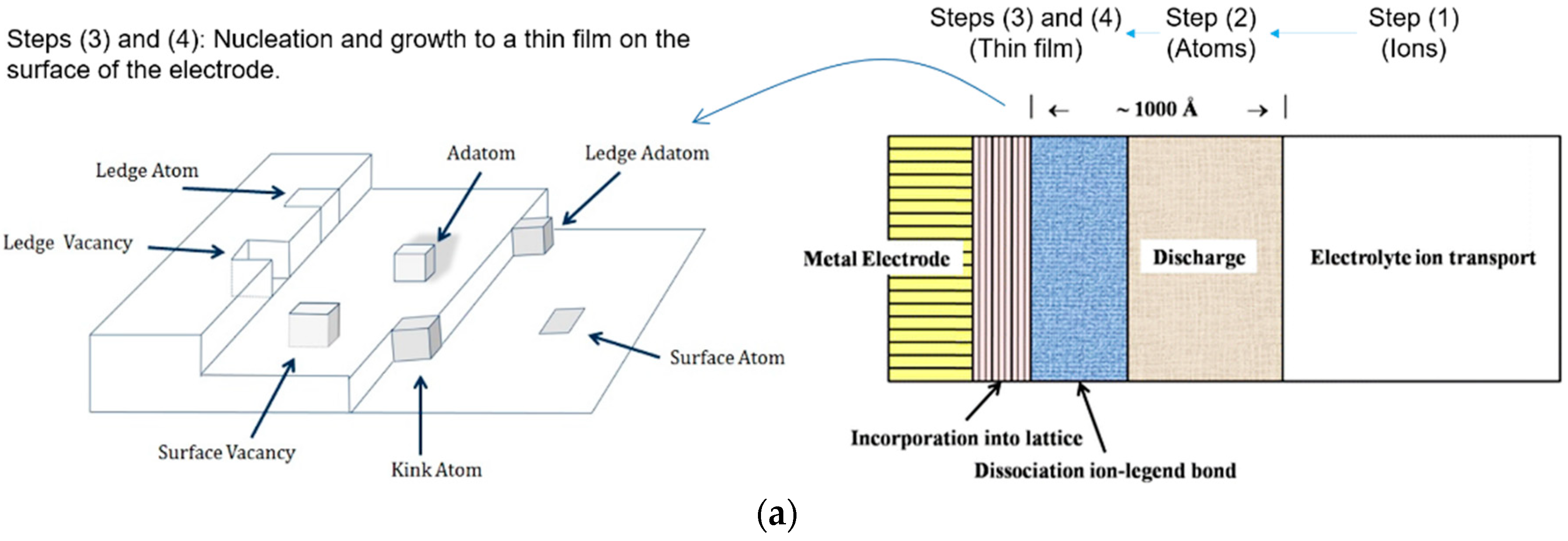
Electrodeposition typically involves four steps as schematically represented in Figure 2a: (1) Cations in the electrolyte are driven by the electric field and transport toward the cathode; (2) the cations enter the discharge region, which is within about 1–1000 Å from the cathode surface and where the cations receive electrons and turn to atoms; (3) the atoms diffuse to the cathode and then attach onto the cathode surface at energetically favorable sites and (4) the atoms aggregate and/or react to each other to form nuclei of an element, an alloy or a compound; the nuclei grow to grains and eventually result in the formation of a film on the surface of the cathode [27,28,29,30]. As a consequence of such a transport–adsorption–nucleation growth process, the grain size, morphology (i.e., microstructure), crystal structure and quality (e.g., the density and homogeneity) of films produced with an electrodeposition method are related to multiple factors, which primarily include:
  • The recipe, concentration and viscosity of the electrolyte,
  • The chemical environment of the electrolyte (e.g., the pH value),
  • Complexing agent added in the electrolyte,
  • Temperature during the deposition,
  • The voltage and current applied to the deposition bath and,
  • The condition of the substrate (at the cathode; e.g., the conductivity and surface roughness), which can affect the mass transfer of cations and the kinetics of the reaction at the cathode surface, either individually or jointly [31].
The mechanism of electrodeposition can also be better understood with the electrical double layer (EDL) model [32], as shown in Figure 2b. According to the EDL model, when a voltage is added to the deposition bath through the electrodes, i.e., anode and cathode, the cathode will be charged with the negative charges (i.e., electrons). This will result in the formation of a double layer at the interface between the cathode and electrolyte due to the electrostatic attraction of the negative charges in the cathode to the cations in the electrolyte. It has been found that, in a certain region, the electric potential on the electrolyte side decreases linearly as the distance from the cathode surface increases; such a region or zone has been named as the Helmholtz layer. As the distance increases further, the potential decreases exponentially—this zone is called the Gouy layer or diffusion layer. The electrodeposition primarily occurs in the Helmholtz layer, where the cations are attracted strongly to adsorb onto the cathode and reduced to neutral atoms or further react to each other to form an alloy or compound at the molecular level, eventually resulting in the formation of a thin film. The thickness of the Helmholtz layer can be thought of as the total length of the incorporation region, dissociation region and discharge region in the model shown in Figure 2a.

2.2. Two-Electrode and Three-Electrode Configurations

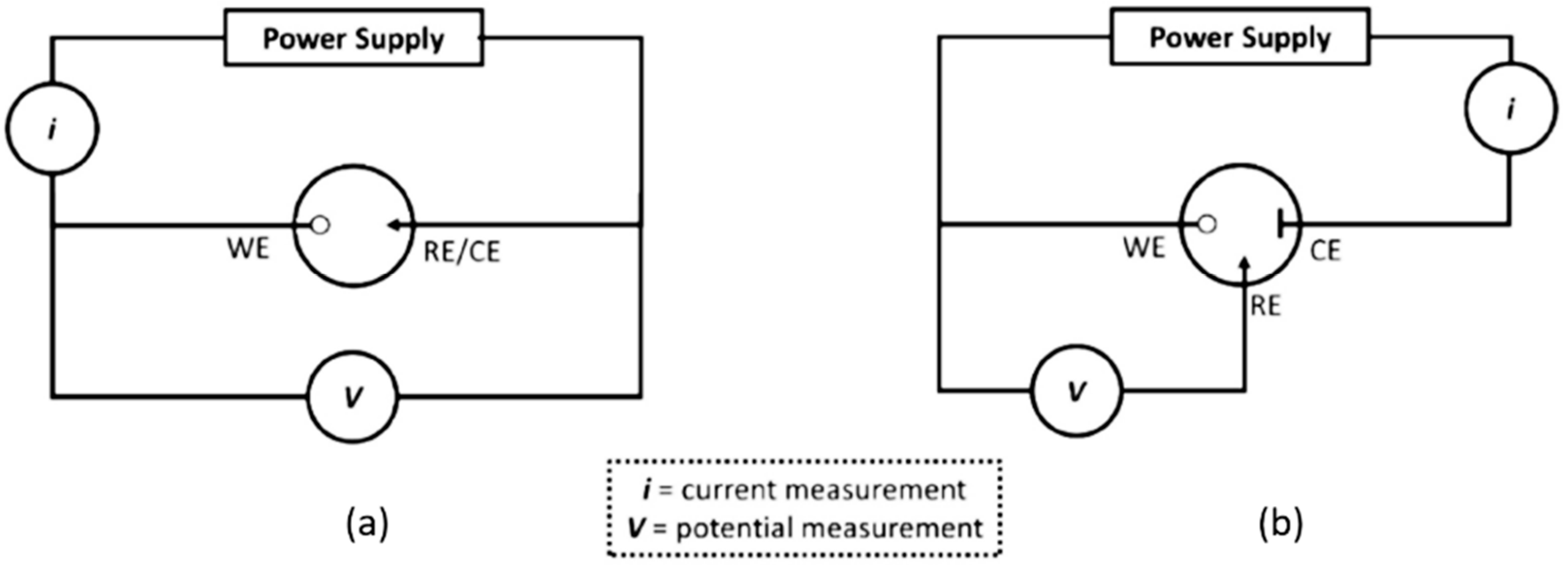
Electrodeposition can be performed with a two-electrode configuration or a three-electrode configuration as shown in Figure 3 [33]. A two-electrode configuration system consists of an anode and a cathode, which are connected to the positive electrode and negative electrode of the power supply, respectively (Figure 2a), causing an electric field pointing from the anode to the cathode through the electrolyte. A two-electrode configuration is simple. However, it suffers from a floating potential problem, i.e., the potentials of the electrodes may change during the deposition since none of the electrode potentials are fixed. Therefore, a two-electrode configuration system is only applicable for the deposition that operates under a constant current. A three-electrode configuration system that consists of a working electrode (WE), a counter electrode (CE) and a referent electrode (RE; Figure 3b) may greatly solve the floating potential problem in the two-electrode system and has been widely adopted in electrochemical analyses or the electrodeposition fabrication. A three-electrode configuration is advantageous in the use of a reference electrode to provide a stable potential, and the potential at the working electrode can therefore be controlled accurately and maintain at a constant value. This greatly benefits the electrochemical reactions that need to know the exact potential or occur at a certain potential. The common reference electrodes are a standard hydrogen electrode (SHE) (H2/H+) (E = 0 V), calomel (Hg/Hg2Cl2) electrode (E = 0.241 V vs. SHE in the saturated electrolyte solution at 25 °C), silver/silver chloride (Ag/Ag/Cl) electrode (E = 0.197 V vs. SHE), silver/silver sulfate (Ag/Ag2SO4) electrode (E = 0.68 V vs. SHE) and copper/copper(II) sulfate (Cu/CuSO4) electrode (E = 0.314 V vs. SHE). A three-electrode system can be converted to a two-electrode system by, as shown in Figure 3a, using the working electrode as the cathode and connecting the counter electrode (CE) together with the reference electrode (RE) as the anode.

2.3. Potentiostatic and Galvanostatic Modes

Electrodeposition can be performed in a potentiostatic mode or a galvanostatic mode. In two-electrode systems, the potentiostatic mode means a constant voltage is applied to the two electrodes. As a result, the potential difference between the two electrodes keeps constant, disregarding changes in the load or the resistance of the electrolyte. Rather than controlling the voltage, the galvanostatic mode controls the current flowing through the two electrodes and keeps the current constant. In three-electrode systems (Figure 3b), the potentiostatic mode means that the potential of the working electrode (WE) against the counter electrode (CE) is accurately controlled so that the potential difference between the working electrode (WE) and the reference electrode (RE) is well defined. The galvanostatic mode means the current flowing between the WE and the CE is under control, and the potential difference between the WE and RE is monitored. Galvanostatic deposition can be useful in applications where no control over morphology is necessary. The potentiostatic deposition technique, however, was mainly used to investigate the mechanisms of deposition and morphology formation [34]. The deposition of chalcogenide films for the photovoltaic device applications has been predominantly adopting the potentiostatic mode in view of the need of a morphology control for the films and also for the reason that the potentiostatic mode is more suitable for depositing multiple elements simultaneously, i.e., the so-called co-deposition that will be introduced in the following sections.

2.4. The Deposition Potential

In the simplest case when a single metal film is to be deposited, the deposition potential, i.e., the electrode potential or the operating potential, can be estimated through the reduction potential of the metal ions. The latter, which is also called the equilibrium potential between the metal and the solution of its ions, can be given by the Nernst equation as follows [35]:
E = E 0 + R T n F ln a
where, E is the reduction potential, E0 the standard reduction potential for the reaction M n + + n e M 0 versus the standard hydrogen electrode (SHE), R the gas constant (8.3143 J/k/mol), T the absolute temperature (K), n the valence change or the valence number of the metal element, F the Faraday constant and a the activity of the metal ion, which can approximately use the concentration of the metal ion in the electrolyte. To make the deposition happen, the electrode potential (i.e., the potential of the cathode versus the reference electrode) is required to be more negative than the reduction potential (i.e., the equilibrium potential). The difference between the electrode potential and the reduction potential is called the overpotential. In the case of depositing multiple elements at one time (i.e., the case of co-deposition), the electrode potential must be chosen to make sure that it is more negative than the most negative one among the potentials needed for the deposition of all elements.
Though the deposition potential can be estimated through the reduction potential, in practice, the deposition involves a complicated process and the needed potential is related to more factors than those in Equation (3). These may arise from the electrolyte, for example, the viscosity and the pH value of the electrolyte. It may also be caused by the conditions of electrodes such as the conductivity and the interface status between the electrode and electrolyte. In addition, the configuration of the deposition bath including the arrangement of the electrodes and the distance(s) between them may also have an impact on the practically needed deposition potential. Therefore, cyclic voltammetry (CV), a powerful experimental technique that can investigate the reduction and oxidation processes in an electrochemical system, has been commonly used to determine the reduction potential(s) of ions in an electrolyte [36].

3. Electrodeposition of Chalcogenide Films

3.1. Cadmium Chalcogenides

Cadmium chalcogenide compounds such as cadmium sulfide (CdS), cadmium selenide (CdSe) and cadmium telluride (CdTe) have been extensively used in solar cells. Electrodeposition is one of important and popular techniques for the fabrication of the films thereof.

3.1.1. CdS

Cadmium sulfide (CdS), which features a relatively narrow direct band gap (2.4 eV) and the large absorption coefficient (4 × 104 cm−1), is one of the most commonly used n-type semiconductors in photovoltaic devices [37]. CdS can be produced via electrodeposition in an acidic aqueous solution containing Cd2+ and sodium thiosulfate (Na2S2O3). The reactions can be described as follows [38]:
Na2S2O3 + H2O → S2O32− + Na2O + 2H+
Cd2+ + S2O32− + 2e → CdS + SO32−
Lade et al. studied the electrodeposition fabrication of CdS with a solution containing 0.5 M Na2S2O3 as the sulphur source, 0.05 M CdSO4 as the cadmium source and 0.1 M ethylenediaminetetraacetic acid (EDTA) as a complexing agent [39]. It was found that the deposition potential was affected by both the temperature of deposition and the pH value of the electrolyte. With increasing the temperature of deposition, the potential became more positive, and with increasing the pH value of the electrolyte, the potential became more negative. Therefore, in order to achieve stoichiometric CdS, the deposition temperature and the pH value of the electrolyte should be well balanced. It was also found that the films deposited at the temperatures below 70 °C presented a mixed phase of cubic CdS and hexagonal CdS, while those deposited above 70 °C showed a pure hexagonal phase. The crystallinity of the as-deposited films could be greatly improved by annealing the films at 200 °C. Echendu et al. found that the mixed phase always formed in the as-deposited films, even though the films were deposited at 80 °C [40]. However, it was observed that, after a heat treatment at 400 °C, all films deposited at different potentials turned to a pure hexagonal phase. The difference between Lade and Echendu’s work is that the latter has no a complexing agent used in the electrolyte.
Na2S2O3 is the most widely used S source for CdS electrodeposition. However, the drawback with this reagent is that sodium may dope CdS and cause a decrease in the electrical conductivity of the CdS film. This problem can be solved by employing ammonium thiosulphate ((NH4)2S2O3) as the S source. Alam et al. deposited an n-type CdS film with an electrolyte containing cadmium acetate and ammonium thiosulphate [41]. They found that the deposition resulted in uniform crystalline CdS films with the grain size in the range of 200–300 nm (Figure 4) in the case of the pH value of the solution being about 3 and the temperature being 85 °C.
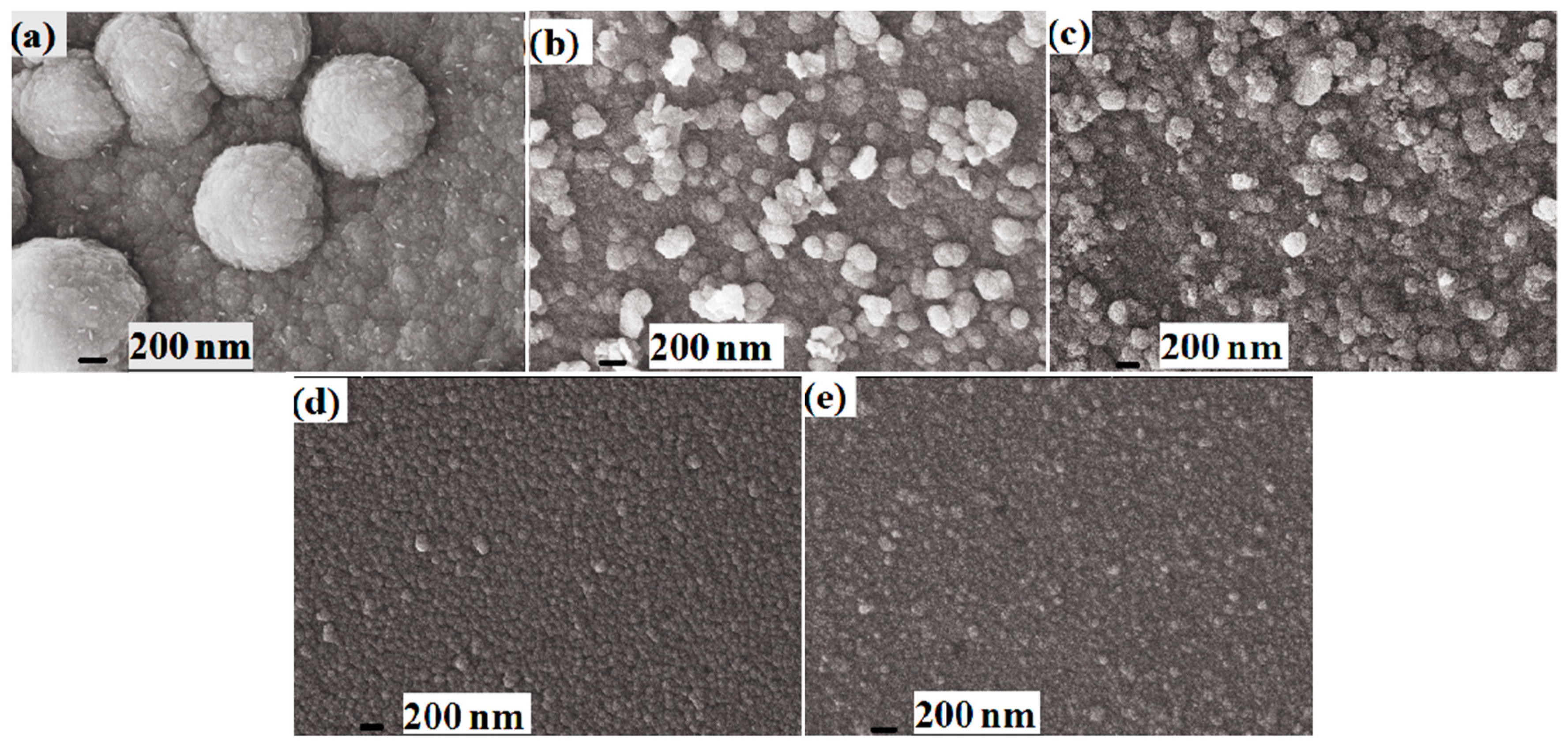
Altiokka et al. deposited CdS films when the pH value of the electrolyte varies [38]. They confirmed that the pH value of the electrolyte has an important impact on the morphology of the deposited film. They found that the electrolyte with a pH value below 3 caused S2O32− to decompose, resulting in the formation of a high concentration of S2− ions in the electrolyte. The S2− compounded with Cd2+, leading to the formation of CdS clusters (Figure 5a–c). The following reactions describe the decomposition of S2O32− and the generation of S2− ions:
S2O32− → S + SO32−
S(s) + 2e → S(aq)2−
When the pH was about 4–5, the concentration of S2− in the electrolyte was low. As a result, no clusters formed and the film presented a smooth surface (Figure 5d,e).
There have been some efforts made to improve the quality of electrodeposited CdS film by reducing the defects or increasing the crystallinity. The basic idea is to elevate the temperature during the electrodeposition through using ionic liquids or non-aqueous solvents, such as dimethyl sulfoxide (DMSO), dimethyl formamide (DMF), diethylene glycol (DEG) and ethylene glycol (EG) [42,43,44]. Macfarlane et al. used a methyltributylphosphonium (P1,4,4,4) tosylate ionic liquid for the electrodeposition fabrication of CdS. The deposition was performed at 130–150 °C, resulting in the formation of crack-free films of CdS well adhering on the FTO coated glass substrate. The films are polycrystalline and the atomic ratio of cadmium to sulfur was found to be nearly stoichiometric [45]. However, CdS clusters were observed in the films, due likely to the decomposition of S2O32− that gives rise to a high concentration of S2− in the electrolyte. Lade et al. deposited CdS thin films with an electrolyte containing 0.5 M Na2S2O3, 0.05 M CdSO4 and 0.01 M EDTA dissolved in ethylene glycol [44]. The deposition was conducted at 90–140 °C. The films were polycrystalline and all presented a pure hexagonal phase. It has been also observed that the deposition potential became more positive with increasing the temperature, and 90 °C seemed to be an optimized temperature that can result in uniform and crack-free films.

3.1.2. CdSe

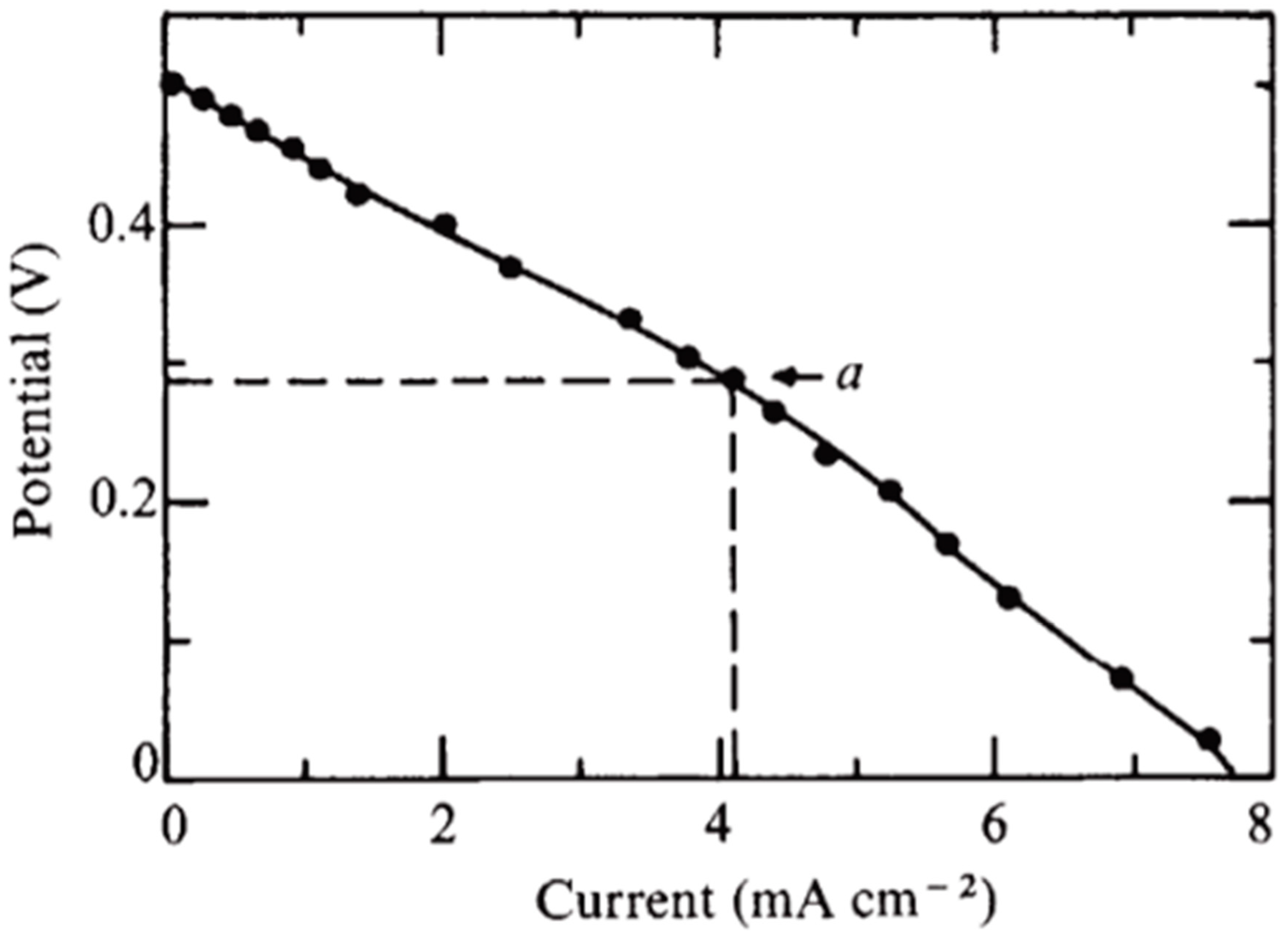
Hodes et al. first reported the electrodeposition fabrication of polycrystalline CdSe on a titanium substrate and the use of the CdSe film for a photoelectrochemical cell in 1976 [46]. The deposition was performed in an acidic aqueous solution of CdSO4 and SeO2. Shown in Figure 6 is the photoelectrochemical response (i.e., the current–potential curve) of the cell that used the deposited CdSe film as the photo cathode and an active carbon as the counter electrode. The electrolyte was 1 M S2−/S, and the measurement was carried out under AM1 sunlight. The cell achieved 450–560 mV open-circuit voltages and 7–10 mA·cm−2 short-circuit currents.
The process of the electrodeposition of CdSe in an acidic solution containing SeO2 and a cadmium salt can be described with the following equations [47,48,49]:
SeO2 + H2O → H2SeO3
H2SeO3 + 6H+ + 6e → H2Se + 3H2O (at the cathode)
Cd2+ + H2Se → CdSe + 2H+ (at the cathode)
where, the deposition potentials for Cd2+ + 2e → Cd and Se2− − 2e → Se are −0.403 V and +0.74 V, respectively. To this method, Kazacos et al. found that elemental Se was mixed in the product and proposed that the elemental Se was formed through the following reaction [47]:
2H2Se + H2SeO3 → 3Se + 3H2O
It has been reported that the use of complexing agents, for example, ethylenediaminetetraacetic acid (EDTA) or nitrilotriacetate (NTA), in the electrolyte is effective in removing elemental Se [47,50]. Annealing at low temperatures to make Se evaporated is another way to get rid of excess Se from the film [51].
CdSe can also been deposited in an alkaline solution [52]. The deposition takes place in an electrolyte containing cadmium-ethylenediaminetetraacetic acid, EDTA complex and selenosulfate through the following reaction [27]:
SeSO32− + 2e → Se2− + SO32−
(NH4)2Cd(EDTA) + (NH4)2SeSO3 + 2e → CdSe + (NH4)2(EDTA)2− + (NH4)2SO3
Kariper et al. reported the electrodeposition of CdSe in an electrolyte containing KOH with the pH greater than 10 [53]. The formation of CdSe was based on Cd2+ obtained from a cadmium salt and Se2− achieved by reducing elemental Se with LiAlH4. It has been found that CdSe films deposited in an alkaline solution are usually amorphous in nature (actually, this was also fairly often found in the films deposited in an acidic solution [54]). A post annealing treatment (e.g., at 300 °C) under a nitrogen atmosphere may significantly improve the crystallinity of the films [55]. In addition to promoting the crystallinity, post heat treatment may also cause a dramatic decrease in the band gap of the material. Chowdhury et al. observed that annealing electrochemically deposited CdSe film at 350 °C for 30 min may grow the grains to 300–750 nm and decrease the band gap from 2.1 eV for the as-deposited film to 1.8 eV for the annealed film [56].
In most cases, CdSe produced with an electrodeposition method is an n-type semiconductor [47,52,56,57,58]. The achievement of p-type CdSe is still challenging so far due to the self-compensation effect in the material. Ohtsuka et al. reported that p-type CdSe could be achieved by molecular beam epitaxy using a nitrogen plasma source [59,60]. However, there is generally a lack of facile methods for producing p-type CdSe.

3.1.3. CdTe

CdTe, a direct-band-gap material with a band gap of 1.54 eV, is another important cadmium chalcogenide than has been widely used for photovoltaic devices. In most of the reports, the electrodeposition fabrication of CdTe was conducted at a constant potential using an aqueous electrolyte with an acidic medium [61,62,63]. The following are the reactions occurring at the cathode where the CdTe is deposited [62,64,65]:
Cd2+ + 2e → Cd (E0 = −0.403 V vs. SHE)
HTeO2+ + 3H+ + 4e → Te + 2H2O (E0 = +0.551 V vs. SHE)
Cd + Te → CdTe (ΔG0 = −106.7 kJ/mol)
where, E0 is the standard deposition potential, and ΔG0 is the Gibbs free energy of formation. According to the deposition potentials for Cd and Te, it can be seen that more negative potentials may result in an increase in the Cd concentration and more positive potentials may lead to the formation of a Te-rich CdTe film [62]. It has been reported that Cd-rich CdTe results in n-type conduction and Te-rich CdTe results in p-type conduction [66,67,68]. Therefore, for the electrodeposition fabrication of CdTe, the conduction type of the film can be tuned by adjusting the deposition potential around the potential of perfect stoichiometry (PPS). Takahashi et al. studied the electrodeposition fabrication of n-CdTe and p-CdTe, and achieved n-CdTe when the potentials are between −0.60 and −0.45 V (versus Ag/AgCl) and achieved p-CdTe when the potentials are more positive, between −0.35 and −0.3 V [69].
Besides the deposition potential, the performance of the film is also related to other factors, such as the concentration and pH value of the electrolyte, stirring speed, the temperature of operation, and the temperature for post heat treatment. It seems that a low concentration of telluric ions (Te4+) and the pH around 2 for the electrolyte are suitable conditions for the formation of CdTe, which was reported a preferred orientation along the (111) plane [70]. The annealing temperature also plays a vital role in affecting the quality and properties of the deposited film [71,72]. It was found that the crystallinity of CdTe films deposited at optimized conditions can be greatly improved after being annealed at the temperatures ranging from 200 to 450 °C [73,74].
Basol et al. fabricated a solar cell constructed with CdS and CdTe — both films were produced via electrodeposition. Figure 7 shows the configuration of the solar cell [75]. The fabrication involved the deposition of a thin layer of CdS film onto a fluorine doped tin oxide (FTO) glass substrate first, followed by the deposition of a CdTe layer. The films were then annealed at 400 °C to enable the formation of a heterojunction between the CdS and CdTe. At last, a gold film was deposited on the CdTe as the back contact. The solar cell achieved a solar-to-power conversion efficiency as high as 9.35% [76]. Such an efficiency is very impressive. It makes the electrodeposition a competitive technique for the CdTe solar cell fabrication when considering the significantly lower cost of electrodeposition than the vacuum methods, though the latter demonstrated higher efficiencies, around 13% [77].
CdTe can also be deposited in alkaline solutions [78,79]. Zhang et al. deposited highly crystallized and well (111)-oriented CdTe with an alkaline solution containing nitrilotriacetic acid (NTA) and tetramethylammonium hydroxide (TMAH) [79]. It was explained that NTA (at the NTA to Cd ratio of 14:1) acted as a complexing agent that improved the crystallinity of the deposited CdTe, and TMAH was adopted to prevent alkaline metal ions from entering the CdTe film. The mechanism of the CdTe deposition was given as follows:
TeO32− + 3H2O + 4e → Te + 6OH
Cd(NTA)n2+ → Cd2+ + nNTA
Te + Cd2+ + 2e → CdTe

3.2. Zinc Chalcogenides

Zinc chalcogenides such as ZnS, ZnSe and ZnTe with a relatively wide energy band gap have been widely used as the active layer (which meanwhile acts as a buffer layer) or window layer materials in photovoltaic devices.

3.2.1. ZnS

ZnS is an inexpensive semiconductor with an energy band gap of 3.72 eV in the cubic phase and 3.77 eV in the hexagonal wurtzite phase. In thin film photovoltaic devices, ZnS has been majorly employed as an n-type material to form a p–n junction by pairing with a p-type material, for example, Cu(In,Ga)Se2 (CIGSe) [80] or Cu2ZnSnS4 (CZTS) [81,82]. ZnS can be electrochemically deposited with either an alkaline electrolyte or an acidic electrolyte. Mkawi et al. reported the use of an aqueous electrolyte containing zinc sulfate (ZnSO4), thiourea (CS(NH2)2) and ammonia (NH3) for the deposition of ZnS on ITO-coated glass substrate [82]. The pH value of the electrolyte was 10 and the deposition was carried out at 80 °C. It was explained that NH3 functioning as a complexing agent formed a complex with Zn and thus played a role in controlling the concentration of Zn2+ through the common ion effect. The involved reactions are shown in Equations (20) and (21):
ZnSO4 + 6NH3 → SO42− + Zn(NH3)62+
Zn(NH3)62+ → 6NH3 + Zn2+
The thiourea decomposed to S2− in the presence of OH via the reactions below, finally resulting in the formation of ZnS:
CS(NH2)2 + OH → SH + CH2N2 + H2O
SH + OH → S2− + H2O
Zn2+ + S2− → ZnS
In order to achieve stoichiometric ZnS, a sulfurization treatment of the as-deposited film under nitrogen at 500 °C was performed. The ZnS presented a cubic phase, an energy band gap of 3.72 eV, and the grain size of 44 nm. This is in agreement with the 3.70 eV energy band gap for the ZnS fabricated by Lokhande et al. with a NaOH and EDTA mediated alkaline electrolyte [83].
ZnS can also be deposited with an acidic solution. Zhu et al. succeeded in the fabrication of ZnS with an electrolyte of zinc chloride (ZnCl2), sodium thiosulphate (Na2S2O3·5H2O) and sodium citrate (Na3C6H5O7·2H2O) dissolved in deionized water, to which hydrochloric acid was added to adjust the pH value of the electrolyte [84]. It was found that uniform films of crystalline ZnS could be achieved when the pH value was in the range from 2.5 to 4.0. In the case of the pH value being below 2.5, S2O32− rapidly reduced to S2−, resulting in a rapid growth of ZnS with much lattice defects. Sodium citrate acted as a complexing agent to suppress the concentration of free Zn2+ ions in the electrolyte. The reactions leading to the formation of ZnS were proposed as follows:
S2O32− + 6H+ + 4e → 2S + 3H2O
S + 2e → S2−
Zn2+ + Na3C6H5O7 → [Zn(C6H5O7)] + 3Na+
[Zn(C6H5O7)] → Zn2+ + C6H5O73−
Zn2+ + S2− → ZnS
Matsuda et al. studied the electrodeposition of ZnS [85]. They found that a combined use of boric acid to control the pH of the electrolyte and a mixture of citrate acid and malonic acid as the complexing agent could best avoid the formation of ZnO and result in ZnS with high purity. They also reported that adding CuSO4 in the electrolyte could achieve Cu-doped ZnS with the energy band gap as narrow as 1.8–1.9 eV. Madugu et al. deposited ZnS with an aqueous electrolyte that consisted of ZnSO4, (NH4)2S2O3 and H2SO4 (added to adjust the pH value) using a two-electrode system. It was found that the conduction type (i.e., p-type and n-type) of ZnS could be tuned by simply varying the deposition potential [86]. As shown in Figure 8, in the potential window ranging from 1400 to 1500 mV, the as-deposited ZnS presented to be p-type when the cathodic potentials were lower than 1450 mV and to be n-type at the potentials above 1450 mV. The p-type conduction and n-type conduction were attributed to S richness and Zn richness in the composition, respectively. After a heat treatment at 350 °C for 15 min in air, all films that were previously n-type turned to p-type.
Regardless of the use of an alkaline or acidic electrolyte, in most of cases the as-deposited ZnS is either an amorphous structure or possesses a cubic phase [82,84,86]. Annealing at a temperature above 200 °C may promote the crystallization and enable the formation of a hexagonal phase of ZnS [87].

3.2.2. ZnSe

ZnSe, which exhibits an energy band gap of 2.8 eV, is another important material for photovoltaic devices. ZnSe has been particularly used for Cu(In,Ga)Se2 (CIGS) solar cells in view of the small lattice mismatch between ZnSe (a = 0.5667 nm) and CIGS (a = 0.56 − 0.58 nm) [88,89,90]. The electrodeposition of ZnSe is usually performed with an acidic electrolyte when the pH value is at 2–2.5. Selenous acid (H2SeO3) has been the mostly used chemical for the Se source. H2SeO3 can be prepared by dissolving SeO2 in water [91,92]. Since H2SeO3 may oxidize readily, the deposition is usually carried out under an inert atmosphere. Natarajan et al. [93] and Kowalik et al. [94] produced ZnSe with an electrolyte of H2SeO3 and ZnSO4, which used sulfuric acid (H2SO4) to adjust the pH value. The formation of ZnSe was based on the reactions as follows:
H2SeO3 + 4H+ + 4e → Se + 3H2O
Zn2+ + Se + 2e → ZnSe
The concentration of the selenous acid might influence both the deposition rate and the crystal structure of the ZnSe. The higher concentration accelerated the deposition and benefited the formation of crystalline ZnSe (in a cubic phase). The crystal structure of the deposited ZnSe was also affected by the deposition temperature. It was found that the films deposited at 25 °C were almost amorphous, and higher temperatures (e.g., 75 °C) resulted in better crystallinity. A post heat treatment could further improve the crystallinity of the films and increase the orientation of the crystallites [95].
Note that the electrodeposited ZnSe may present an n-type conduction characteristic or a p-type conductivity, depending on the recipe of the electrolyte and the deposition parameters, which likely cause different dominant defects in ZnSe but the exact relationships are still unclear [96]. Manzoli et al. reported that ZnSe deposited in an electrolyte containing SeO2, ZnSO4 and sulfuric acid was n-type, and it was p-type when ZnSe was doped with N by including (NH4)2SO4 in the electrolyte [97]. However, Gromboni et al. used a similar electrolyte but found the undoped ZnSe was p-type [98]. Samantilleke et al. also found that the deposited ZnSe was p-type, and found n-type ZnSe could be achieved by doping ZnSe with Ga through including Ga2(SO4)3 in the electrolyte [99].

3.2.3. ZnTe

ZnTe is a semiconductor with a low electron affinity (3.53 eV) and high electro-optic coefficient. ZnTe usually presents a p-type conduction characteristic with the mobility as high as 100 cm2V−1s−1, and has been extensively studied for the applications in photovoltaic devices, in particular in CdTe/CdS heterojunction solar cells, where ZnTe is used as the back contact material for CdTe [100,101]. It is worth pointing out that, as for the fabrication of CdTe/CdS heterojunction solar cells, electrodeposition has been considered as a preferred method in view of its capability in the creation of continuous and very thin (<100 nm) ZnTe films—it is however difficult to be achieved with vacuum deposition [102].
The electrodeposition of ZnTe can be achieved with an aqueous electrolyte consisting of ZnSO4, TeO2 and H2SO4, where H2SO4 is employed to adjust the pH value of the electrolyte [103]. It was proposed that TeO2 first dissolved in water, resulting in the formation of HTeO2+; ZnTe was then deposited at the cathode (i.e., the working electrode) through the following reactions:
HTeO2+ + 4e + 3H+ → Te + 2H2O
Zn2+ + Te + 2e → ZnTe
Mahalingam et al. reported that a smooth and dense ZnTe film with a cubic phase and the stoichiometric composition could be achieved at the deposition potential between −0.95 and −1.25 V vs. SCE, the pH value of 3.5, and the deposition temperature of 90 °C [103]. The energy band gap of the deposited film was 2.26 eV. Skhouni et al. deposited ZnTe through dissolving TeCl4 in HCl to form HTe; the HTe further compounded with Zn2+ (from ZnCl2), leading to the formation of ZnTe. The reaction is a proposed as follows [104]:
HTe + Zn2+ + H2O → ZnTe + H3O+
The deposition was carried out at 80 °C when the pH value of the electrolyte was 3.60–3.78 and the deposition potential was −0.85 V vs. Ag/AgCl. The film was then annealed at 350 °C in vacuum for 20 min, resulting in the formation of a p-type ZnTe film possessing a nearly stoichiometric composition (Zn:Te = 1:0.99), a cubic phase and good crystallinity. Bouroushian et al. found that, by adding citric acid and sodium citrate to the electrolyte as the complexing agents, extremely smooth and uniform ZnTe films could be produced [105].
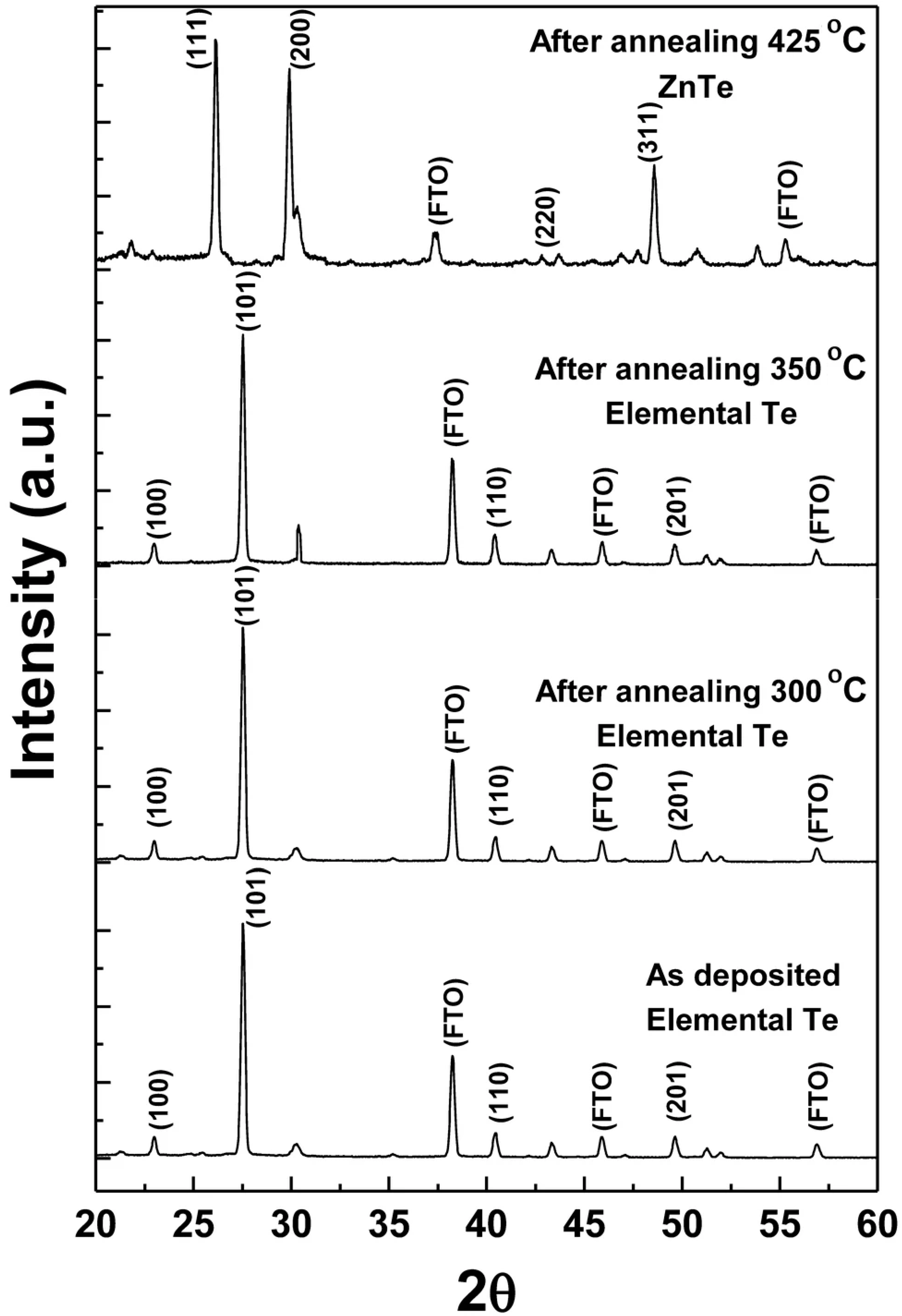
Besides in acidic aqueous electrolytes, the deposition of ZnTe can also be performed in organic solvent or ionic liquid based electrolytes. Hossain et al. reported the fabrication of ZnTe films with an electrolyte consisting of ZnCl2, TeCl4 and KI dissolved in ethylene glycol (EG) [106]. It was found that, as indicated by the X-ray diffraction (XRD) spectra shown in Figure 9, well-crystallized ZnTe with a pure cubic phase could be achieved by annealing the as-deposited films at 425 °C. The XRD else revealed that the annealing also functioned to remove elemental Te that existed in the as-deposited film. Catrangiu et al. deposited ZnTe with an ionic liquid electrolyte that used ethaline (prepared by reacting choline chloride with ethylene) as the solvent [107]. The deposition was conducted at 60 °C. The resulting ZnTe films presented a crystalline structure with mixed cubic and hexagonal phases.
ZnTe has been used in CdTe/CdS solar cells primarily as the back contact material for CdTe. Its role is to reduce the interface states between the metal electrode and CdTe, and thus lower the charge recombination loss when electrons inject from the metal electrode to the CdTe. Jun et al. deposited p-type ZnTe through adding a complexing agent containing Cu2+ in the electrolyte to achieve copper doping. They reported that the use of the copper-doped ZnTe caused the efficiency of a CdTe/CdS solar cell to increase from 3.4% to 7.1% [100].

3.3. Copper Chalcogenides

Copper chalcogenides are a family of copper-based semiconductors. Almost all of the copper chalcogenides are p-type, possess a direct, narrow band gap (<2 eV) and have a large light absorption coefficient (104–105 cm−1) and low thermal conductivity. Copper chalcogenides such as copper selenide (CuxSe), copper telluride (CuxTe), copper indium selenide (CIS), copper indium telluride (CIT) and copper zinc tin sulfide (CZTS) have been the highly frequently used semiconductor compounds for photovoltaic devices. Copper chalcogenides are also important materials to light emitting diodes (LEDs) and thermoelectric (TE) devices [108].

3.3.1. Copper Selenides

Lippkow et al. studied the electrodeposition of copper selenide with an acidic aqueous electrolyte containing CuSO4, H2SeO3 and H2SO4 at pH = 1.4 [109]. It was found that the resulting product was polycrystalline and was a mixture of Cu2Se and Cu3Se2, which formed through the following reactions:
Cu2+ + SeO32− + 6H+ + 6e → CuSe + 3H2O
Cu2+ + CuSe = 2e → Cu2Se
2Cu2+ + SeO32− + 6H+ + 8e → Cu2Se + 3H2O
3Cu2+ + 2SeO32− + 12H+ + 14e → Cu3Se2 + 6H2O
It was pointed out that an optimal ratio for [Cu2+]/[SeO32−] is 2, which might minimize the formation of elemental Cu and Se. The adoption of a high deposition temperature, e.g., 80 °C, was prone to the formation of Cu2Se. A heat treatment of the as-deposited films at a temperature greater than 150 °C might convert all Cu3Se2 to Cu2Se. Dergacheva et al. found a similar optimal ration for Cu(II) to Se(IV) while Na2SeO3 was used for the electrolyte, and also observed that annealing the deposited films (at 300 °C) might promote the conversion of Cu3Se2 to Cu2Se [110].
Grozdanov reported the use of an alkaline electrolyte to deposit Cu2Se [111]. The electrolyte contained CuSO4, sodium selenosulfate (Na2SeSO3) and ammonia, and the pH was about 10–10.5. The deposition was conducted at 40–45 °C. The overall reaction that resulted in the formation of Cu2Se was proposed as follows:
2[Cu(NH3)4]2+ + SeSO32− + 2OH → Cu2Se + 8NH3 + SO42− + H2O

3.3.2. Copper Tellurides

The reactions for the deposition of copper tellurides are very similar to those for the deposition of copper selenides, except the use of H2TeO3 or TeO2 dissolved in water as the Te source. In the case of the electrolyte being an acidic solution, the deposition is based on the reaction between Cu2+ and TeO32−, resulting in the formation of stoichiometric CuTe or non-stoichiometric CuxTe (1< x < 2) [112,113].
xCu2+ + TeO32− + 6H+ + 8e → CuxTe + 3H2O
The composition of the deposited copper tellurides is very sensitive to the recipe of the electrolyte, including the reagents used as the Cu and Se sources and the pH value of the electrolyte. It is also related to the deposition temperature and the applied deposition potential. The use of a complexing agent may also influence the composition of the deposited copper telluride significantly. Ghosh et al. found that the deposited copper telluride was Cu7Te4 when Na2EDTA was added in the electrolyte (pH = 2.0) as the complexing agent to control the reaction kinetics [114].
In the case of the electrolyte being a neutral aqueous solution, the Cu2+ may be reduced to Cu+, enabling the formation of Cu2Te. He et al. suggested the following reactions for the deposition of Cu2Te [112]:
2Cu2+ + 2e + 2OH → Cu2O + H2O
H2TeO3 + 4H+ + 4e → Te + 3H2O
Te + 2H+ + 2e → H2Te
Cu2O + H2Te → Cu2Te + H2O
Similar to ZnTe introduced Section 3.2.3, Cu2Te is also a p-type material that has been adopted in CdS/CdTe solar cells for the interfacial layer added between the metal electrode and CdTe to reduce the charge recombination [115,116].
There were also some reports that explored the use of ionic liquid electrolytes for the deposition of copper tellurides [117,118].

3.3.3. Copper Indium Selenides (CIS)

Copper indium selenides (CuInSe2) can be electrochemically deposited with an electrolyte containing CuSO4, In2SO4, citric acid and SeO2 at pH = 2.1 [119]. Guillemoles et al. suggested that the CuInSe2 was formed through the following reactions [120]:
Cu(II) + αSe(IV) + (2+4α)e → CuSeα
3Se(−II) + 2In(III) → In2Se3
In2Se3 + Cu2Se → 2CuInSe2
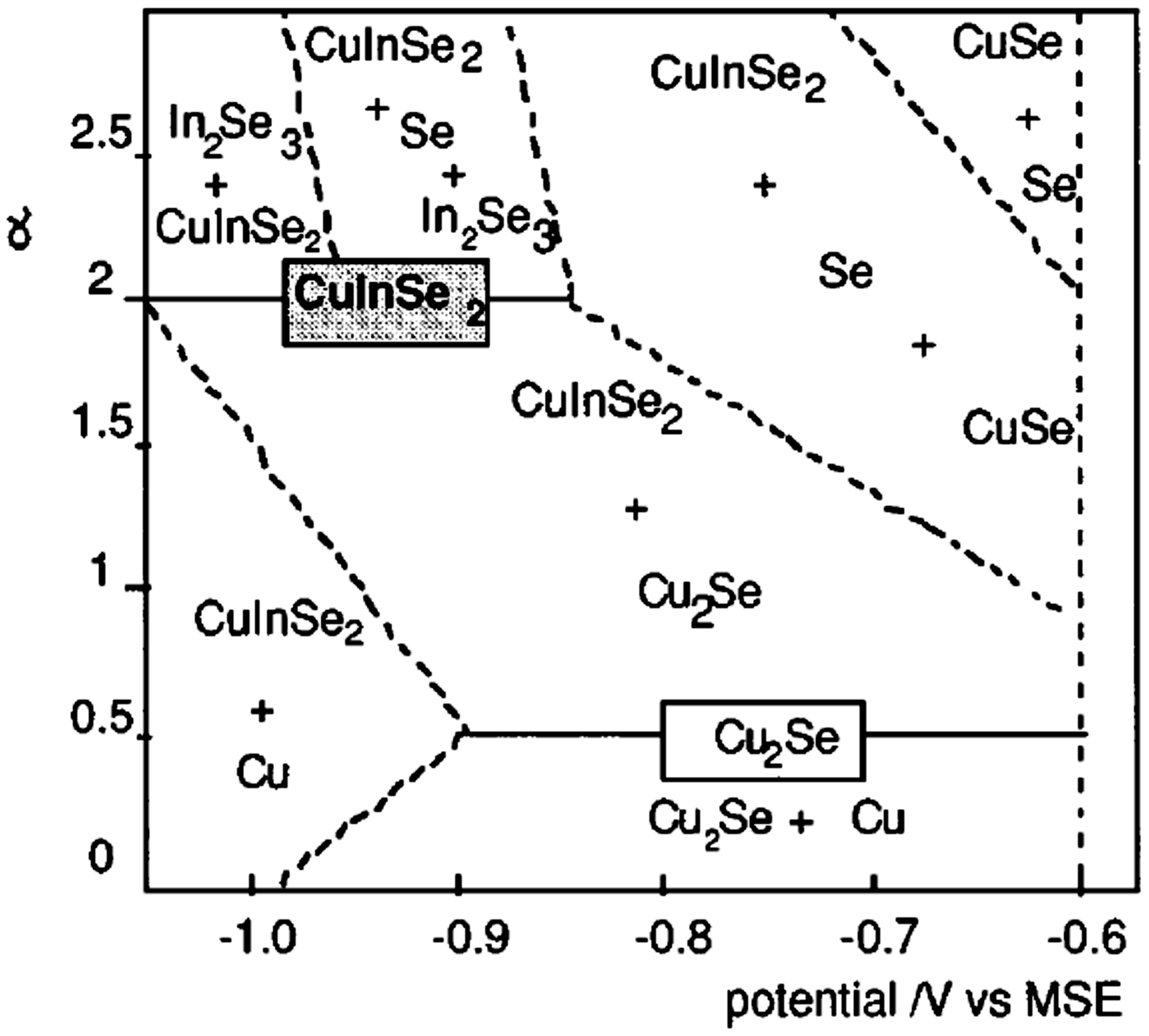
where, α is the ratio of the concentrations of Se(IV) and Cu(II) in the electrolyte, i.e., α = Jse/Jcu. Figure 10 is the zone diagram of the composition of the electrodeposited films as a function of the applied potential and α. It can be see that the optimal value of α for the formation of CuInSe2 is 2; in a given range of deposition potential, the film is copper rich when α < 2, and is indium rich when α > 2 [119]. It has been basically established that copper rich and indium rich results in p-type and n-type CuInSe2, respectively [121,122]. However, in the literature, one can also see an opposite relationship between the copper and indium richness and the p- and n-type conduction [123].
Chiang et al. achieved an efficiency as high as 6.46% with a solar cell constructed with co-electrodeposited CuInSe2. The CuInSe2 was fabricated on a Mo-coated glass substrate and was then deposited with a CdS film via chemical bath deposition (CBD) to form a p–n junction. The high efficiency was attributed to heating the electrolyte and substrate to 50 °C and 70 °C, respectively, during the electrodeposition, which led to the CuInSe2 with a smooth and defect-free surface that resulted in high quality to the interface between the CuInSe2 and CdS, while the one with the CuInSe2 produced without heating only received an efficiency of 0.49% [124]. Such a 6.46% efficiency is just slightly lower than the 6.6% efficiency reported by Dale et al. with electrodeposited CuInSe2 that however experienced a further selenization treatment [125]. Ulah et al. electrodeposited CuInSe2 on a fluorine-doped tin oxide (FTO) glass substrate instead of a Mo-coated glass substrate to form a solar cell with a configuration of FTO/CuInSe2/CdS/ZnO. The deposition was conducted at room temperature, and the CuInSe2 film was further selenized (at 500 °C for 40 min). The solar cell efficiency that they reported was 2.22% [121]. The low efficiency may arise from the destruction caused to the FTO film during the selenization. Londhe et al. explored CIS solar cells with an inverted structure, in which CdS was first deposited onto a FTO glass substrate, followed by the deposition of CuInSe2 and gold electrode, resulting in a solar cell configured as FTO/CdS/CuInSe2/Au [126]. The solar cell achieved an efficiency of 4.5%. Note that, in Londhe’s work, the CuInSe2 was also deposited at a high temperature (130 °C) but, differently, a further selenization treatment at 400 °C for 20 min was applied. The solar cell still presented a relatively high efficiency due likely to the CdS layer, which protected the FTO film to some extent during the selenization. The solar cell might have else benefited from the inverted structure that enables the light to be introduced from the FTO side and may therefore get more light harvested compared with the conventional case where the incident light is introduced from the metal electrode side. Fischer et al. studied the solar cell performance of CuInSe2 produced by depositing indium selenide and copper selenide successively and then selenizing at 550 °C for 30 min, and suggested that co-deposition (resulting in 6.6%) is more advantageous than the successive deposition method (5.5%) in terms of achieving a high solar-to-power conversion efficiency [123].

3.3.4. Copper Indium Tellurides (CIT)

The deposition of copper indium tellurides (CuInTe2) can be achieved through the reactions mentioned above for the copper indium selenides, except replacing the SeO2 with TeO2. Mahalingam et al. reported that 65 °C was an optimal temperature for the deposition, which resulted in CuInTe2 films with satisfactory crystallinity [127]. It was also found that the deposition potential had a significant impact on both the crystallinity and the composition of the deposited films. With an optimal deposition potential (at −0.9 V vs. SCE), well crystallized CuInTe2 with a nearly stoichiometric molar ratio, 1:1.03:1.67 for Cu:In:Te, was achieved. Lakhe et al. deposited CuInTe2 with a more acidic electrolyte (pH = 2) at a higher temperature (80 °C) [128]. They studied the influence of the deposition potential on the crystal structure when the potential varied in the range from −0.6 to −0.75 V (vs. Ag/AgCl reference electrode), and found that (1) the product included secondary phases such as In2O3 and In4Te3; (2) more negative potential might promote the formation of CuInTe2 and (3) pure-phase CuInTe2 was obtained on the films deposited at the potential of −0.75 V and then annealed at 400 °C for 15–20 min. Prasher et al. used an aqueous electrolyte containing CuCl2, InCl3, pre-reacted tellurium with HNO3 and acetonitrile [129]. The pH value of the electrolyte was 1.4 and the applied deposition potential was 0.35–0.4 V (vs. the Ag/AgCl electrode). They found that the resulting film was indium-rich CuInTe2 and emphasized that the adoption of stirring during the deposition could promote forming CuInTe2 with better stoichiometric composition and improved crystallinity.
Lakhe et al. studied the solar cell performance of electrodeposited CuInTe2 [128,130,131]. The CuInTe2 film was deposited on a FTO glass substrate on which a CdS layer was pre-produced via chemical bath deposition (CBD). The obtained CdS/CuInTe2 heterojunction was then annealed at 450 °C for 30 min (in air). The solar cell was configured as FTO/CdS/CuInTe2/Au, i.e., an inverted structure, in which electrons and holes diffuse to the FTO electrode and metal electrode, respectively. It was found that CuInTe2 deposited through the electrolyte with a pH value of 2 was copper rich, leading to a relatively high solar-to-power conversion efficiency, 4.13% [128], whereas CuInTe2 deposited with the electrolyte, which pH = 4, was however copper poor (or, indium rich) and, consequently, gave rise to somewhat low efficiencies ranging from 3.8% [130] to 4.01% [131].

3.3.5. CIGS

Copper indium gallium selenide (CIGS) is a quaternary compound composed of copper, indium, gallium and selenium with a formula of Cu(In,Ga)Se2 or CuInxGa(1−x)Se2. CIGS has a narrow energy band gap (1.0–1.7 eV) and an exceptionally high absorption coefficient of more than 105 /cm, and has been one of the major materials for polycrystalline thin film solar cells [132]. Figure 11 is a schematic drawing of the state-of-the-art structure of CIGS solar cells, in which CIGS is a p-type material and acts as the absorber layer. The CIGS solar cells typically use a Mo-coated glass as the substrate because of the satisfactory stability of Mo during the selenization. The CIGS film forms a p–n junction with an n-type CdS film; the latter is also known as the buffer layer of the solar cell. Above the CdS layer is usually a transparent layer of ZnO material fabricated to serve as the window layer of the solar cell and provide protection to the CdS layer. Solar cells with the CIGS material have demonstrated efficiencies over 20%. Industry widely employs vacuum deposition for the fabrication of CIGS films. However, due to the low cost and the compatibility with large-area fabrication, non-vacuum methods represented by the electrodeposition and nanoparticle ink-based screen-printing are earning increasing attention, though these methods face challenges in achieving high quality CIGS.
There are generally two methods to fabricate CIGS via electrodeposition: one-step co-deposition method and two-stage selenization method.
(1)
One-Step Co-Deposition Method
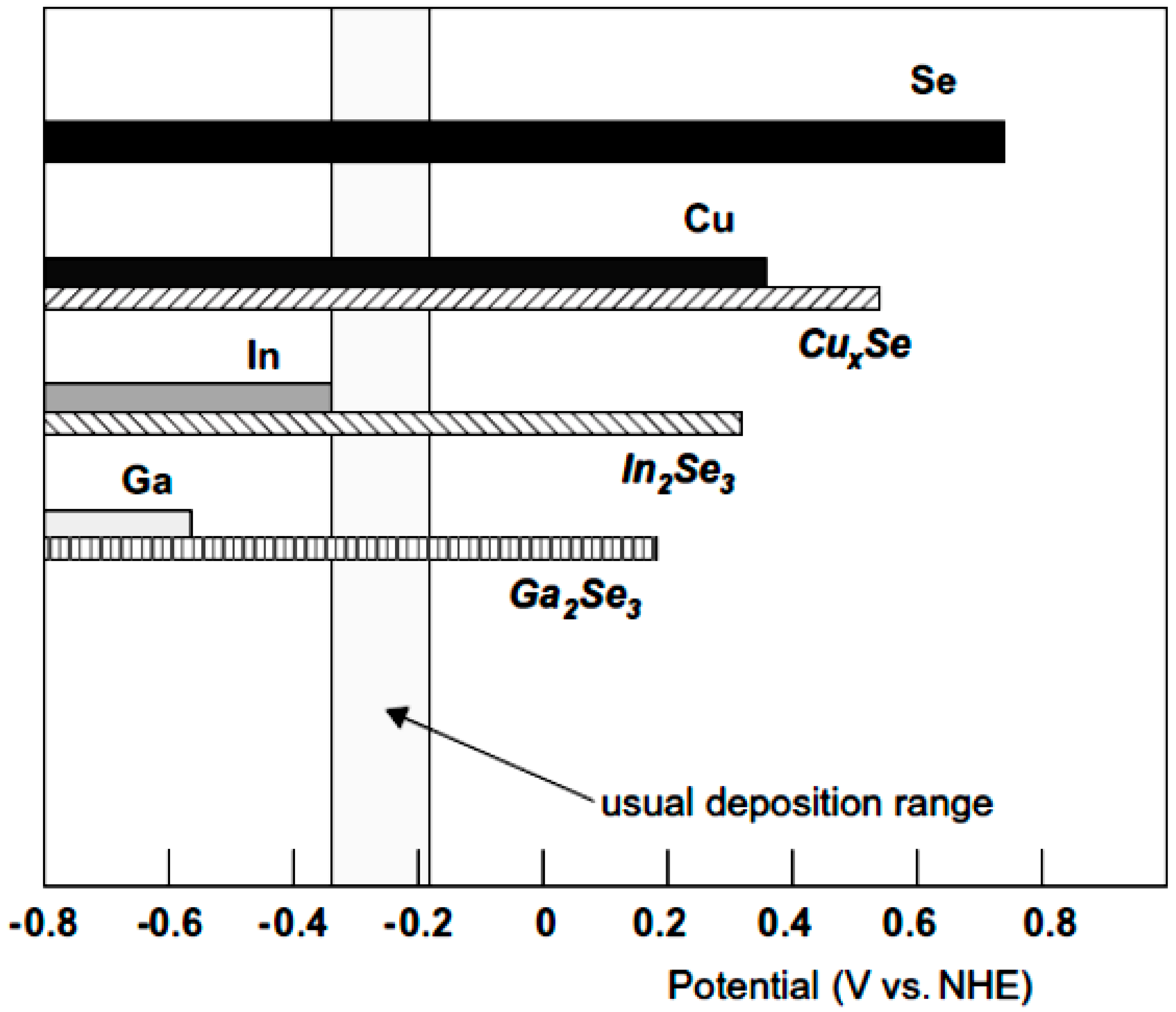
The one-step co-deposition method is similar to the methods used to deposit other binary or ternary chalcogenides as introduced above. The deposition uses an electrolyte that contains all reagents for Cu, In, Ga and Se, forming CIGS at the cathode via a number of electrochemical and chemical reactions. Since a wide distribution of the reduction potentials (Figure 12), +0.740, +0.342, −0.338 and −0.523 V vs. SHE for Se4+/Se, Cu2+/Cu, In3+/In and Ga3+/Ga, respectively, the one-step co-deposition is usually difficult in synthesizing stoichiometric CIGS [133]. In particular, Ga has a very negative (the most negative) reduction potential and therefore is difficult to be incorporated into the deposited film. This is in agreement with the experimental observation that the co-deposition is prone to yield CIGS with an obviously low content of Ga [132]. Such a scenario has motivated people to make further efforts to optimize the deposition parameters, for example, the pH and concentration of electrolyte, complexing agent used for the electrolyte, the deposition potential, and so forth, towards making the deposition potentials of all individual elements come close to each other. In practice, though the co-deposition method aims at one-step fabrication by including all sources of the elements in the electrolyte, a heat treatment of the as-deposited film (typically at 500–550 °C) to improve the crystallinity is usually still performed in an atmosphere that contains Se, in order to avoid the loss of Se from the film during the heat treatment.
Bhattacharya et al. studied the electrodeposition of CIGS with an aqueous electrolyte containing CuCl2, InCl3, GaCl3 and H2SeO3 at pH = 2–3 and a constant current density of 0.9 mA/cm2. They suggested that the electrodeposition of CIGS on the cathode is caused by the combination of electrochemical and chemical reactions as follows [134]:
Cu2+ + 2e → Cu(s)
In3+ + 3e → In(s)
Ga3+ + 3e → Ga(s)
H2SeO3 + 4H+ + 4e → Se + 3H2O
HSeO3 + 5H+ + 4e → Se + 3H2O
SeO32− + 6H+ + 4e → Se + 3H2O
Besides elemental Cu, In, Ga and Se involving in the deposition, Bhattacharya et al. also suggested that the deposition also included a direct deposition of selenide compounds such as Cu-Se, In2Se3, Ga2Se3 and CuInSe2 resulting from the reactions between the elements, for example, 2In3+ + 3Se + 6e → In2Se3. The deposited film was annealed in Se atmosphere at 550 °C for 30–45 min, leading to the formation of crystalline Cu0.94In1.04Ga0.07Se2. The solar cell constructed with the as-prepared CIGS delivered a decent solar-to-power conversion efficiency, 10.9%, though the nonstoichiometric composition arising from the low Ga content.
The low Ga content is due to the much negative deposition potential required for Ga3+/Ga. Long et al. reported that, compared to the case of an aqueous electrolyte, the use of ethanol as the solvent of the electrolyte might allow one to apply a more negative potential and accordingly increase the Ga content in the CIGS [135]. By using an electrolyte of CuCl2, InCl3, GaCl, H2SeO3 and LiCl dissolved in ethanol with the pH value adjusted to 1.9–2.2 with HCl, they deposited CIGS at the potential of −1.6 V vs. SCE. The film was then annealed at 550 °C for 30 min. It was found that the resulting film was only slightly Cu-poor and the ratio of [Ga] to [Ga+In] reached 0.25. The formation of CIGS was proposed as follows:
Cu2+ + (1−x)In3+ +xGa3+ + 2H2SeO3 + 13e + 8H+ → Cu(In,Ga)Se2 + 6H2O
There are also some reports about the use of ionic liquid-based electrolytes for the deposition of CIGS films [136,137]. The use of ionic liquid electrolytes has primarily been to develop one-step methods to avoid selenization during the annealing, and/or improve the quality of CIGS films in terms of the composition, morphology, crystallinity and/or the electric property [138].
(2)
Two-Stage Selenization Method
The two-stage selenization method, also known as the stacked layer structure method, involves sequentially depositing elemental Cu, In and Ga to form a Cu-In-Ga precursor film with a stacked layer structure, and then performing a selenization treatment to convert the precursor film to a film of CIGS. The deposition of Cu, In and Ga can be achieved via the reactions represented by Equations (48) through (50). The advantage of the two-stage selenization method is that, since each metal element is deposited individually, one can flexibly choose electrolytes and optimize the deposition potential and time for each element, to thus get desired amounts of elements included in the precursor film and accordingly better control the composition of the deposited film.
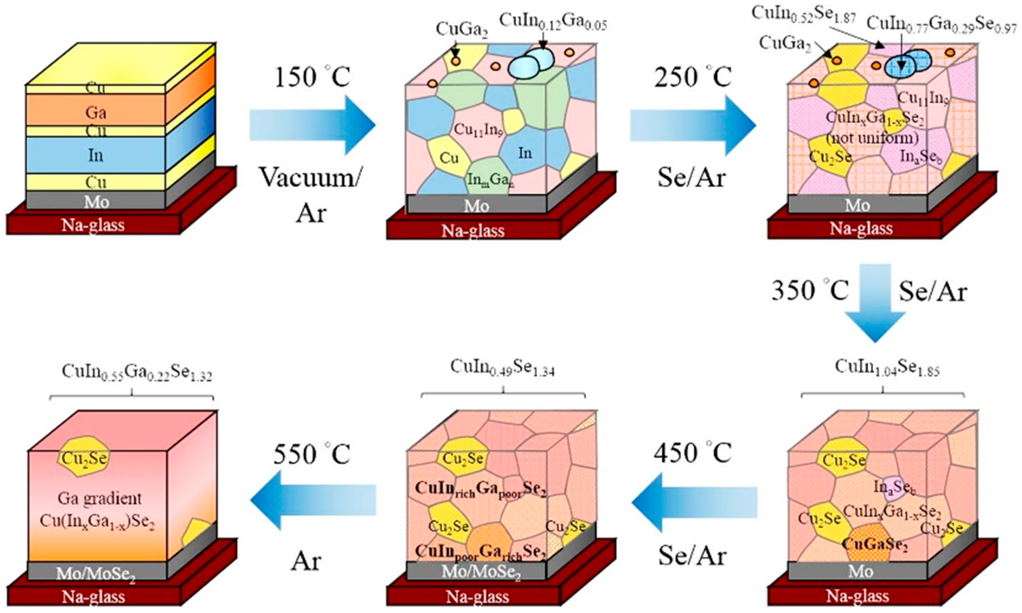
Yeh et al. studied the formation of CIGS produced with the two-stage selenization method [139,140,141]. The Cu-In-Ga precursor film consisting of Cu/In/Cu/Ga/Cu multilayers stacked in sequence from the substrate was deposited with the solutions of Cu2P2O7, InSO4 and Ga(OH)3, which provided the Cu, In and Ga sources, respectively. The deposited precursor film was immediately heated at 150 °C for 1 h in Ar to form alloyed phases in consideration of avoiding the precursor film from being oxidized. It was revealed that, with gradually increasing the selenization temperature, the composition of the precursor film experienced an evolution from a mixture containing multiple combinations of alloyed phases to a compound of CIGS. Figure 13 is a schematic diagram showing the process. This confirmed that a temperature of 550 °C is necessary for the formation of the CIGS compound. The produced film possessed a nearly stoichiometric composition of CuIn0.67Ga0.3Se2.03 [139].
The utilization of the electrodeposition technique for CIGS solar cells has proven to be very successful [142]. It was found that copper-poor CIGS with a [Cu/(In+Ga)] or CIG ratio of 0.8–0.9 and a [Ga/(In+Ga)] or GIG ratio of 0.3–0.35 is the preferred composition leading to a high solar cell efficiency, whereas copper-rich may result in a Cu-Se secondary phase, which diminishes the device performance [143]. Through optimizing the recipe of electrolyte and the parameters for deposition, electrodeposition has shown to be good at controlling the composition of CIGS. At present, electrodeposition (also known as electroplating) has been one of the primary methods adopted by the industry to manufacture CIGS solar cells. Table 1 summarizes the representative results of the solar cells constructed with electrodeposited CIGS. One can see that impressively high solar-to-power conversion efficiencies, for example, up to 17% for small solar cells and 12–14% for large cells, have been achieved. It is worth noting that, for solar cells, their performance is predominantly determined by the properties and quality of the absorber layer, e.g., the CIGS film in the CIGS solar cells. However, the overall solar-to-power conversion efficiency may also be greatly affected by other factors, such as the structure (or configuration) of the solar cell, the properties of other layers, the quality of interfaces and the front and rear contacts, and even the exposed area of the solar cell. Therefore, though the efficiencies are listed in Table 1 in increasing order, the efficiency increase does not exactly reflect the difference in the quality of the films or the parameters adopted to produce the films.

3.3.6. CZTS

Copper zinc tin sulfide (CZTS), Cu2ZnSnS4, was derivative from CIGS by changing indium by zinc and gallium by tin. CZTS also possesses a high absorption coefficient (>104 cm−1), a narrow bandgap, 1.45 eV, and more importantly the material consists of all earth abundant and non-toxic elements Cu, Zn, Sn and S, making it a potential photovoltaic material for low-cost, environmentally friendly solar cells [150,151,152]. The record efficiency of the CZTS solar cells is 11% so far achieved by Yan et al. in 2018 with the CZTS that was fabricated through co-sputtering Cu/ZnS/SnS followed by a sulfurization treatment [153] (note that another CZTS-based solar cell demonstrating a 12.6% efficiency reported by Wang et al. in 2019 actually used Cu2ZnSnSxSe4–x (CZTSSe), which contains Se [154]).
Similar to CIGS, CZTS can also be produced through the electrodeposition via a one-step co-deposition method or a two-stage sulfurization method.
(1)
One-Step Co-Deposition Method
The one-step co-deposition method uses an electrolyte containing the chlorides or sulfates of copper (e.g., CuCl or CuSO4), zinc (e.g., ZnCl2 or ZnSO4) and tin (e.g., SnCl4 or SnSO4) as the Cu, Zn and Sn sources, respectively, and typically Na2S2O3 as the S source. The deposition is usually carried out in an acidic electrolyte. Shinde et al. proposed that, when CuCl is employed as the Cu source (i.e., Cu(I)), the formation of CZTS resulted from the following reactions [155]:
2CuCl + ZnCl2 + SnCl4 + 8H2O → 2Cu+ + Zn2+ + Sn4+ + 8HCl + 8OH
4S2O32− → S4O62− + 4e
S2O32− + H+ → HSO3 + S
S + 2e → S2−
2Cu+ + Zn2+ + Sn4+ + 4S2− → Cu2ZnSnS4
In the case of CuSO4 as the Cu source (i.e., Cu(II)), Valdes et al. suggested that the overall reaction could be described as [18]:
Cu2+ + Zn2+ + Sn4+ + 2S2O32− + 12H+ + 18e → Cu2ZnSnS4 + 6H2O
With an electrolyte containing CuSO4, ZnSO4, SnSO4 and Na2S2O3 and using sodium citrate and tartaric acid as the complexing agents, at pH = 4–4.5 and the potential of −1.05 V vs. SCE, Pawar et al. produced CZTS successfully using the one-step co-deposition method. They found that, after heat treatment at 550 °C in Ar for 1 h, the deposited film turned to be crystalline and presented a kesterite structure, and the atomic ratios were revealed to be Cu:Zn:Sn:S = 22.98:10.35:11.21:55.46. Such a composition was perfectly close to the stoichiometric CZTS [156].
(2)
Two-Stage Sulfurization Method
Compared with the one-step co-deposition method, the two-stage sulfurization method has been more intensively used for the fabrication of CZTS films in the literature. The two-stage sulfurization method involves preparing a Cu-Sn-Zn precursor film through the electrodeposition first, and then sulfurizing the film in a sulfur (S) atmosphere, typically at 550 °C. The Cu-Sn-Zn precursor film can be either deposited in one solution that contains Cu, Sn and Zn salts (i.e., the so-called co-deposition) [157,158], or sequentially deposited in individual solutions of Cu, Sn and Zn to form a stacked layer structure [159]. Note that, in the latter case, the deposition should be in a Cu|Sn|Zn sequence in order to avoid the dissolution problem occurring to the early-deposited films.
He et al. prepared the stacked Cu-Sn-Zn precursor film using the electrolytes and the deposition parameters shown in Table 2 [159]. The reactions for the deposition of Cu, Sn and Zn can be described as follows:
Cu2+ + 2e → Cu E = 0.3419 V (SHE) − (RT/2F)ln[Cu2+]
Sn2+ + 2e → Sn E = −0.1375 V (SHE) − (RT/2F)ln[Sn2+]
Zn2+ + 2e → Zn E = −0.7618 V (SHE) − (RT/2F)ln[Zn2+]
where, E is the reduction potential, R the ideal gas constant, T the temperature and F the Faraday constant. It was found that, after a sulfurization treatment at 550 °C, the atomic ratios of Cu:Zn:Sn:S in the film were 24.66:13.18:11.97:50.l9. In another study also conducted by He et al., Cu-Sn-Zn precursor film was produced via co-deposition with a solution that contained Cu, Sn and Zn sources plus sodium citrate as the complexing agent [157]. The results revealed that, after a sulfurization treatment, the Cu:Zn:Sn:S ratios of the co-deposited CZTS were 24.36:12.45:12.46:50.73, which were almost the same as the ratios of the film with the Cu-Sn-Zn deposited sequentially.
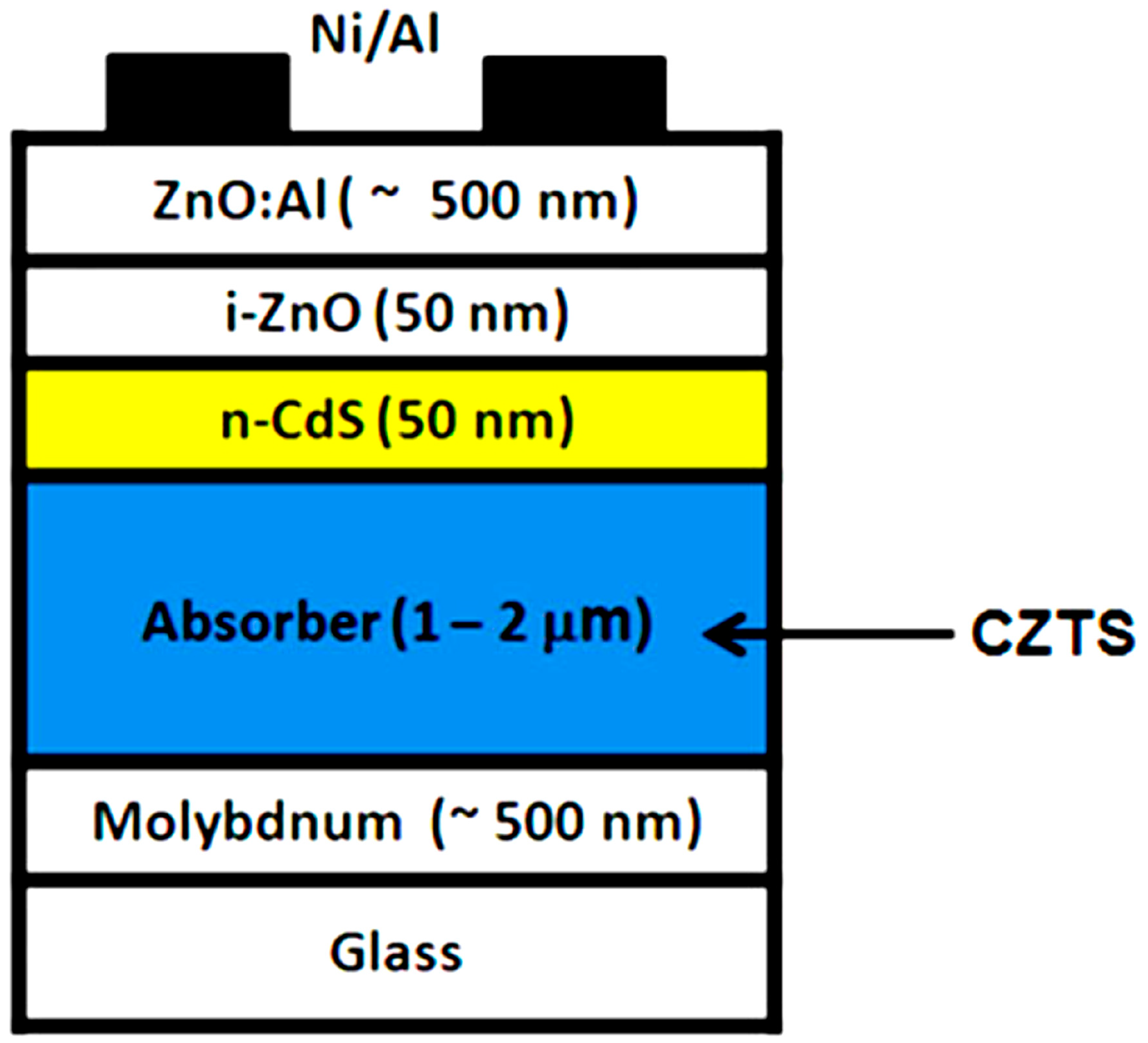
Figure 14 shows the typical structure of CZTS solar cells [160]. One can see that a CZTS solar cell is a structural analogue to a CIGS solar cell, in which the absorber layer uses CZTS. Table 3 summarizes the representative results of solar cells constructed with the electrodeposited CZTS films. It reveals that (1) the solar cell performance, or the quality of the CZTS film, is not necessarily related to the method used to create the precursor film; (2) the sulfurization treatment, which is typically carried out at a temperature of 560–585 °C, has been always conducted under an atmosphere that contains S (from elemental S or H2S), even if the precursor film is prepared with a one-step co-deposition method that already includes the deposition of S; (3) the pre-heat treatment of the precursor film is likely optional, though it was suggested that the treatment might enable the formation of metal alloys, which prevent oxidation of the films; (4) the composition of the CZTS film, which influences the crystal structure and electric property of the CZTS, plays a predominant role in affecting the quality of the CZTS and the performance of the solar cell, while the structure of the solar cell device is another important factor that affects the overall solar cell efficiency; in general, to achieve a high efficiency, the composition of the CZTS film should be Zn-rich and Cu-poor, or specifically the Cu/(Zn+Sn) and Zn/Sn ratios should lie in the range of 0.75–1 and 1–1.25, respectively [158] and (5) in addition to the Cu/(Zn+Sn) and Zn/Sn ratios, the ratio of S/metal also has an impact on the solar cell performance; it seems that the S/metal ratio should be greater than unity in order to achieve a high solar cell efficiency; however, there is a lack of sufficient information in literature in regard of this.

4. Concluding Remarks

(1)
The deposition potential must be selected carefully. The deposition potential is primarily determined by the standard electrode potential of cations and the recipe of the electrolyte that matters the concentration of the cations and the pH value of the electrolyte, but is also affected by some other factors such as the deposition temperature and the type of substrate (for example, FTO glass, ITO glass, stainless steel, copper or carbon). Cyclic voltammetry (CV) is the most effective way to help determine the deposition potential or understand the deposition mechanism.
(2)
It is always a challenge to balance the potential adopted for the deposition and the composition of the electrolyte (including the type of the complexing agent use in the electrolyte) in order to achieve the stoichiometric composition, especially in the case of ternary and quaternary chalcogenides. It seems that the stacked layer structure method is relatively advantageous in controlling the composition of the deposited films, in particular when the films consist of multiple elements and the deposition potentials of them are distributed in a wide range. However, since this method involves a sulfurization or selenization treatment of the precursor film comprised of metals, it is not ideal for the fabrication of thick films (>1 μm). In addition, the treatment is usually conducted at high temperatures, making the method not a good fit for most of the flexible substrates.
(3)
Complexing agents may have an important impact on the morphology and quality (e.g., the crystallinity and defects) of the deposited film by affecting the concentration of free cations in the electrolyte and thus affecting the deposition rate.
(4)
Post heat treatment is usually a necessary step to improve the crystallinity of the deposited films. Not only improving the crystallinity, depending on the atmosphere, post heat treatment can also function to adjust the composition of the films. Post heat treatment else contributes to growing the crystallites and enhancing the contact or adhesion between the deposited film and the substrate.
(5)
The use of ionic liquid- and organic solvent-based electrolytes may allow the deposition to be conducted at significantly higher temperatures, which is good for the formation of films with high quality and better crystallinity. However, compared with the aqueous electrolytes, the ionic liquid- and organic solvent-based electrolytes are usually less effective in dissolving inorganic salts. This limits the flexibility of choosing ideal reagents as the sources of elements for the film deposition.
(6)
Combining the electrodeposition with other techniques is a feasible way to make the deposited films gain improved quality. For example, the use of pulse potentials for the electrodeposition (known as pulsed electrodeposition) can result in better control of the composition and yield compact films [168]. Integrating electrophoretic [169] or chemical bath deposition [170] into the electrodeposition process may provide more flexibility in adjusting the film composition and, likely, may else lead to films with a more uniform morphology. Adding mechanical perturbations to the working electrode during the electrodeposition has also reported the capability in improving the film’s morphology [171].

5. Perspective

With the aim of making the electrodeposition a more ideal method for the fabrication of chalcogenide films towards high efficiency photovoltaic device applications, research in the following aspects is expected.
(1)
Developing more advanced electrolytes or new techniques to better control the composition of the deposited films, including eliminating the impurity and reducing the secondary phases in the films.
(2)
Exploring feasible methods to enhance the density of the deposited films and reduce the defects in the films. The relatively low density of the electrodeposited films and the existence of quite a large number of defects (e.g., the point defects and the planar defects at the grain boundaries) seem to be some of the major reasons that cause the solar cells constructed with the electrodeposited films generally less efficient than the cells that employ the films produced with a vacuum deposition method.
(3)
With regard to the ternary and quaternary chalcogenides, especially CIGS and CZTS, it is worth further developing the one-step co-deposition method, with the consideration of achieving selenization or sulfurization during the electrodeposition and thus simplifying the manufacturing operations to make the electrodeposition a more competitive technique in delivering low cost solar cells.
(4)
New ideas, for example, nanoparticle-based electrodeposition [172], photo-assisted electrodeposition [173], in situ monitoring of the deposition [174,175], may create the chances to gain better understanding of the kinetics of electrodeposition, make the control of the composition and microstructure of electrodeposited films more effective, and consequently deliver high quality films.
(5)
There is generally a lack of theoretical models to simulate the electrodeposition, in particular for the co-deposition of multiple elements. Machine learning is an emerging technology that may potentially be a great tool to predict the synthesis–composition–structure–property relationships of materials [176,177], including the films produced via electrodeposition.

Author Contributions

All authors contributed to gathering information from the literature and involved discussing and preparing the paper. All authors have read and agreed to the published version of the manuscript.

Funding

This work was supported in part by the North Dakota NASA EPSCoR Research Infrastructure Development (RID) Award. Zhang also thanks partial support from the National Science Foundation under Grant No. S&CC-1737538.

Acknowledgments

The authors would like to thank the NSF and ND NASA EPSCoR supports.

Conflicts of Interest

The authors declare no conflict of interest.

References

  1. Scheer, R.; Schock, H.-W. Chapter 4: Thin Film Material Properties. In Chalcogenide Photovoltaics: Physics, Technologies, and Thin Film Devices; John Wiley & Sons: Hoboken, NJ, USA, 2011; pp. 175–234. [Google Scholar]
  2. Fu, H. Environmentally friendly and earth-abundant colloidal chalcogenide nanocrystals for photovoltaic applications. J. Mater. Chem. C 2018, 6, 414–445. [Google Scholar] [CrossRef]
  3. Delbos, S. Kësterite thin films for photovoltaics: A review. EPJ Photovolt. 2012, 3, 35004. [Google Scholar] [CrossRef]
  4. Qurashi, A. Chapter 11: Solar Cell Application of Metal Chalcogenide Semiconductor Nanostructures. In Metal Chalcogenide Nanostructures for Renewable Energy Applications; John Wiley & Sons: Hoboken, NJ, USA, 2014; pp. 247–267. [Google Scholar]
  5. Lewis, D.J.; Kevin, P.; Bakr, O.; Muryn, C.A.; Malik, M.A.; O’Brien, P. Routes to tin chalcogenide materials as thin films or nanoparticles: A potentially important class of semiconductor for sustainable solar energy conversion. Inorg. Chem. Front. 2014, 1, 577–598. [Google Scholar] [CrossRef] [Green Version]
  6. Lee, T.D.; Ebong, A.U. A review of thin film solar cell technologies and challenges. Renew. Sustain. Energy Rev. 2017, 70, 1286–1297. [Google Scholar] [CrossRef]
  7. Powalla, M.; Paetel, S.; Ahlswede, E.; Wuerz, R.; Wessendorf, C.D.; Magorian Friedlmeier, T. Thin-film solar cells exceeding 22% solar cell efficiency: An overview on CdTe-, Cu(In,Ga)Se2-, and perovskite-based materials. Appl. Phys. Rev. 2018, 5, 041602. [Google Scholar] [CrossRef]
  8. Pal, K.; Singh, P.; Bhaduri, A.; Thapa, K.B. Current challenges and future prospects for a highly efficient (>20%) kesterite CZTS solar cell: A review. Solar Energy Mater. Solar Cells 2019, 196, 138–156. [Google Scholar] [CrossRef]
  9. Ji, S.; Ye, C. Cu2ZnSnS4 as a new solar cell material: The history and the future. Rev. Adv. Sci. Eng. 2012, 1, 42–58. [Google Scholar] [CrossRef]
  10. Zhou, H.; Hsu, W.-C.; Duan, H.-S.; Bob, B.; Yang, W.; Song, T.-B.; Hsu, C.-J.; Yang, Y. CZTS nanocrystals: A promising approach for next generation thin film photovoltaics. Energy Environ. Sci. 2013, 6, 2822–2838. [Google Scholar] [CrossRef]
  11. Shi, J.; Li, Z.; Zhang, D.; Liu, Q.; Sun, Z.; Huang, S. Fabrication of Cu(In,Ga)Se2 thin films by sputtering from a single quaternary chalcogenide target. Prog. Photovolt. Res. Appl. 2011, 19, 160–164. [Google Scholar] [CrossRef]
  12. Ramasamy, K.; Malik, M.A.; O’Brien, P. The chemical vapor deposition of Cu2ZnSnS4 thin films. Chem. Sci. 2011, 2, 1170–1172. [Google Scholar] [CrossRef]
  13. Rana, T.R.; Shinde, N.; Kim, J. Novel chemical route for chemical bath deposition of Cu2ZnSnS4 (CZTS) thin films with stacked precursor thin films. Mater. Lett. 2016, 162, 40–43. [Google Scholar] [CrossRef]
  14. Dona, J.; Herrero, J. Chemical bath deposition of CdS thin films: An approach to the chemical mechanism through study of the film microstructure. J. Electrochem. Soc. 1997, 144, 4081. [Google Scholar] [CrossRef]
  15. Kale, R.; Sartale, S.; Chougule, B.; Lokhande, C. Growth and characterization of nanocrystalline CdSe thin films deposited by the successive ionic layer adsorption and reaction method. Semicond. Sci. Technol. 2004, 19, 980. [Google Scholar] [CrossRef]
  16. Mali, S.S.; Patil, B.M.; Betty, C.A.; Bhosale, P.N.; Oh, Y.W.; Jadkar, S.R.; Devan, R.S.; Ma, Y.-R.; Patil, P.S. Novel synthesis of kesterite Cu2ZnSnS4 nanoflakes by successive ionic layer adsorption and reaction technique: Characterization and application. Electrochim. Acta 2012, 66, 216–221. [Google Scholar] [CrossRef]
  17. Wibowo, R.A.; Jung, W.H.; Kim, K.H. Synthesis of Cu2ZnSnSe4 compound powders by solid state reaction using elemental powders. J. Phys. Chem. Solids 2010, 71, 1702–1706. [Google Scholar] [CrossRef]
  18. Valdes, M.; Modibedi, M.; Mathe, M.; Hillie, T.; Vazquez, M. Electrodeposited Cu2ZnSnS4 thin films. Electrochim. Acta 2014, 128, 393–399. [Google Scholar] [CrossRef]
  19. Friedfeld, R.; Raffaelle, R.; Mantovani, J. Electrodeposition of CuInxGa1−xSe2 thin films. Sol. Energy Mater. Sol. Cells 1999, 58, 375–385. [Google Scholar] [CrossRef]
  20. Deligianni, H.; Ahmed, S.; Romankiw, L.T. The next frontier: Electrodeposition for solar cell fabrication. Electrochem. Soc. Interface 2011, 20, 47. [Google Scholar] [CrossRef]
  21. Kim, S.Y.; Kim, J. Fabrication of CIGS thin films by using spray pyrolysis and post-selenization. J. Korean Phys. Soc. 2012, 60, 2018–2024. [Google Scholar] [CrossRef]
  22. Kamoun, N.; Bouzouita, H.; Rezig, B. Fabrication and characterization of Cu2ZnSnS4 thin films deposited by spray pyrolysis technique. Thin Solid Films 2007, 515, 5949–5952. [Google Scholar] [CrossRef]
  23. Brenner, A. Part III: Introduction to Practical Considerations and Specific Information on the Electrodeposition of Alloys. In Electrodeposition of Alloys: Principles and Practice; Elsevier: Amsterdam, The Netherlands, 2013; pp. 409–678. [Google Scholar]
  24. Lincot, D. Electrodeposition of semiconductors. Thin Solid Films 2005, 487, 40–48. [Google Scholar] [CrossRef]
  25. Soare, V.; Burada, M.; Mitrica, D.; Badilita, V.; Stoiciu, F.; Lungu, C.; Ghenescu, V.; Rusu, M.; Antohe, Ş. Electrodeposition and characterization of CuInSe2/CdS multilayered thin films deposited on flexible substrate. Optoelectron. Adv. Mater. Rapid Commun. 2010, 4, 2018–2021. [Google Scholar]
  26. Mohammadzadeh, A.; Fox-Robichaud, A.; Selvaganapathy, P.R. Electroplating of Multiple Materials in Parallel Using Patterned Gels with Applications in Electrochemical Sensing. Sensors 2020, 20, 886. [Google Scholar] [CrossRef] [PubMed] [Green Version]
  27. Shaikh, A.V.; Mane, R.S.; Joo, O.-S.; Han, S.-H.; Pathan, H.M. Electrochemical deposition of cadmium selenide films and their properties: A review. J. Solid State Electrochem. 2017, 21, 2517–2530. [Google Scholar] [CrossRef]
  28. Mallik, A.; Ray, B. Evolution of principle and practice of electrodeposited thin film: A review on effect of temperature and sonication. Int. J. Electrochem. 2011, 2011, 568023. [Google Scholar] [CrossRef] [Green Version]
  29. Electric Double Layer. Available online: https://web.nmsu.edu/~snsm/classes/chem435/Lab14/double_layer.html (accessed on 20 August 2020).
  30. Zangari, G. Electrodeposition of alloys and compounds in the era of microelectronics and energy conversion technology. Coatings 2015, 5, 195–218. [Google Scholar] [CrossRef]
  31. Pandey, R.K.; Sahu, S.; Chandra, S. Chapter 3: Nucleation and Growth. In Handbook of Semiconductor Electrodeposition; M. Dekker: New York, NY, USA, 1996; pp. 61–88. [Google Scholar]
  32. Pasa, A.A.; Munford, M.L. Electrodeposition—Encyclopedia of Chemical Processing. Nova 2006, 821–832. [Google Scholar] [CrossRef]
  33. Raccichini, R.; Amores, M.; Hinds, G. Critical review of the use of reference electrodes in li-ion batteries: A diagnostic perspective. Batteries 2019, 5, 12. [Google Scholar] [CrossRef] [Green Version]
  34. Tatiparti, S.S.V.; Ebrahimi, F. Potentiostatic versus galvanostatic electrodeposition of nanocrystalline Al–Mg alloy powders. J. Solid State Electrochem. 2012, 16, 1255–1262. [Google Scholar] [CrossRef]
  35. Lou, H.H.; Huang, Y. Electroplating. Encyclopedia of Chemical Processing; Taylor & Francis: Oxfordshire, UK, 2006; pp. 1–10. [Google Scholar]
  36. Elgrishi, N.; Rountree, K.J.; McCarthy, B.D.; Rountree, E.S.; Eisenhart, T.T.; Dempsey, J.L. A practical beginner’s guide to cyclic voltammetry. J. Chem. Educ. 2018, 95, 197–206. [Google Scholar] [CrossRef]
  37. Fathy, M.; Kashyout, A.E.-H.B.; Elyamny, S.; Roston, G.D.; Bishara, A.A. Effect of CdCl2 concentration and heat treatment on electrodeposited nano-crystalline CdS thin films from non-aqueous solution. Int. J. Electrochem. Sci. 2014, 9, 6155–6165. [Google Scholar]
  38. Altiokka, B.; Yildirim, A.K. Electrodeposition of CdS thin films at various pH values. J. Korean Phys. Soc. 2018, 72, 687–691. [Google Scholar] [CrossRef]
  39. Lade, S.; Uplane, M.; Lokhande, C. Studies on the electrodeposition of CdS films. Mater. Chem. Phys. 1998, 53, 239–242. [Google Scholar] [CrossRef]
  40. Echendu, O.K.; Dejene, F.B.; Dharmadasa, I.M.; Eze, F.C. Characteristics of nanocrystallite-CdS produced by low-cost electrochemical technique for thin film photovoltaic application: The influence of deposition voltage. Int. J. Photoenergy 2017, 2017, 3989432. [Google Scholar] [CrossRef]
  41. Alam, A.; Cranton, W.; Dharmadasa, I. Electrodeposition of CdS thin-films from cadmium acetate and ammonium thiosulphate precursors. J. Mater. Sci. Mater. Electron. 2019, 30, 4580–4589. [Google Scholar] [CrossRef] [Green Version]
  42. Mammadov, M.; Aliyev, A.S.; Elrouby, M. Electrodeposition of cadmium sulfide. Int. J. Thin Film Sci. Technol. 2012, 1, 43–53. [Google Scholar]
  43. Baranski, A.S.; Fawcett, W.R.; McDonald, A.C.; de Nobriga, R.M.; MacDonald, J.R. The structural characterization of cadmium sulfide films grown by cathodic electrodeposition. J. Electrochem. Soc. 1981, 128, 963. [Google Scholar] [CrossRef]
  44. Lade, S.; Lokhande, C. Electrodeposition of CdS from non-aqueous bath. Mater. Chem. Phys. 1997, 49, 160–163. [Google Scholar] [CrossRef]
  45. Izgorodin, A.; Winther-Jensen, O.; Winther-Jensen, B.; MacFarlane, D.R. CdS thin-film electrodeposition from a phosphonium ionic liquid. Phys. Chem. Chem. Phys. 2009, 11, 8532–8537. [Google Scholar] [CrossRef]
  46. Hodes, G.; Manassen, J.; Cahen, D. Photoelectrochemical energy conversion and storage using polycrystalline chalcogenide electrodes. Nature 1976, 261, 403–404. [Google Scholar] [CrossRef]
  47. Kazacos, M.S.; Miller, B. Electrodeposition of CdSe films from selenosulfite solution. J. Electrochem. Soc. 1980, 127, 2378. [Google Scholar] [CrossRef]
  48. Teh, L.; Furin, V.; Martucci, A.; Guglielmi, M.; Wong, C.; Romanato, F. Electrodeposition of CdSe on nanopatterned pillar arrays for photonic and photovoltaic applications. Thin Solid Films 2007, 515, 5787–5791. [Google Scholar] [CrossRef]
  49. Sarangi, S.; Sahu, S. CdSe nanocrystalline thin films: Composition, structure and optical properties. Phys. E Low-Dimens. Syst. Nanostruct. 2004, 23, 159–167. [Google Scholar] [CrossRef]
  50. Szabo, J.P.; Cocivera, M. Mechanism of electrodeposition of cadmium selenide from solution. Can. J. Chem. 1988, 66, 1065–1072. [Google Scholar] [CrossRef]
  51. Bouroushian, M. Chapter 3: Electrochemical Preparations—Conventional Coatings and Structures. In Electrochemistry of Metal Chalcogenides; Springer Science & Business Media: Berlin/Heidelberg, Germany, 2010; pp. 76–152. [Google Scholar]
  52. Dale, P.J.; Samantilleke, A.P.; Shivagan, D.D.; Peter, L.M. Synthesis of cadmium and zinc semiconductor compounds from an ionic liquid containing choline chloride and urea. Thin Solid Films 2007, 515, 5751–5754. [Google Scholar] [CrossRef]
  53. Kariper, I.; Bağlayan, O.; Gode, F. Fabrication and optical characterization of CdSe thin films grown by chemical bath deposition. Acta Phys. Pol. A 2015, 128, B-219–B-221. [Google Scholar] [CrossRef]
  54. Park, J.H.; Wang, Q.; Zhu, K.; Frank, A.J.; Kim, J.Y. Electrochemical Deposition of Conformal Semiconductor Layers in Nanoporous Oxides for Sensitized Photoelectrodes. ACS Omega 2019, 4, 19772–19776. [Google Scholar] [CrossRef] [Green Version]
  55. Alkire, R.C.; Kolb, D.M.; Lipkowski, J.; Ross, P.N. Chapter 2: Tailoring of Interfaces for the Photoelectrochemical Conversion of Solar Energy. In Photoelectrochemical Materials and Energy Conversion Processes; John Wiley & Sons: Hoboken, NJ, USA, 2010; Volume 24, pp. 61–181. [Google Scholar]
  56. Chowdhury, R.; Islam, M.; Sabeth, F.; Mustafa, G.; Farhad, S.; Saha, D.; Chowdhury, F.; Hussain, S.; Islam, A. Characterization of electrodeposited cadmium selenide thin films. Dhaka Univ. J. Sci. 2012, 60, 137–140. [Google Scholar] [CrossRef]
  57. Pawar, S.; Moholkar, A.; Bhosale, C. Influence of pH on electrochemically deposited CdSe thin films. Mater. Lett. 2007, 61, 1034–1038. [Google Scholar] [CrossRef]
  58. Rashwan, S.; Abd El-Wahab, S.; Mohamed, M. Electrodeposition and characterization of CdSe semiconductor thin films. J. Mater. Sci. Mater. Electron. 2007, 18, 575–585. [Google Scholar] [CrossRef]
  59. Baubinas, R.; Januškevičius, Z.; Sakalas, A. CdSe single crystals with n-and p-type of conductivity approaching intrinsic. Mater. Res. Bull. 1973, 8, 817–823. [Google Scholar] [CrossRef]
  60. Ohtsuka, T.; Kawamata, J.; Zhu, Z.; Yao, T. p-type CdSe grown by molecular beam epitaxy using a nitrogen plasma source. Appl. Phys. Lett. 1994, 65, 466–468. [Google Scholar] [CrossRef]
  61. Diso, D.; Fauzi, F.; Echendu, O.; Olusola, O.; Dharmadasa, I. Optimisation of CdTe electrodeposition voltage for development of CdS/CdTe solar cells. J. Mater. Sci. Mater. Electron. 2016, 27, 12464–12472. [Google Scholar] [CrossRef]
  62. Rastogi, A.; Sharma, R. Properties and mechanism of solar absorber CdTe thin film synthesis by unipolar galvanic pulsed electrodeposition. J. Appl. Electrochem. 2009, 39, 167–176. [Google Scholar] [CrossRef]
  63. Duffy, N.; Peter, L.; Wang, R.; Lane, D.; Rogers, K. Electrodeposition and characterisation of CdTe films for solar cell applications. Electrochim. Acta 2000, 45, 3355–3365. [Google Scholar] [CrossRef]
  64. Sella, C.; Boncorps, P.; Vedel, J. The electrodeposition mechanism of CdTe from acidic aqueous solutions. J. Electrochem. Soc. 1986, 133, 2043. [Google Scholar] [CrossRef]
  65. Bhattacharya, R.; Rajeshwar, K. Electrodeposition of CdTe thin films. J. Electrochem. Soc. 1984, 131, 2032. [Google Scholar] [CrossRef]
  66. Patil, V.; Sutrave, D.; Shahane, G.; Deshmukh, L. Cadmium telluride thin films: Growth from solution and characteristics. Thin Solid Films 2001, 401, 35–38. [Google Scholar] [CrossRef]
  67. Dharmadasa, I.; Bingham, P.A.; Echendu, O.; Salim, H.; Druffel, T.; Dharmadasa, R.; Sumanasekera, G.; Dharmasena, R.; Dergacheva, M.; Mit, K. Fabrication of CdS/CdTe-based thin film solar cells using an electrochemical technique. Coatings 2014, 4, 380–415. [Google Scholar] [CrossRef]
  68. Diso, D.G. Research and Development of CdTe Based Thin Film PV Solar Cells. Ph.D. Thesis, Sheffield Hallam University, Sheffield, UK, 2011. [Google Scholar]
  69. Takahashi, M.; Uosaki, K.; Kita, H.; Yamaguchi, S. Resistivity, carrier concentration, and carrier mobility of electrochemically deposited CdTe films. J. Appl. Phys. 1986, 60, 2046–2049. [Google Scholar] [CrossRef] [Green Version]
  70. Echendu, O.; Okeoma, K.; Oriaku, C.; Dharmadasa, I. Electrochemical deposition of CdTe semiconductor thin films for solar cell application using two-electrode and three-electrode configurations: A comparative study. Adv. Mater. Sci. Eng. 2016, 2016, 3581725. [Google Scholar] [CrossRef] [Green Version]
  71. Duffy, N.; Peter, L.; Wang, R. Characterisation of CdS∣ CdTe heterojunctions by photocurrent spectroscopy and electrolyte electroreflectance/absorbance spectroscopy (EEA/EER). J. Electroanal. Chem. 2002, 532, 207–214. [Google Scholar] [CrossRef]
  72. Bonilla, S.; Dalchiele, E.A. Electrochemical deposition and characterization of CdTe polycrystalline thin films. Thin Solid Films 1991, 204, 397–403. [Google Scholar] [CrossRef]
  73. Asabe, M.; Ubale, V.; Manikshete, A.; Vader, V.; Rajmane, S.; Delekar, S. Properties of electrochemically deposited CdTe thin films: Annealing effect. J. Mater. Sci. Mater. Electron. 2013, 24, 4655–4661. [Google Scholar] [CrossRef]
  74. Shenouda, A.Y.; El Sayed, M. Electrodeposition, characterization and photo electrochemical properties of CdSe and CdTe. Ain Shams Eng. J. 2015, 6, 341–346. [Google Scholar] [CrossRef] [Green Version]
  75. Echendu, O.; Dejene, B.; Hone, F. Comparative performance of CdS/CdTe thin film solar cells fabricated with electrochemically deposited CdTe from 2-electrode and 3-electrode set-ups. Mater. Sci. Eng. B 2018, 232, 55–60. [Google Scholar] [CrossRef]
  76. Ray, A. Electrodeposition of thin films for low-cost solar cells. In Electroplat. of Nanostructures; InTech: Rijeka, Croatia, 2015. [Google Scholar]
  77. Major, J.; Treharne, R.; Phillips, L.; Durose, K. A low-cost non-toxic post-growth activation step for CdTe solar cells. Nature 2014, 511, 334–337. [Google Scholar] [CrossRef]
  78. Zhang, W.; Liu, J.; Guo, Z.; Yao, S.; Wang, H. Synthesis and characterization of CdTe nanoparticle-sensitized TiO 2 nanotube arrays for photocatalysis. J. Mater. Sci. Mater. Electron. 2017, 28, 9505–9513. [Google Scholar] [CrossRef]
  79. Zhang, Y.; Wu, W.; Liu, Y.; Yang, W.; Chen, W.; Zhao, J. Alkaline electrolyte: Toward high-quality CdTe films with the assistance of strong complexing agent and organic base. CrystEngComm 2018, 20, 8–11. [Google Scholar] [CrossRef]
  80. Cho, D.H.; Lee, W.J.; Wi, J.H.; Han, W.S.; Kim, T.G.; Kim, J.W.; Chung, Y.D. Interface analysis of Cu(In,Ga)Se2 and ZnS formed using sulfur thermal cracker. ETRI J. 2016, 38, 265–271. [Google Scholar] [CrossRef] [Green Version]
  81. Lukianova, O.; Klochko, N.; Khrypunov, G.; Kopach, V.; Lyubov, V. Development of n-ZnS/p-Cu2ZnSnS4 heterojunction for thin film solar cells. In Proceedings of the 2016 International Conference on Nanomaterials: Application & Properties (NAP), Lviv, Ukraine, 14–19 September 2016; pp. 02NEA05-01–02NEA05-03. [Google Scholar]
  82. Mkawi, E.; Ibrahim, K.; Ali, M.; Farrukh, M.; Mohamed, A. Electrodeposited ZnS precursor layer with improved electrooptical properties for efficient Cu2ZnSnS4 thin-film solar cells. J. Electron. Mater. 2015, 44, 3380–3387. [Google Scholar] [CrossRef]
  83. Lokhande, C.; Jadhav, M.; Pawar, S. Electrodeposition of ZnS films from an alkaline bath. J. Electrochem. Soc. 1989, 136, 2756–2757. [Google Scholar] [CrossRef]
  84. Zhu, H.; Huang, J.; Wang, Y.; Cao, L.; He, H.; Wu, J. Synthesis and characterisation of ZnS optical thin films through cathodic electrodeposition technique. Surf. Eng. 2011, 27, 42–45. [Google Scholar] [CrossRef]
  85. Matsuda, N.; Okamoto, N.; Saito, T. Electrodeposition of ZnS and evaluation of its optical property. In Proceedings of the 2018 International Conference on Electronics Packaging and iMAPS All Asia Conference (ICEP-IAAC), Kuwana, Japan, 17–21 April 2018; pp. 566–569. [Google Scholar]
  86. Madugu, M.L.; Olusola, O.I.-O.; Echendu, O.K.; Kadem, B.; Dharmadasa, I.M. Intrinsic doping in electrodeposited ZnS thin films for application in large-area optoelectronic devices. J. Electron. Mater. 2016, 45, 2710–2717. [Google Scholar] [CrossRef]
  87. Zakerian, F.; Kafashan, H. Investigation the effect of annealing parameters on the physical properties of electrodeposited ZnS thin films. Superlattices Microstruct. 2018, 124, 92–106. [Google Scholar] [CrossRef]
  88. Hassane, B.; Benmoussa, D. Investigation of Absorber Layer Thickness Effect on CIGS Solar Cell in Different Cases of Buffer Layers. J. Nano Electron. Phys. 2018, 10, 1–2. [Google Scholar] [CrossRef]
  89. Ohtake, Y.; Kushiya, K.; Ichikawa, M.; Yamada, A.; Konagai, M. Polycrystalline Cu(InGa)Se2 thin-film solar cells with ZnSe buffer layers. Jpn. J. Appl. Phys. 1995, 34, 5949. [Google Scholar] [CrossRef]
  90. Konagai, M.; Ohtake, Y.; Okamoto, T. Development of Cu(InGa)Se2 Thin Film Solar Cells with Cd-Free Buffer Layers. MRS Online Proc. Libr. Arch. 1996, 426, 153. [Google Scholar] [CrossRef]
  91. Chandramohan, R.; Sanjeeviraja, C.; Mahalingam, T. Preparation of zinc selenide thin films by electrodeposition technique for solar cell applications. Phys. Status Solidi A Appl. Res. 1997, 163, R11–R12. [Google Scholar] [CrossRef]
  92. Kathalingam, A.; Mahalingam, T.; Sanjeeviraja, C. Optical and structural study of electrodeposited zinc selenide thin films. Mater. Chem. Phys. 2007, 106, 215–221. [Google Scholar] [CrossRef]
  93. Natarajan, C.; Sharon, M.; Levy-Clement, C.; Neumann-Spallart, M. Electrodeposition of zinc selenide. Thin Solid Films 1994, 237, 118–123. [Google Scholar] [CrossRef]
  94. Kowalik, R.; Żabiński, P.; Fitzner, K. Electrodeposition of ZnSe. Electrochim. Acta 2008, 53, 6184–6190. [Google Scholar] [CrossRef]
  95. Rusu, G.; Diciu, M.; Pirghie, C.; Popa, E. Structural characterization and optical properties of ZnSe thin films. Appl. Surf. Sci. 2007, 253, 9500–9505. [Google Scholar] [CrossRef]
  96. Laks, D.; Van de Walle, C.; Neumark, G.; Blöchl, P.; Pantelides, S. Native defects and self-compensation in ZnSe. Phys. Rev. B 1992, 45, 10965. [Google Scholar] [CrossRef] [PubMed] [Green Version]
  97. Manzoli, A.; Eguiluz, K.; Salazar-Banda, G.; Machado, S. Electrodeposition and characterization of undoped and nitrogen-doped ZnSe films. Mater. Chem. Phys. 2010, 121, 58–62. [Google Scholar] [CrossRef]
  98. Gromboni, M.F.; Mascaro, L.H. Optical and structural study of electrodeposited zinc selenide thin films. J. Electroanal. Chem. 2016, 780, 360–366. [Google Scholar] [CrossRef]
  99. Samantilleke, A.; Boyle, M.; Young, J.; Dharmadasa, I. Electrodeposition of n-type and p-type ZnSe thin films for applications in large area optoelectronic devices. J. Mater. Sci. Mater. Electron. 1998, 9, 289–290. [Google Scholar] [CrossRef]
  100. Jun, Y.; Kim, K.-J.; Kim, D. Electrochemical synthesis of Cu-doped ZnTe films as back contacts to CdTe solar cells. Met. Mater. 1999, 5, 279–285. [Google Scholar] [CrossRef]
  101. Tang, J.; Mao, D.; Feng, L.; Song, W.; Trefny, J. The properties and optimization of ZnTe: Cu back contacts on CdTe/CdS thin film solar cells. In Proceedings of the Conference Record of the Twenty Fifth IEEE Photovoltaic Specialists Conference-1996, Washington, DC, USA, 13–17 May 1996; pp. 925–928. [Google Scholar]
  102. Mondal, A.; McCandless, B.E.; Birkmire, R.W. Electrochemical deposition of thin ZnTe films as a contact for CdTe solar cells. Sol. Energy Mater. Sol. Cells 1992, 26, 181–187. [Google Scholar] [CrossRef]
  103. Mahalingam, T.; John, V.; Rajendran, S.; Sebastian, P. Electrochemical deposition of ZnTe thin films. Semicond. Sci. Technol. 2002, 17, 465. [Google Scholar] [CrossRef]
  104. Skhouni, O.; El Manouni, A.; Mollar, M.; Schrebler, R.; Marí, B. ZnTe thin films grown by electrodeposition technique on Fluorine Tin Oxide substrates. Thin Solid Films 2014, 564, 195–200. [Google Scholar] [CrossRef]
  105. Bouroushian, M.; Kosanovic, T.; Karoussos, D.; Spyrellis, N. Electrodeposition of polycrystalline ZnTe from simple and citrate-complexed acidic aqueous solutions. Electrochim. Acta 2009, 54, 2522–2528. [Google Scholar] [CrossRef]
  106. Hossain, M.; Siddiquee, K.; Islam, O.; Gafur, M.; Qadir, M.; Ahmed, N. Characterization of electrodeposited ZnTe thin films. J. Opt. 2019, 48, 295–301. [Google Scholar] [CrossRef]
  107. Catrangiu, A.; Beregoi, M.; Cojocaru, A.; Anicai, L.; Cotarta, A.; Visan, T. Electrochemical Deposition of Zinc Telluride Thin Films from Ethaline Ionic Liquid. Chalcogenide Lett. 2016, 13, 187–199. [Google Scholar]
  108. Coughlan, C.; Ibanez, M.; Dobrozhan, O.; Singh, A.; Cabot, A.; Ryan, K.M. Compound copper chalcogenide nanocrystals. Chem. Rev. 2017, 117, 5865–6109. [Google Scholar] [CrossRef]
  109. Lippkow, D.; Strehblow, H.-H. Structural investigations of thin films of copper–selenide electrodeposited at elevated temperatures. Electrochim. Acta 1998, 43, 2131–2140. [Google Scholar] [CrossRef]
  110. Dergacheva, M.; Chaikin, V.; Grigor’eva, V.; Pantileeva, E. Electrodeposition of CuSex compounds onto carbon-containing electrodes. Russ. J. Appl. Chem. 2004, 77, 1273–1278. [Google Scholar] [CrossRef]
  111. Grozdanov, I. Electroconductive copper selenide films on transparent polyester sheets. Synth. Met. 1994, 63, 213–216. [Google Scholar] [CrossRef]
  112. He, W.; Zhang, H.; Zhang, Y.; Liu, M.; Zhang, X.; Yang, F. Electrodeposition and characterization of CuTe and Cu2Te thin films. J. Nanomater. 2015, 2015, 240525. [Google Scholar] [CrossRef] [Green Version]
  113. Jeyakumar, P.; Thanikaikarasan, S.; Natarajan, B. Role of substrate in electrodeposited copper telluride thin films. J. Mater. Sci. Mater. Electron. 2017, 28, 2538–2544. [Google Scholar] [CrossRef]
  114. Ghosh, A.; Mitra, M.; Banerjee, D.; Mondal, A. Facile electrochemical deposition of Cu7Te4 thin films with visible-light driven photocatalytic activity and thermoelectric performance. RSC Adv. 2016, 6, 22803–22811. [Google Scholar] [CrossRef]
  115. Uda, H.; Ikegami, S.; Sonomura, H. Annealing effect of Cu2TeAu contact to evaporated CdTe film on photovoltaic properties of CdS/CdTe solar cell. Sol. Energy Mater. Sol. Cells 1998, 50, 141–146. [Google Scholar] [CrossRef]
  116. Kim, S.; Jeon, J.; Suh, J.; Hong, J.; Kim, T.; Kim, K.; Cho, S. Comparative Study of Cu2Te and Cu Back Contact in CdS/CdTe Solar Cell. J. Korean Phys. Soc. 2018, 72, 780–785. [Google Scholar] [CrossRef]
  117. Golgovici, F.; Catrangiu, A.-S.; Visan, T. The Formation and Characterization of Copper Telluride Films from Choline Chloride–Urea Ionic Liquid. Int. J. Electrochem. Sci. 2016, 11, 915–928. [Google Scholar]
  118. Catrangiu, A.-S.; Sin, I.; Prioteasa, P.; Cotarta, A.; Cojocaru, A.; Anicai, L.; Visan, T. Studies of antimony telluride and copper telluride films electrodeposition from choline chloride containing ionic liquids. Thin Solid Films 2016, 611, 88–100. [Google Scholar] [CrossRef]
  119. Kashyout, A.-H.; Ahmed, E.-Z.; Meaz, T.; Nabil, M.; Amer, M. (One-step) electrochemical deposition and characterization of CuInSe2 thin films. Alex. Eng. J. 2014, 53, 731–736. [Google Scholar] [CrossRef] [Green Version]
  120. Guillemoles, J.F.; Cowache, P.; Lusson, A.; Fezzaa, K.; Boisivon, F.; Vedel, J.; Lincot, D. One step electrodeposition of CuInSe2: Improved structural, electronic, and photovoltaic properties by annealing under high selenium pressure. J. Appl. Phys. 1996, 79, 7293–7302. [Google Scholar] [CrossRef]
  121. Ulleh, S.; Mollar, M.; Marí, B.; Ullah, H.; Ghannam, H.; Chahboun, A. The Effect of Defects on the Overall Performance of CuInSe2/CdS/ZnO Thin Film Solar Cells. In Proceedings of the 2017 International Renewable and Sustainable Energy Conference (IRSEC), Tangier, Morocco, 4–7 December 2017; pp. 1–4. [Google Scholar]
  122. Hernandez-Pagan, E.A.; Wang, W.; Mallouk, T.E. Template electrodeposition of single-phase p-and n-type copper indium diselenide (CuInSe2) nanowire arrays. ACS Nano 2011, 5, 3237–3241. [Google Scholar] [CrossRef]
  123. Fischer, J.; Larsen, J.K.; Guillot, J.; Aida, Y.; Eisenbarth, T.; Regesch, D.; Depredurand, V.; Fevre, N.; Siebentritt, S.; Dale, P.J. Composition dependent characterization of copper indium diselenide thin film solar cells synthesized from electrodeposited binary selenide precursor stacks. Sol. Energy Mater. Sol. Cells 2014, 126, 88–95. [Google Scholar] [CrossRef]
  124. Chiang, C.-S.; Lee, W.; Chang, T.; Su, Y. Improving conversion efficiency of co-electrodeposited CuInSe2 thin film solar cells with substrate and solution heating. J. Appl. Electrochem. 2015, 45, 549–556. [Google Scholar] [CrossRef]
  125. Dale, P.; Samantilleke, A.; Zoppi, G.; Forbes, I.; Peter, L. Characterization of CuInSe2 material and devices: Comparison of thermal and electrochemically prepared absorber layers. J. Phys. D Appl. Phys. 2008, 41, 085105. [Google Scholar] [CrossRef]
  126. Londhe, P.U.; Rohom, A.B.; Chaure, N.B. CuInSe2 thin film solar cells prepared by low-cost electrodeposition techniques from a non-aqueous bath. RSC Adv. 2015, 5, 89635–89643. [Google Scholar] [CrossRef]
  127. Mahalingam, T.; Thanikaikarasan, S.; Sanjeeviraja, C.; Kim, T.; Sebastian, P.; Kim, Y.D. Studies on Electroplated Copper Indium Telluride Thin Films. J. New Mater. Electrochem. Syst. 2010, 13, 77–82. [Google Scholar]
  128. Lakhe, M.; Chaure, N.B. Characterization of electrochemically deposited CuInTe2 thin films for solar cell applications. Sol. Energy Mater. Sol. Cells 2014, 123, 122–129. [Google Scholar] [CrossRef]
  129. Prasher, D.; Dhakad, K.; Thakur, V.; Rajaram, P. Electrochemical Growth and Studies of Indium-Rich CuInTe2 Thin Films. Int. J. Mater. Sci. Appl. 2014, 3, 1. [Google Scholar] [CrossRef] [Green Version]
  130. Lakhe, M.; Mahapatra, S.; Chaure, N.B. Development of CuInTe2 thin film solar cells by electrochemical route with low temperature (80 °C) heat treatment procedure. Mater. Sci. Eng. B 2016, 204, 20–26. [Google Scholar] [CrossRef]
  131. Lakhe, M.; Chaure, N. Low-temperature Heat Treatment (80 °C) Effect on the Electrochemically Synthesized CuInTe2 Thin Films for Energy Harvesting Applications. J. Mater. Sci. Eng. 2015, 4, 1000204 (1–6). [Google Scholar] [CrossRef] [Green Version]
  132. Saji, V.S.; Lee, S.-M.; Lee, C.W. CIGS thin film solar cells by electrodeposition. J. Korean Electrochem. Soc. 2011, 14, 61–70. [Google Scholar] [CrossRef]
  133. Lincot, D.; Guillemoles, J.-F.; Taunier, S.; Guimard, D.; Sicx-Kurdi, J.; Chaumont, A.; Roussel, O.; Ramdani, O.; Hubert, C.; Fauvarque, J. Chalcopyrite thin film solar cells by electrodeposition. Sol. Energy 2004, 77, 725–737. [Google Scholar] [CrossRef]
  134. Bhattacharya, R.N.; Oh, M.-K.; Kim, Y. CIGS-based solar cells prepared from electrodeposited precursor films. Sol. Energy Mater. Sol. Cells 2012, 98, 198–202. [Google Scholar] [CrossRef]
  135. Long, F.; Wang, W.; Du, J.; Zou, Z. CIS (CIGS) thin films prepared for solar cells by one-step electrodeposition in alcohol solution. J. Phys. Conf. Ser. 2009, 152, 012074. [Google Scholar] [CrossRef]
  136. Lian, Y.; Zhang, J.; Ma, X.; Yang, P.; An, M. Synthesizing three-dimensional ordered macroporous CuInxGa1−xSe2 thin films by template-assisted electrodeposition from modified ionic liquid. Ceram. Int. 2018, 44, 2599–2602. [Google Scholar] [CrossRef]
  137. Lian, Y.; Ji, S.; Zhao, L.; Zhang, J.; Yang, P.; Zhang, J.; An, M. One-step electrodeposition of CuInxGa1−x Se2 thin films from a mixture system of ionic liquid and ethanol. New J. Chem. 2015, 39, 7742–7745. [Google Scholar] [CrossRef]
  138. Lian, Y.; Liu, A.; Ma, X.; Zhang, J.; Yang, P.; An, M. A Mixture of Ionic Liquid and Ethanol Used for Galvanostatic Electrodeposition of CuInxGa1-xSe2 Thin Films. J. Electrochem. Soc. 2017, 164, D969. [Google Scholar] [CrossRef]
  139. Yeh, M.-H.; Hsu, H.-R.; Wang, K.-C.; Ho, S.-J.; Chen, G.-H.; Chen, H.-S. Toward low-cost large-area CIGS thin film: Compositional and structural variations in sequentially electrodeposited CIGS thin films. Sol. Energy 2016, 125, 415–425. [Google Scholar] [CrossRef]
  140. Yeh, M.-H.; Ho, S.-J.; Wang, K.-C.; Hsu, H.-R.; Chen, G.-H.; Chen, H.-S. Toward low-cost large-area CIGS thin film II: Out-of-plane compositional variations of sequentially electrodeposited Cu/In/Cu/Ga/Cu stacked layers selenized in rapid thermal process. Sol. Energy 2016, 129, 116–125. [Google Scholar] [CrossRef]
  141. Yeh, M.-H.; Ho, S.-J.; Chen, G.-H.; Yeh, C.-W.; Chen, P.-R.; Chen, H.-S. Toward low-cost large-area CIGS thin film III: Effect of Se concentration on crystal growth and defect formation of sequentially electrodeposited CIGS thin films. Sol. Energy 2016, 132, 547–557. [Google Scholar] [CrossRef]
  142. Farooq, L.; Alraeesi, A.; Al Zahmi, S. A review on the Electrodeposition of CIGS Thin-Film Solar Cells. In Proceedings of the International Conference on Industrial Engineering and Operations Management, Riyadh, Saudi Arabia, 26–28 November 2019. [Google Scholar]
  143. Chandran, R.; Panda, S.K.; Mallik, A. A short review on the advancements in electroplating of CuInGaSe2 thin films. Mater. Renew. Sustain. Energy 2018, 7, 6. [Google Scholar]
  144. Londhe, P.U.; Rohom, A.B.; Fernandes, R.; Kothari, D.; Chaure, N.B. Development of superstrate CuInGaSe2 thin film solar cells with low-cost electrochemical route from nonaqueous bath. ACS Sustain. Chem. Eng. 2018, 6, 4987–4995. [Google Scholar] [CrossRef]
  145. Bhattacharya, R.N. CIGS-based solar cells prepared from electrodeposited stacked Cu/In/Ga layers. Sol. Energy Mater. Sol. Cells 2013, 113, 96–99. [Google Scholar] [CrossRef]
  146. Başol, B.; Pinarbaşi, M.; Aksu, S.; Freitag, J.; Gonzalez, P.; Johnson, T.; Matus, Y.; Metin, B.; Narasimhan, M.; Nayak, D. Status of electroplating based CIGS technology development. In Proceedings of the 34th IEEE Photovoltaic Specialists Conference (PVSC 2009), Philadelphia, PA, USA, 7–12 June 2009; pp. 002310–002315. [Google Scholar]
  147. Duchatelet, A.; Sidali, T.; Loones, N.; Savidand, G.; Chassaing, E.; Lincot, D. 12.4% Efficient Cu(In,Ga)Se2 solar cell prepared from one step electrodeposited Cu–In–Ga oxide precursor layer. Sol. Energy Mater. Sol. Cells 2013, 119, 241–245. [Google Scholar] [CrossRef]
  148. Duchatelet, A.; Letty, E.; Jaime-Ferrer, S.; Grand, P.-P.; Mollica, F.; Naghavi, N. The impact of reducing the thickness of electrodeposited stacked Cu/In/Ga layers on the performance of CIGS solar cells. Sol. Energy Mater. Sol. Cells 2017, 162, 114–119. [Google Scholar] [CrossRef]
  149. Broussillou, C.; Viscogliosi, C.; Rogee, A.; Angle, S.; Grand, P.; Bodnar, S.; Debauche, C.; Allary, J.; Bertrand, B.; Guillou, C. Statistical Process Control for Cu(In,Ga)(S,Se)2 electrodeposition-based manufacturing process of 60 × 120 cm2 modules up to 14.0% efficiency. In Proceedings of the IEEE 42nd Photovoltaic Specialist Conference (PVSC 2015), New Orleans, LA, USA, 14–19 June 2015; pp. 1–5. [Google Scholar]
  150. Ravindiran, M.; Praveenkumar, C. Status review and the future prospects of CZTS based solar cell–A novel approach on the device structure and material modeling for CZTS based photovoltaic device. Renew. Sustain. Energy Rev. 2018, 94, 317–329. [Google Scholar] [CrossRef]
  151. Giraldo, S.; Jehl, Z.; Placidi, M.; Izquierdo-Roca, V.; Pérez-Rodríguez, A.; Saucedo, E. Progress and perspectives of thin film kesterite photovoltaic technology: A critical review. Adv. Mater. 2019, 31, 1806692. [Google Scholar] [CrossRef] [PubMed] [Green Version]
  152. Sharmin, A.; Bashar, M.; Sultana, M.; Al Mamun, S.M. Sputtered single-phase kesterite Cu2ZnSnS4(CZTS) thin film for photovoltaic applications: Post annealing parameter optimization and property analysis. AIP Adv. 2020, 10, 015230. [Google Scholar] [CrossRef] [Green Version]
  153. Yan, C.; Huang, J.; Sun, K.; Johnston, S.; Zhang, Y.; Sun, H.; Pu, A.; He, M.; Liu, F.; Eder, K. Cu2ZnSnS4 solar cells with over 10% power conversion efficiency enabled by heterojunction heat treatment. Nat. Energy 2018, 3, 764–772. [Google Scholar] [CrossRef]
  154. Wang, W.; Winkler, M.T.; Gunawan, O.; Gokmen, T.; Todorov, T.K.; Zhu, Y.; Mitzi, D.B. Device characteristics of CZTSSe thin-film solar cells with 12.6% efficiency. Adv. Energy Mater. 2014, 4, 1301465. [Google Scholar] [CrossRef]
  155. Shinde, N.; Lokhande, C.; Kim, J.; Moon, J. Low cost and large area novel chemical synthesis of Cu2ZnSnS4 (CZTS) thin films. J. Photochem. Photobiol. A Chem. 2012, 235, 14–20. [Google Scholar] [CrossRef]
  156. Pawar, S.; Pawar, B.; Moholkar, A.; Choi, D.; Yun, J.; Moon, J.; Kolekar, S.; Kim, J. Single step electrosynthesis of Cu2ZnSnS4 (CZTS) thin films for solar cell application. Electrochim. Acta 2010, 55, 4057–4061. [Google Scholar] [CrossRef]
  157. He, X.; Shen, H.; Wang, W.; Pi, J.; Hao, Y.; Shi, X. Synthesis of Cu2ZnSnS4 films from co-electrodeposited Cu–Zn–Sn precursors and their microstructural and optical properties. Appl. Surf. Sci. 2013, 282, 765–769. [Google Scholar] [CrossRef]
  158. Chen, H.; Ye, Q.; He, X.; Ding, J.; Zhang, Y.; Han, J.; Liu, J.; Liao, C.; Mei, J.; Lau, W. Electrodeposited CZTS solar cells from Reline electrolyte. Green Chem. 2014, 16, 3841–3845. [Google Scholar] [CrossRef]
  159. He, X.; Shen, H.; Pi, J.; Zhang, C.; Hao, Y. Synthesis of Cu2ZnSnS4 films from sequentially electrodeposited Cu–Sn–Zn precursors and their structural and optical properties. J. Mater. Sci. Mater. Electron. 2013, 24, 4578–4584. [Google Scholar] [CrossRef]
  160. Zhang, J.; Jung, Y.-G. Chapter: Microwave-Processed Copper Zinc Tin Sulphide (CZTS) Inks for Coatings in Solar Cells. In Advanced Ceramic and Metallic Coating and Thin Film Materials for Energy and Environmental Applications; Springer: New York, NY, USA, 2018; pp. 121–174. [Google Scholar]
  161. Scragg, J.J.; Dale, P.J.; Peter, L.M.; Zoppi, G.; Forbes, I. New routes to sustainable photovoltaics: Evaluation of Cu2ZnSnS4 as an alternative absorber material. Phys. Status Solidi B 2008, 245, 1772–1778. [Google Scholar] [CrossRef]
  162. Araki, H.; Kubo, Y.; Mikaduki, A.; Jimbo, K.; Maw, W.S.; Katagiri, H.; Yamazaki, M.; Oishi, K.; Takeuchi, A. Preparation of Cu2ZnSnS4 thin films by sulfurizing electroplated precursors. Sol. Energy Mater. Sol. Cells 2009, 93, 996–999. [Google Scholar] [CrossRef]
  163. Lin, Y.; Ikeda, S.; Septina, W.; Kawasaki, Y.; Harada, T.; Matsumura, M. Mechanistic aspects of preheating effects of electrodeposited metallic precursors on structural and photovoltaic properties of Cu2ZnSnS4 thin films. Sol. Energy Mater. Sol. Cells 2014, 120, 218–225. [Google Scholar] [CrossRef]
  164. Tao, J.H.; Chen, L.L.; Cao, H.Y.; Zhang, C.J.; Liu, J.F.; Zhang, Y.B.; Huang, L.; Jiang, J.C.; Yang, P.X.; Chu, J.H. Co-electrodeposited Cu2ZnSnS4 thin-film solar cells with over 7% efficiency fabricated via fine-tuning of the Zn content in absorber layers. J. Mater. Chem. A 2016, 4, 3798–3805. [Google Scholar] [CrossRef]
  165. Tao, J.; Liu, J.; Chen, L.; Cao, H.; Meng, X.; Zhang, Y.; Zhang, C.; Sun, L.; Yang, P.; Chu, J. 7.1% efficient co-electroplated Cu2ZnSnS4 thin film solar cells with sputtered CdS buffer layers. Green Chem. 2016, 18, 550–557. [Google Scholar] [CrossRef]
  166. Ahmed, S.; Reuter, K.B.; Gunawan, O.; Guo, L.; Romankiw, L.T.; Deligianni, H. A high efficiency electrodeposited Cu2ZnSnS4 solar cell. Adv. Energy Mater. 2012, 2, 253–259. [Google Scholar] [CrossRef]
  167. Zhang, C.; Tao, J.; Chu, J. An 8.7% efficiency co-electrodeposited Cu2ZnSnS4 photovoltaic device fabricated via a pressurized post-sulfurization process. J. Mater. Chem. C 2018, 6, 13275–13282. [Google Scholar] [CrossRef]
  168. Gurav, K.; Kim, Y.; Shin, S.; Suryawanshi, M.; Tarwal, N.; Ghorpade, U.; Pawar, S.; Vanalakar, S.; Kim, I.; Yun, J. Pulsed electrodeposition of Cu2ZnSnS4 thin films: Effect of pulse potentials. Appl. Surf. Sci. 2015, 334, 192–196. [Google Scholar] [CrossRef]
  169. Tsai, H.-W.; Chen, C.-W.; Thomas, S.R.; Hsu, C.-H.; Tsai, W.-C.; Chen, Y.-Z.; Wang, Y.-C.; Wang, Z.M.; Hong, H.-F.; Chueh, Y.-L. Facile growth of Cu2ZnSnS4 thin-film by one-step pulsed hybrid electrophoretic and electroplating deposition. Sci. Rep. 2016, 6, 19102. [Google Scholar] [CrossRef] [PubMed] [Green Version]
  170. Bhattacharya, R.; Batchelor, W.; Granata, J.; Hasoon, F.; Wiesner, H.; Ramanathan, K.; Keane, J.; Noufi, R. CuIn1−xGaxSe2-based photovoltaic cells from electrodeposited and chemical bath deposited precursors. Sol. Energy Mater. Sol. Cells 1998, 55, 83–94. [Google Scholar] [CrossRef]
  171. Lara-Lara, B.; Fernández, A. Growth improved of CIGS thin films by applying mechanical perturbations to the working electrode during the electrodeposition process. Superlattices Microstruct. 2019, 128, 144–150. [Google Scholar] [CrossRef]
  172. Walsh, F.C.; Wang, S.; Zhou, N. The electrodeposition of composite coatings: Diversity, applications and challenges. Curr. Opin. Electrochem. 2020, 20, 8–19. [Google Scholar] [CrossRef]
  173. Chang, T.-W.; Lee, W.-H.; Su, Y.-H.; Hsiao, Y.-J. Effects of photo-assisted electrodeposited on CuInSe2 thin films. Nanoscale Res. Lett. 2014, 9, 660. [Google Scholar] [CrossRef] [Green Version]
  174. Yang, H.; Liu, C.; Tang, J.; Jin, W.; Hao, X.; Ji, X.; Hu, J. Twinned copper nanoparticles modulated with electrochemical deposition for in situ SERS monitoring. CrystEngComm 2018, 20, 5609–5618. [Google Scholar] [CrossRef]
  175. Brasiliense, V.; Clausmeyer, J.; Dauphin, A.L.; Noël, J.M.; Berto, P.; Tessier, G.; Schuhmann, W.; Kanoufi, F. Opto-electrochemical In Situ Monitoring of the Cathodic Formation of Single Cobalt Nanoparticles. Angew. Chem. Int. Ed. 2017, 56, 10598–10601. [Google Scholar] [CrossRef]
  176. Banko, L.; Lysogorskiy, Y.; Grochla, D.; Naujoks, D.; Drautz, R.; Ludwig, A. Predicting structure zone diagrams for thin film synthesis by generative machine learning. Commun. Mater. 2020, 1, 15. [Google Scholar] [CrossRef] [Green Version]
  177. Muraoka, K.; Sada, Y.; Miyazaki, D.; Chaikittisilp, W.; Okubo, T. Linking synthesis and structure descriptors from a large collection of synthetic records of zeolite materials. Nat. Commun. 2019, 10, 4459. [Google Scholar] [CrossRef] [Green Version]
Figure 1. The typical configuration of an electrodeposition setup (modified from [27]).
Electrochem 01 00019 g001
Figure 2. Schematic diagrams of the electrodeposition mechanism. (a) Approximate regions in electrodeposition and the nucleation and growth of thin films [27,30]; and (b) the electrical double layer model, where x is the distance from the cathode surface, and is the electric surface potential (modified from [29]).
Electrochem 01 00019 g002aElectrochem 01 00019 g002b
Figure 3. Two-electrode configuration (a) and three-electrode configuration (b) in the electrochemical system [33].
Electrochem 01 00019 g003
Figure 4. CdS film produced with the electrodeposition method [41].
Electrochem 01 00019 g004
Figure 5. SEM images of electrodeposited CdS thin films at the pH of (a) 1, (b) 2, (c) 3, (d) 4 and (e) 5 [38].
Electrochem 01 00019 g005
Figure 6. The response of a photoelectrochemical cell with the electrodeposited CdSe by Hodes et al., where labeled as an “a” is the maximum power point of the cell [46].
Electrochem 01 00019 g006
Figure 7. Solar cell constructed with electrochemically deposited CdS and CdTe films [75].
Electrochem 01 00019 g007
Figure 8. Photoelectrochemical (PEC) characterization of the conduction type of electrodeposited ZnS films. Positive PEC signal indicates p-type conduction whereas negative signal indicates n-type conduction (modified from [86]).
Electrochem 01 00019 g008
Figure 9. XRD analysis of the annealing effect on eliminating Te from the electrodeposited ZnTe [106].
Electrochem 01 00019 g009
Figure 10. The zone diagram of the composition of the electrodeposited films as a function of the applied potential and α during the CuInSe2 deposition. α is the ratio of the concentrations of Se(IV) and Cu(II) in the electrolyte [120].
Electrochem 01 00019 g010
Figure 11. The state-of-the-art structure of CIGS thin film solar cells [132].
Electrochem 01 00019 g011
Figure 12. A comparison of the reduction potentials, +0.740, +0.342, −0.338 and −0.523 V vs. the standard hydrogen electrode (SHE) for Se4+/Se, Cu2+/Cu, In3+/In and Ga3+/Ga, respectively, for the electrodeposition of CIGS [133].
Electrochem 01 00019 g012
Figure 13. The evolution of the Cu-In-Ga precursor film with a stacked layer structure with increasing the annealing temperature from 150 to 550 °C during the selenization, eventually leading to the formation of Cu(InxGa1−x)Se2 (CIGS) with a secondary Cu2Se phase [139].
Electrochem 01 00019 g013
Figure 14. The typical structure of CZTS solar cells, in which the CZTS absorber layer can be prepared by electrodeposition, and the layers of CdS, ZnO and ZnO:Al are usually fabricated via vacuum sputtering deposition [160].
Electrochem 01 00019 g014
Table 1. Summary of the representative results of electrodeposited CIGS solar cells.
CIGSSolar Cell ConfigurationSolar Cell SizeηRef.Notes
Deposition MethodPrecursor FilmHeat Treatment
One step co-deposition(Cu,In,Ga,Se)400 °C, 20 min, in the presence of Se.FTO/CdS/CIGS/Au
(Inverted structure)
2 × 2 mm29.07%[144](Cu,In,Ga,Se) precursor film was deposited at 130 °C in an ethylene glycol electrolyte.
One step co-deposition(Cu,In,Ga,Se)550 °C, 45 min, in the presence of Se.Glass/Mo/CIGS/CdS/i-ZnO/ZnO:Al2O3/Ni-Al0.4192 cm210.9%[134]Cu0.94In1.04Ga0.07Se2
Two-stage selenizationCu|In|GaSelenization:
550 °C, 45 min.
Glass/Mo/CIGS/CdS/i-ZnO/ZnO:Al2O3/Ni-Al0.4268 cm211.7%[145]
One step co-deposition(Cu,In,Ga,Se)500–550 °CStainless-steel/Mo/CIGS/CdS/i-ZnO/TCO/Ag102 cm212.25%[146](Cu,In,Ga,Se) precursor film was produced with a roll-to-roll electroplating machine.
Two-stage selenization(Cu,In,Ga)Selenization:
550–600 °C, 45 min.
Glass/Mo/CIGS/CdS/i-ZnO/ZnO:Al0.1 cm212.4%[147](Cu,In,Ga) precursor film was annealed in pure H2 at 500–550 °C prior to the selenization.
Two-stage selenizationCu|In|GaSelenization:
520–570 °C, 15–60 min.
Glass/Mo/CIGS/CdS/i-ZnO/ZnO:Al0.1 cm212.6%[148]CIGS: 2.1-μm thick.
No anti-reflecting coating was used.
Two-stage selenizationCu|In|GaSelenization. (Temperature and time not available.)Glass/Mo/CIGS/CdS/i-ZnO/ZnO:Al/Ni-Al0.48 cm217.3%[149]An anti-reflecting coating was applied.
60 × 120 cm214.0%
Cu|In|Ga: Metallic stack of Cu-In-Ga; (Cu, In, Ga) or (Cu, In, Ga, Se): A co-deposited mixture of Cu, In and Ga, or Cu, In, Ga and Se; Glass/Mo/: Molybdenum-coated glass substrate; TCO: Transparent conductive oxide; η: The solar cell efficiency.
Table 2. The recipe of electrolyte and the parameters for the deposition of Cu-Sn-Zn precursor film (Reproduced from [159]).
LayerComposition of ElectrolytepHTime (s)Experimental E (V)
Cu0.24 M CuSO4∙5H2O, 1.36 M C6H5Na3O7, 1.00 M C4H6O64.0240−0.6
Sn0.55 M SnCl2∙2H2O, 1.00 M C6H14O6, 2.25 M NaOH11−1270−1.2
Zn0.10 M ZnSO4∙7H2O, 1.00 M C6H5Na3O7, 0.67 M C4H6O63.5−5.0180−1.35
Table 3. Summary of the representative results of solar cells constructed with the electrodeposited CZTS (Cu2ZnSnS4) films.
Method for the Creation of the Precursor FilmTemperature for the Pre-Heat TreatmentAtmosphere and Temperature for SulfurizationCompositionSolar Cell StructureηRef.Notes
Cu|Sn|Zn100 °CS, 550 °CCu:Zn:Sn:S = 26.6:14.4:10.4:48.6
[Zn-rich, Cu-rich]
Mo/CZTS/CdS/i-ZnO/SnO2/Ni-Al0.8%[161]
Cu|Sn|ZnNoS, 600 °CCu/(Zn+Sn) = 0.96, Zn/Sn = 0.95, S/metal = 0.90
[Zn-poor, Cu-poor]
Mo-Pd/CZTS/CdS/i-ZnO:Al/Al0.98%[162]
(Cu, Sn, Zn)NoH2S, 550 °CCu:Zn:Sn:S = 20.87:14.91:12.38:51.84,
Cu/(Zn+Sn) = 0.76, Zn/Sn = 1.21
S/metal = 1.08
[Zn-rich, Cu-poor]
Mo/CZTS/CdS/i-ZnO/ZnO:Al/Ni-Al3.87%[158]
Cu|Sn|Zn350 °CS, 580 °CCu: 0.23 compared to the stoichiometric 0.25.
Zn/Sn = 1.2
[Zn-rich, Cu-poor]
Mo/CZTS/CdS/i-ZnO:Al/Al5.6%[163]Pre-heat treatment eliminated the secondary phase (Cu2SnS3) from the CZTS.
(Cu, Sn, Zn, S)NoS, 570 °CCu:Zn:Sn:S = 21.15:15.75:12.08:51.02
Cu/(Zn+Sn) = 0.76, Zn/Sn = 1.30
S/metal = 1.04
[Zn-rich, Cu-poor]
Mo/CZTS/CdS/i-ZnO/ZnO:Al7.23%[164]7.1% was reported in another paper from the same group [165]
Cu|Sn|Zn210–350 °CS, 585 °CCu/(Zn+Sn) = 0.78 Zn/Sn = 1.35 (Cu/Sn = 1.83)
[Zn-rich, Cu-poor]
Mo/CZTS/CdS/i-ZnO/ITO7.3%[166]Pre-heat treatment enabled the formation of metal alloys of CuZn and CuSn.
(Cu, Sn, Zn)NoS, 560 °CCu:Zn:Sn:S = 21.69:13.39:10.24:54.68
Cu/(Zn+Sn) = 0.92, Zn/Sn = 1.31
(Cu/Sn = 2.11)
S/metal = 1.21
[Zn-rich, Cu-poor]
Mo/CZTS/CdS/i-ZnO/ZnO:Al8.7%[167]The sulfurization pressure has a significant impact on the composition of the CZTS. An optimal sulfurization pressure was 40 Torr.
Cu|Sn|Zn: Stacked layer structure; (Cu, Sn, Zn) or (Cu, Sn, Zn, S): Co-deposited; Mo/…: Molybdenum-coated glass substrate. ITO: Indium doped tin oxide; η: The solar cell efficiency.