Article

The Switching Characteristics in Bilayer ZnO/HfO2 Resistive Random-Access Memory, Depending on the Top Electrode

Department of Electronics Engineering, Chungnam National University 2nd Engineering Building, #274 Daehak-ro, Yuseong-gu, Daejeon 305-764, Republic of Korea
*
Author to whom correspondence should be addressed.
Electron. Mater. 2024, 5(2), 71-79; https://doi.org/10.3390/electronicmat5020006
Submission received: 23 April 2024 / Revised: 21 May 2024 / Accepted: 3 June 2024 / Published: 6 June 2024

Abstract

:
In this study, the bipolar switching behaviors in ZnO/HfO2 bilayer resistive random-access memory (RRAM), depending on different metal top electrodes (TE), are analyzed. For this purpose, devices with two types of TE–TiN/Ti and Pd, which have varying oxygen affinities, are fabricated. X-ray diffraction (XRD) analysis shows that ZnO has a hexagonal wurtzite structure, and HfO2 exhibits both monoclinic and orthorhombic phases. The average grain sizes are 10.9 nm for ZnO and 1.55 nm for HfO2. In regards to the electrical characteristics, the I–V curve, cycling test, and voltage stress are measured. The measurement results indicate that devices with TiN/Ti TE exhibit lower set and higher reset voltage and stable bipolar switching behavior. However, a device with Pd TE demonstrates higher set and lower reset voltage. This phenomenon can be explained by the Gibbs free energy of formation (∆Gf°). Additionally, the Pd TE device shows unstable bipolar switching characteristics, where unipolar switching occurs simultaneously during the cycling test. This instability in devices with Pd TE could potentially lead to soft errors in operation. For guaranteeing stable bipolar switching, the oxygen affinity of material for TE should be considered in regards to ZnO/HfO2 bilayer RRAM.

1. Introduction

The resistive random-access memory (RRAM) includes two-terminal devices with a metal–insulator–metal (MIM) structure. Since the operation of RRAM depends only on the applied voltage, the oxide is crucial for the switching characteristics. Various emerging memristor materials have recently been studies, including metal oxides, organic molecules, and 1D, 2D, and 0D materials [1,2,3]. Among these materials, the metal oxide-based bilayer has attracted attention due to its bipolar switching stability, along with various structures of bilayer RRAM, which are typically composed of a buffer layer and a switching layer, such as AlOx/HfO2 [4], HfO2/AlOx [5], Fe3O4/Ta2O5 [6], WOx/NbOx [7], and TaOx/TiO2 [8]. The mechanism of operation stability is the fact that filament formation and dissolution occur relatively stably at the interface between different oxides. L. Zou [9] reports that filament dissolution easily occurs at the TiO2/Co3O4 interface. The high resistance layer of Co3O4, where filaments are constantly formed, acts as a virtual electrode, where filament formation and dissolution occur at the TiO2/Co3O4 interface. Additionally, the stable bipolar operation in ZnO- and HfO2-based bilayer RRAM has been studied [10,11,12]. HfO2, known for its stability as an oxide material and as a high-k material with fewer oxygen vacancies and a high resistance layer, is used as the switching material. ZnO is used as a buffer layer due to its large oxygen vacancies, low binding energy, and higher Gibbs free energy.
However, the stable bipolar operation is influenced, not only by the oxide resistance layer, but also by the top electrode (TE). In particular, bipolar operation tends to exhibit longer endurance compared to unipolar operation due to its different reset mechanism [13], highlighting the critical role of TE. In the simulated results, both the unipolar and bipolar switching mechanisms in RRAM, depending on the TE’s varying oxygen affinity, have been reported [14]. In unipolar switching, Joule heating is a primary factor in the reset operation. The Joule heating generated by the current thermally activates the diffusion of oxygen ions, which typically migrate from the interface or the area surrounding the filaments [15]. Previous research reported that the local temperature around the filaments would rise to several hundred Kelvin due to the large current flow, as determined by electrothermal calculations [16]. The unipolar operation occurs when TE is made up of inert materials such as Pd or Pt. In contrast, bipolar switching occurs when the TE is oxidizable. The TE is made up of oxidizable materials such as Ti or TiN, and bipolar operation occurs [17]. M. Uenuma [18] has analyzed Joule heating in the NiO RRAM, reporting that bipolar operation generates less Joule heating, whereas unipolar operation produces significantly more heat. Considering these factors, the thermal situation and stability within the ZnO/HfO2 bilayer oxide are interconnected and different, depending on the TE. Nevertheless, research on the stability of bipolar switching in the ZnO/HfO2 bilayer RRAM remains insufficient.
Therefore, in this study, a ZnO/HfO2 bilayer RRAM is fabricated, using HfO2 as the switching layer and ZnO as a buffer layer, integrating TiN/Ti and Pd TE, with varying oxygen affinities. Its electrical characteristics are analyzed to understand the effect of TE on switching stability. The TE effect on ZnO/HfO2 RRAM is explained from Gibbs free energy (∆Gf°) to understand its switching characteristics with stability.

2. Materials and Methods

The SiO2/Si substrate is prepared. Then, an adhesion layer of 20 nm of Ti and 100 nm of Pd bottom electrode (BE) is deposited using RF-sputtering (KVS-2000 series, Korea Vacuum Tech, Gimpo-si, Republic of Korea). This sputtering system operates at a base pressure of 2 × 10 6 Torr, with an argon gas flow of 10 sccm and a working pressure of 2 mTorr. The targets used are Ti (>99.95%) and Pd (>99.95%), with a sputtering power of 100 W. Subsequently, layers of 3 nm of HfO2 and 3 nm of ZnO are deposited by atomic layer deposition (ALD). Tetrakis (dimethylamino) hafnium (TDMAHf) and H2O are used as the precursor for HfO2 at 200 °C, and diethylzinc (DEZ) and H2O are used for the ZnO layer at 80 °C. The crystal phase and grain size are analyzed using X-ray diffraction (XRD, SmartLab 9 kW, Rigaku Corporation, Tokyo, Japan), which is equipped with a Cu-Kα radiation instrument (λ = 1.54 Å) in the range of 2θ = 10–90°. To analyze the variation in TE, two types of TE are deposited: one device with a 10 nm Ti layer and a 50 nm TiN layer, as shown in Figure 1a, and another with a 100 nm Pd, as depicted in Figure 1b, both using RF sputtering with targets of TiN (>99.95%), Ti (>99.95%), and Pd (>99.95%), under the same conditions as those previously mentioned. Figure 1c presents a top-view optical microscopic image of the fabricated RRAM. To investigate the switching characteristics, the DC I–V electrical characteristics and voltage stress are measured using a semiconductor analyzer (HP4155B, HP, Englewood, CO, USA) equipped with a static source-measure unit (SMU). Resistance measurements at various temperatures are performed on a hot stage (Linkam LTS 420, Linkam Scientific Instruments Ltd., Tadworth, Surrey, UK). During the measurements, bias is applied to the TE, while the BE is grounded.

3. Results and Discussion

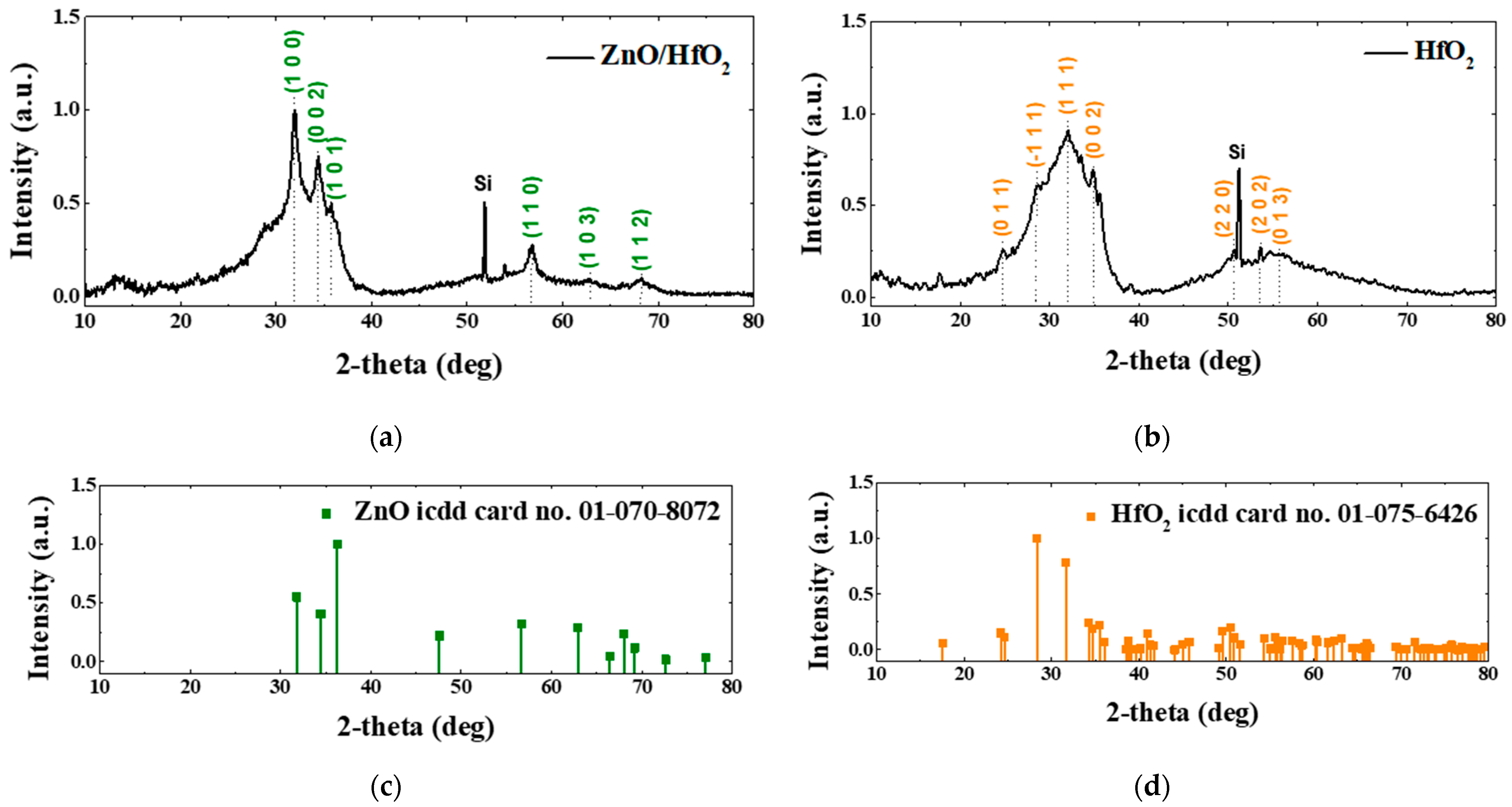
3.1. XRD Analysis of the ZnO/HfO2 Layer

The analysis of XRD is conducted using the 2-theta method. The XRD spectrum of the ZnO, used in the fabricated RRAM, is shown in Figure 2a. Compared to the ZnO ICDD card (no. 01-070-8072) in Figure 2c, the peaks at (100), (002), (101), (101), (110), (103), and (112) are observed. The ZnO exhibits a hexagonal wurtzite crystal structure. Regarding the XRD of the HfO2 layer shown in Figure 2b, when compared with the ICDD card (no. 01-075-6426) in Figure 2d, the peaks at (011), (-111), (111), (002), (220), (202), and (013) are identified. The HfO2 exhibits a crystalline structure, with monoclinic and orthorhombic phases [19]. The average grain size of each layer, calculated using Scherrer’s equation [20], is 10.9 nm for ZnO and 1.55 nm for the HfO2 layer.

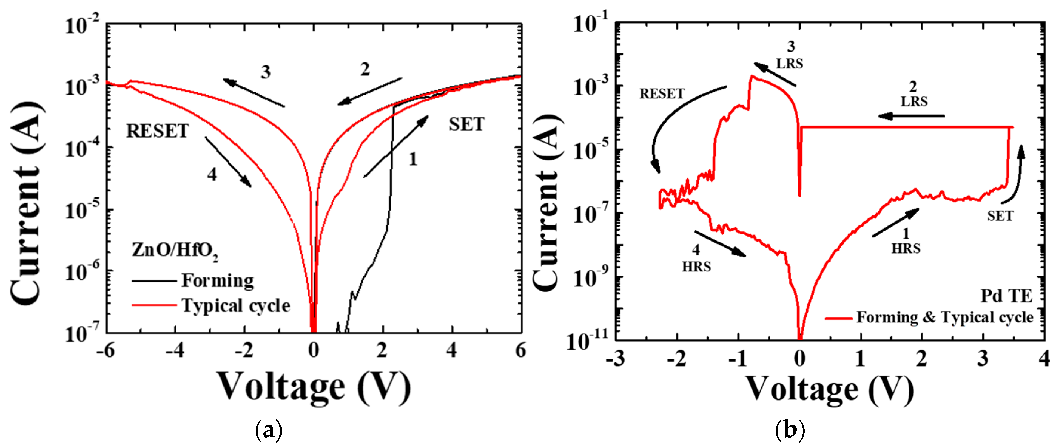
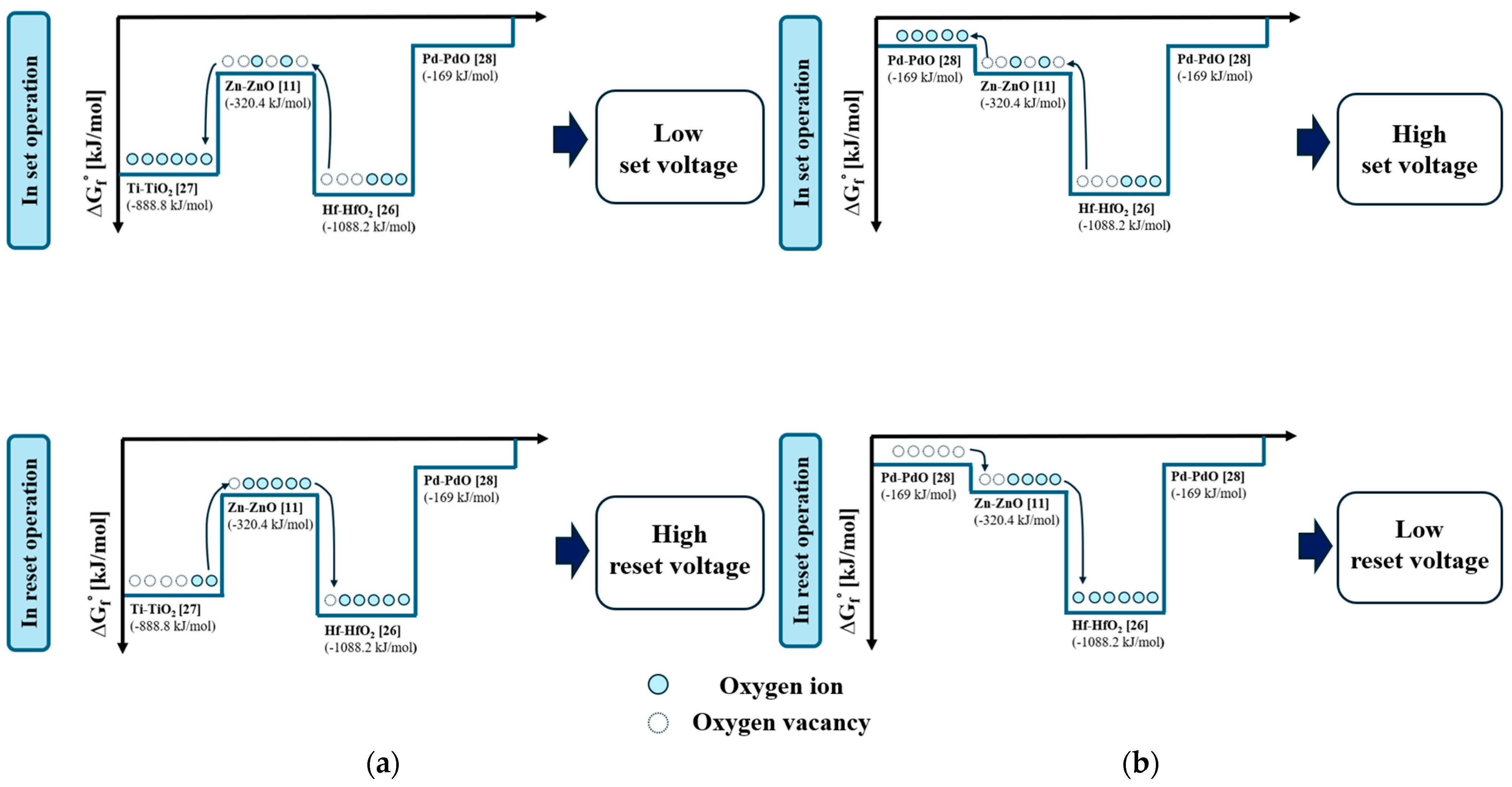
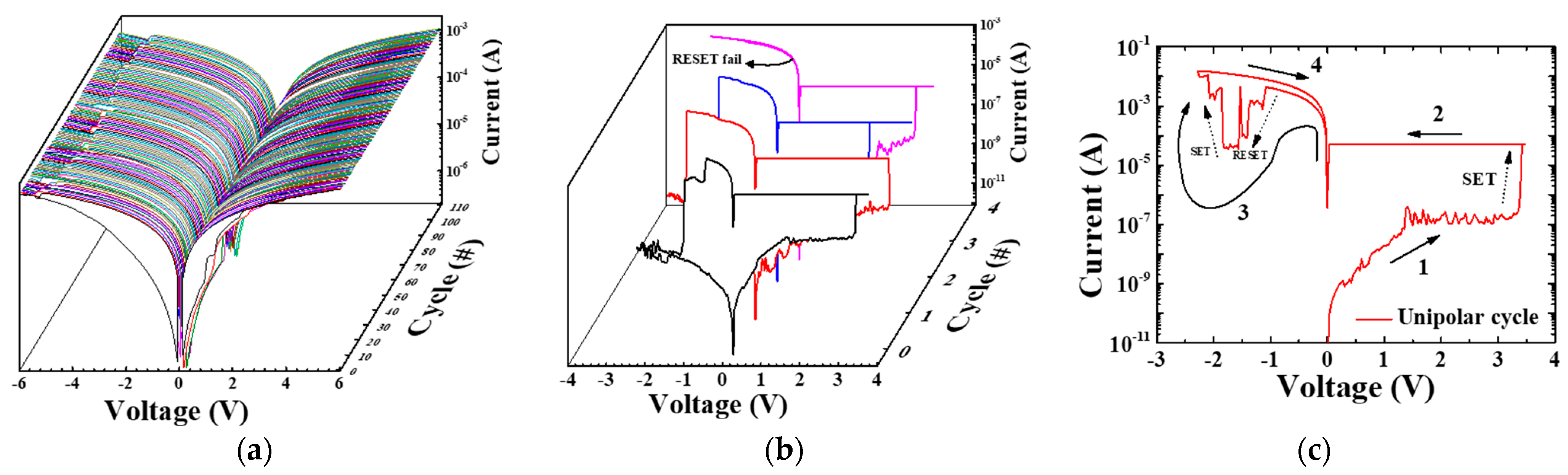
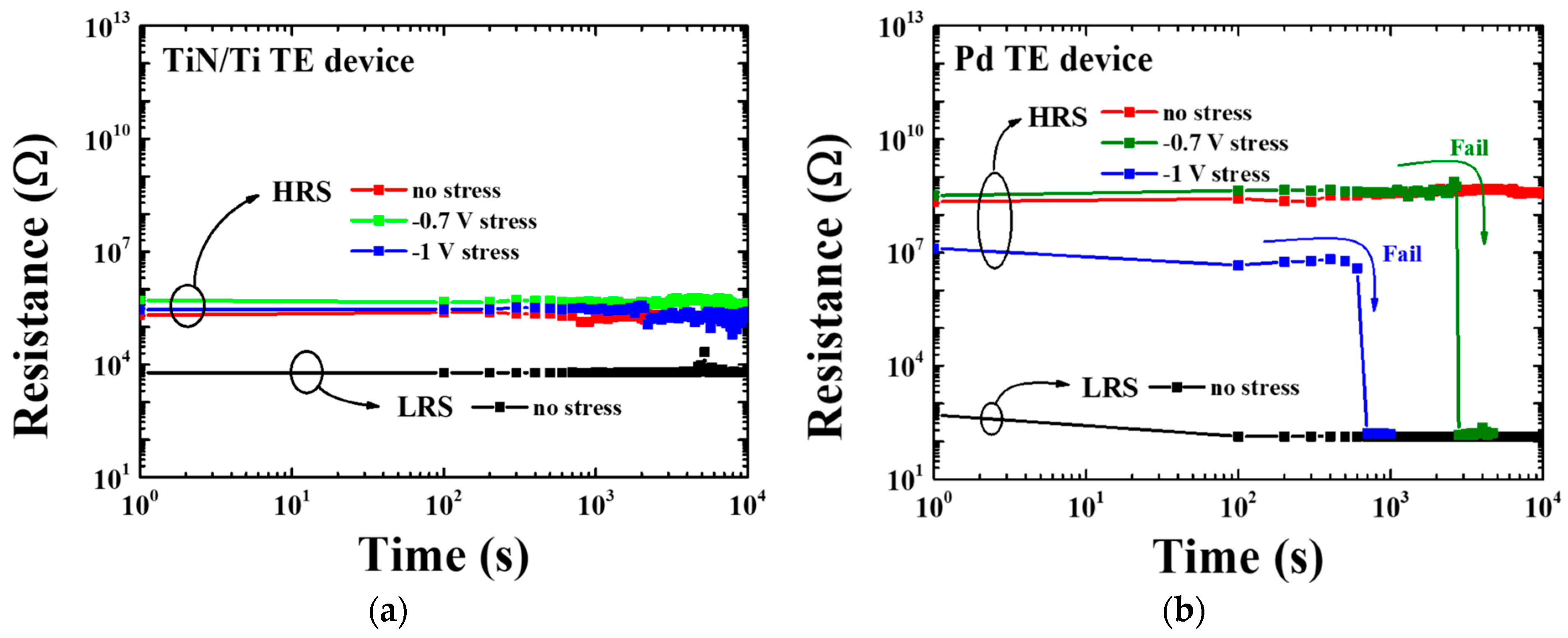
3.2. Electrical Properties of the TiN/Ti TE and Pd TE Device

Figure 3a displays the I–V curve of the TiN/Ti TE RRAM device, showing bipolar switching characteristics. The set voltage, which transitions the device from a high resistance state (HRS) to a low resistance state (LRS), ranges from 1.1 V to 2 V. The reset voltage, at approximately −5.1 V, transitions the device from LRS back to HRS. Additionally, the high oxygen reactivity of the TiN/Ti TE is attributed to an increase in oxygen vacancies, resulting in a relatively low resistance value in HRS. This leads to an increase in the leakage current and a decrease in the on/off ratio. In the case of single oxide layer devices, such as ZnO [21] and HfO2 [22] with Ti TE, similar results are observed, with the resistance value in HRS being close to 105 Ω. Furthermore, the TiN/Ti TE device maintains stable HRS below −6 V. Therefore, the TiN/Ti TE device shows stable bipolar switching in the ZnO/HfO2 RRAM with the TiN/Ti TE. In the case of the device featuring Pd TE, the I–V curve also exhibits bipolar switching behavior, as shown by the arrow sequence in Figure 3b. The set voltage is fixed at 3.5 V, and the reset voltage varies from −1.2 to −2.5 V, with the compliance current set at 50 μA. The Pd TE device, which has lower oxygen affinity, exhibits a higher resistance value in HRS compared to that of the TiN/Ti TE device. This is because the leakage current is reduced due to the small oxygen vacancy in the oxide [23].
To estimate the oxygen movement during the set and reset operation in the fabricated RRAM, the standard Gibbs free energy of formation (∆Gf°) is generally used [24,25]. The ∆Gf° value for materials used in the TiN/Ti TE device is shown in Figure 4a and for the Pd TE device in Figure 4b. From a thermodynamic perspective, based on ∆Gf° theory, HfO2, with the lowest value of −1088.2 kJ/mol [26], forms stable oxygen bonds in the device. Thus, the main switching layer, where resistance change occurs, is HfO2 for both devices. In the device, ZnO, with a value of −320 kJ/mol [11], acts as a buffer layer, providing oxygen ions or states of oxygen vacancy to other layers. When analyzing the impact of TE for both devices, the ∆Gf° of TEs becomes crucial. In the TiN/Ti TE device, ZnO supplies oxygen ions to TiO2, which has a low ∆Gf° value of −888.8 kJ/mol [27], thereby generating many states of oxygen vacancies in ZnO. The oxygen ions of HfO2 can easily move to ZnO, leading to the formation of filaments. This process requires lower energy for the formation of filaments, resulting in a lower set voltage. However, when a negative voltage is applied to TE, oxygen ions are forced to move to BE. Filling the generated oxygen vacancies in ZnO and HfO2 necessitates significant energy; thus, a higher reset voltage is required. In this process, TiO2, which exhibits a high irreversibility, does not return all oxygen, causing a significant flow of leakage current in the HRS. In contrast, in the Pd TE device, Pd has a ∆Gf° value of −169 kJ/mol [28], inhibiting the movement of oxygen ions in ZnO to the Pd and preventing the generation of states of oxygen vacancy in ZnO. Generating sufficient oxygen vacancies requires more energy, leading to a higher set voltage. Conversely, the low ∆Gf° value of Pd suggests a low irreversibility, making it relatively easier to fill oxygen vacancies. Thus, a lower reset voltage is needed. Wei Zhang et al. [29] also reported the same phenomenon when comparing the ZnO/HfO2 stack and the HfO2/ZnO stack with either Ti or Pt TE.
For the cycling test in the TiN/Ti TE device, the bipolar switching is maintained over 110 cycles, as depicted in Figure 5a. In the cycling test for the Pd TE device, depicted in Figure 5b, reset failure occurs after three cycles. This is caused in the Pd TE device by the unexpected unipolar switching under negative bias, as indicated by the arrow sequence in Figure 5c. This behavior is typical of unipolar switching, resulting from inert TE [30,31].
To examine the stress stability of the device, resistance measurements are conducted, depending on temperatures and voltage stress. When tested at a read voltage (Vread) of 0.5 V, the TiN/Ti TE device demonstrates stable HRS at 25 °C, 85 °C, 140 °C, and 150 °C, as shown in Figure 6a. However, the Pd TE device in Figure 6b exhibits failure after 6 × 10³ s at 150 °C. This is because the high temperature accelerates the diffusion of oxygen ions, thus reducing the stability of the HRS. It also suggests that the small number of filaments in the Pd device makes it more susceptible, probabilistically, to transitioning to the LRS due to diffusion. In the voltage stress test, the TiN/Ti TE device endures up to 104 s under negative voltage stress, depicted in Figure 7a. In contrast, the Pd TE device fails after 7 × 10² s at −0.7 V, and after 2 × 10³ s at −1 V, as shown in Figure 7b. The current induced by voltage stress within the oxide layer increases the temperature, leading to changes in the filaments and ultimately degrading stability. This phenomenon indicates that Pd devices are more susceptible to Joule heating, resulting in unstable unipolar operation. Conversely, TiN/Ti TE devices demonstrate better stability and reliability and are less sensitive to temperature fluctuations. This shows that TiN/Ti TE can maintain stable bipolar switching.
Considering the previous result, the switching mechanism is suggested for the TE. In ZnO/HfO2 bilayer RRAMs, filament formation and dissolution are dependent on the oxygen affinity of the TE. In structures with inert Pd metals for both BE and TE, as shown in Figure 8a, the stability of the filaments decreases due to the Joule heating effect. Also, the HRS of the Pd device is vulnerable to Joule heating when the negative bias is applied for a long period of time. Compared with the operational characteristics of the previously fabricated Pd TE device, this device exhibits lower stability, as observed in the mechanism shown in Figure 8a. Using a TiN/Ti TE with high oxygen affinity, as shown in Figure 8b, enables the formation of a stable filament and ensures stable operation. Therefore, the TiN/Ti TE device demonstrates relatively higher stability.

4. Conclusions

The ZnO/HfO2 bilayer RRAM devices using TiN/Ti TE and Pd TE are analyzed to evaluated their switching properties. The I–V curve indicates that the device with TiN/Ti TE exhibits a lower set voltage and a higher reset voltage. In contrast, the device with Pd TE demonstrates a higher set voltage and a lower reset voltage. This difference is due to the Gibbs free energy of the formation (∆Gf°) of TE, which influences the amount of energy required for oxygen movement, resulting in changes to the operating voltage. Additionally, cycling tests and retention measurements in Pd TE devices show low stability, which potentially leads to worse performance. This instability can be attributed to the effect of TE, which accelerates Joule heating and results in unipolar switching. To guarantee stable bipolar switching, the oxygen affinity of the material for TE should be considered. Overall, the choice of electrode material significantly affects the stability and performance of bilayer oxide RRAM devices.

Author Contributions

Methodology, formal analysis, investigation, conceptualization, validation, and writing—original draft preparation, S.-Y.K.; methodology and investigation, W.-S.K.; methodology and investigation, J.-H.B.; methodology and investigation, D.-Y.L.; funding acquisition and resource, H.-D.L.; writing—review and editing, supervision, funding acquisition, and project administration, G.-W.L. All authors have read and agreed to the published version of the manuscript.

Funding

This work was supported by research fund of Chungnam National University.

Data Availability Statement

No new data were created or analyzed in this study. Data sharing is not applicable to this article.

Conflicts of Interest

The authors declare no conflicts of interest.

References

  1. Lv, Z.; Wang, Y.; Chen, J.; Wang, J.; Zhou, Y.; Han, S.-T. Semiconductor quantum dots for memories and neuromorphic computing systems. Chem. Rev. 2020, 120, 3941–4006. [Google Scholar] [CrossRef] [PubMed]
  2. Lv, Z.; Xing, X.; Huang, S.; Wang, Y.; Chen, Z.; Gong, Y.; Zhou, Y.; Han, S.-T. Self-assembling crystalline peptide microrod for neuromorphic function implementation. Matter 2021, 4, 1702–1719. [Google Scholar] [CrossRef]
  3. Gao, Z.; Wang, Y.; Lv, Z.; Xie, P.; Xu, Z.-X.; Luo, M.; Zhang, Y.; Huang, S.; Zhou, K.; Zhang, G. Ferroelectric coupling for dual-mode non-filamentary memristors. Appl. Phys. Rev. 2022, 9, 021417. [Google Scholar] [CrossRef]
  4. Woo, J.; Moon, K.; Song, J.; Lee, S.; Kwak, M.; Park, J.; Hwang, H. Improved synaptic behavior under identical pulses using AlOx/HfO2 bilayer RRAM array for neuromorphic systems. IEEE Electron Device Lett. 2016, 37, 994–997. [Google Scholar] [CrossRef]
  5. Yu, S.; Wu, Y.; Chai, Y.; Provine, J.; Wong, H.-S.P. Characterization of switching parameters and multilevel capability in HfOx/AlOx bi-layer RRAM devices. In Proceedings of the 2011 International Symposium on VLSI Technology, Systems and Applications, Hsinchu, Taiwan, 25–27 April 2011; pp. 1–2. [Google Scholar]
  6. Chang, C.-F.; Chen, J.-Y.; Huang, G.-M.; Lin, T.-Y.; Tai, K.-L.; Huang, C.-Y.; Yeh, P.-H.; Wu, W.-W. Revealing conducting filament evolution in low power and high reliability Fe3O4/Ta2O5 bilayer RRAM. Nano Energy 2018, 53, 871–879. [Google Scholar] [CrossRef]
  7. Sadaf, S.M.; Liu, X.; Son, M.; Park, S.; Choudhury, S.H.; Cha, E.; Siddik, M.; Shin, J.; Hwang, H. Highly uniform and reliable resistance switching properties in bilayer WOx/NbOx RRAM devices. Phys. Status Solidi (A) 2012, 209, 1179–1183. [Google Scholar] [CrossRef]
  8. Chou, C.-T.; Hudec, B.; Hsu, C.-W.; Lai, W.-L.; Chang, C.-C.; Hou, T.-H. Crossbar array of selector-less TaOx/TiO2 bilayer RRAM. Microelectron. Reliab. 2015, 55, 2220–2223. [Google Scholar] [CrossRef]
  9. Zou, L.; Shao, J.; Bao, D. Enhanced resistive switching performance in bilayer Pt/TiO2/Co3O4/Pt memory device. Mater. Res. Express 2021, 8, 016404. [Google Scholar] [CrossRef]
  10. Wu, S.-J.; Wang, F.; Zhang, Z.-C.; Li, Y.; Han, Y.-M.; Yang, Z.-C.; Zhao, J.-S.; Zhang, K.-L. High uniformity and forming-free ZnO-based transparent RRAM with HfOx inserting layer. Chin. Phys. B 2018, 27, 087701. [Google Scholar] [CrossRef]
  11. Jain, N.; Sharma, S.K.; Kumawat, R.; Jain, P.K.; Kumar, D.; Vyas, R. Resistive switching, endurance and retention properties of ZnO/HfO2 bilayer heterostructure memory device. Micro Nanostruct. 2022, 169, 207366. [Google Scholar] [CrossRef]
  12. Hsieh, W.-K.; Lam, K.-T.; Chang, S.-J. Bipolar Ni/ZnO/HfO2/Ni RRAM with multilevel characteristic by different reset bias. Mater. Sci. Semicond. Process. 2015, 35, 30–33. [Google Scholar] [CrossRef]
  13. Ielmini, D.; Nardi, F.; Cagli, C. Universal reset characteristics of unipolar and bipolar metal-oxide RRAM. IEEE Trans. Electron Devices 2011, 58, 3246–3253. [Google Scholar] [CrossRef]
  14. Yu, S.; Wong, H.-S.P. A phenomenological model for the reset mechanism of metal oxide RRAM. IEEE Electron Device Lett. 2010, 31, 1455–1457. [Google Scholar] [CrossRef]
  15. Lee, H.D.; Magyari-Köpe, B.; Nishi, Y. Model of metallic filament formation and rupture in NiO for unipolar switching. Phys. Rev. B 2010, 81, 193202. [Google Scholar] [CrossRef]
  16. Wong, H.-S.P.; Lee, H.-Y.; Yu, S.; Chen, Y.-S.; Wu, Y.; Chen, P.-S.; Lee, B.; Chen, F.T.; Tsai, M.-J. Metal–oxide RRAM. Proc. IEEE 2012, 100, 1951–1970. [Google Scholar] [CrossRef]
  17. Zhou, P.; Yin, M.; Wan, H.; Lu, H.; Tang, T.; Lin, Y. Role of TaON interface for CuxO resistive switching memory based on a combined model. Appl. Phys. Lett. 2009, 94, 053510. [Google Scholar] [CrossRef]
  18. Uenuma, M.; Ishikawa, Y.; Uraoka, Y. Joule heating effect in nonpolar and bipolar resistive random access memory. Appl. Phys. Lett. 2015, 107, 073503. [Google Scholar] [CrossRef]
  19. Lee, T.; Ahn, J.; Oh, J.; Kim, Y.; Kim, Y.-B.; Choi, D.-K.; Jung, J. Characterization of Ultra-Thin HfO2 Gate Oxide Prepared by Using Atomic Layer Deposition. J.-Korean Phys. Soc. 2003, 42, 272–275. [Google Scholar]
  20. Cullity, B.D. Elements of X-ray Diffraction; Addison-Wesley Publishing: Boston, MA, USA, 1956. [Google Scholar]
  21. Bature, U.I.; Nawi, I.M.; Khir, M.H.M.; Zahoor, F.; Hashwan, S.S.B.; Algamili, A.S.; Abbas, H. Analysis of thermodynamic resistive switching in ZnO-based RRAM device. Phys. Scr. 2023, 98, 035020. [Google Scholar] [CrossRef]
  22. Traoré, B.; Xue, K.-H.; Vianello, E.; Molas, G.; Blaise, P.; De Salvo, B.; Padovani, A.; Pirrotta, O.; Larcher, L.; Fonseca, L. Investigation of the role of electrodes on the retention performance of HfOx based RRAM cells by experiments, atomistic simulations and device physical modeling. In Proceedings of the 2013 IEEE International Reliability Physics Symposium (IRPS), Monterey, CA, USA, 14–18 April 2013; pp. 5E.2.1–5E.2.6. [Google Scholar]
  23. Lin, C.-Y.; Wu, C.-Y.; Wu, C.-Y.; Lee, T.-C.; Yang, F.-L.; Hu, C.; Tseng, T.-Y. Effect of top electrode material on resistive switching properties of ZrO2 film memory devices. IEEE Electron Device Lett. 2007, 28, 366–368. [Google Scholar] [CrossRef]
  24. Ismail, M.; Rahmani, M.K.; Khan, S.A.; Choi, J.; Hussain, F.; Batool, Z.; Rana, A.M.; Lee, J.; Cho, H.; Kim, S. Effects of Gibbs free energy difference and oxygen vacancies distribution in a bilayer ZnO/ZrO2 structure for applications to bipolar resistive switching. Appl. Surf. Sci. 2019, 498, 143833. [Google Scholar] [CrossRef]
  25. Hsu, C.-C.; Sun, J.-K.; Tsao, C.-C.; Chuang, P.-Y. Effects of Gibbs free energy of interfacial metal oxide on resistive switching characteristics of solution-processed HfOx films. Phys. B Condens. Matter 2017, 519, 21–25. [Google Scholar] [CrossRef]
  26. Birks, N.; Meier, G.H.; Pettit, F.S. Introduction to the High Temperature Oxidation of Metals; Cambridge University Press: Cambridge, UK, 2006. [Google Scholar]
  27. Wang, X.P.; Chen, Y.Y.; Pantisano, L.; Goux, L.; Jurczak, M.; Groeseneken, G.; Wouters, D. Effect of anodic interface layers on the unipolar switching of HfO2-based resistive RAM. In Proceedings of the 2010 International Symposium on VLSI Technology, System and Application, Hsinchu, Taiwan, 26–28 April 2010; pp. 140–141. [Google Scholar]
  28. Nell, J.; O’Neill, H.S.C. Gibbs free energy of formation and heat capacity of PdO: A new calibration of the Pd PdO buffer to high temperatures and pressures. Geochim. Cosmochim. Acta 1996, 60, 2487–2493. [Google Scholar] [CrossRef]
  29. Zhang, W.; Guo, Z.; Dai, Y.; Lei, J.; Wang, J.; Hu, F. Effects of stacking sequence and top electrode configuration on switching behaviors in ZnO-HfO2 hybrid resistive memories. Ceram. Int. 2023, 49, 35973–35981. [Google Scholar] [CrossRef]
  30. Chen, J.-Y.; Hsin, C.-L.; Huang, C.-W.; Chiu, C.-H.; Huang, Y.-T.; Lin, S.-J.; Wu, W.-W.; Chen, L.-J. Dynamic evolution of conducting nanofilament in resistive switching memories. Nano Lett. 2013, 13, 3671–3677. [Google Scholar] [CrossRef]
  31. Kurnia, F.; Liu, C.; Jung, C.; Lee, B. The evolution of conducting filaments in forming-free resistive switching Pt/TaOx/Pt structures. Appl. Phys. Lett. 2013, 102, 152902. [Google Scholar] [CrossRef]
Figure 1. The schematic of (a) the TiN/Ti TE device, (b) the Pd TE device, and (c) the optical microscopic image of the fabricated device.
Electronicmat 05 00006 g001
Figure 2. X-ray diffraction (XRD) analysis of (a) the ZnO/HfO2 layer and (b) the HfO2 layer. The ICDD card data of (c) ZnO and (d) HfO2.
Electronicmat 05 00006 g002
Figure 3. The bipolar switching characteristic of (a) the TiN/Ti TE device and (b) the Pd TE device.
Electronicmat 05 00006 g003
Figure 4. The standard Gibbs free energy of formation (∆Gf°) and oxygen ion movement of (a) the TiN/Ti TE device and (b) the Pd TE device (based on the ideal operational scenario, without the diffusion).
Electronicmat 05 00006 g004
Figure 5. The cycling tests for (a) the TiN/Ti TE device and (b) the Pd TE device, showing (c) the unexpected unipolar switching characteristic of the Pd TE device under negative bias.
Electronicmat 05 00006 g005
Figure 6. Resistance measurement results with Vread = 0.5 V under different temperatures in the (a) TiN/Ti TE and (b) Pd TE devices.
Electronicmat 05 00006 g006
Figure 7. Resistance measurement results with Vread = 0.5 V under different voltage stress in the (a) TiN/Ti TE and (b) Pd TE device.
Electronicmat 05 00006 g007
Figure 8. The operation mechanism and switching characteristics depend on the TE: (a) the Pd TE device and (b) the TiN/Ti TE device.
Electronicmat 05 00006 g008
Disclaimer/Publisher’s Note: The statements, opinions and data contained in all publications are solely those of the individual author(s) and contributor(s) and not of MDPI and/or the editor(s). MDPI and/or the editor(s) disclaim responsibility for any injury to people or property resulting from any ideas, methods, instructions or products referred to in the content.

