Article

Measurement of Dielectric Properties of Thin Materials for Radomes Using Waveguide Cavities

by
Tayla Dahms
1,*,
Douglas B. Hayman
2,
Bahare Mohamadzade
2 and
Stephanie L. Smith
2
1
College of Science and Engineering, James Cook University, Douglas, QLD 4814, Australia
2
CSIRO Space and Astronomy, Marsfield, NSW 2122, Australia
*
Author to whom correspondence should be addressed.
Telecom 2024, 5(3), 706-722; https://doi.org/10.3390/telecom5030035
Submission received: 5 June 2024 / Revised: 11 July 2024 / Accepted: 23 July 2024 / Published: 1 August 2024

Abstract

:
We present waveguide cavity measurements used to evaluate several thin materials for use in radomes. In addition to the data on the materials, we show how these measurements can be performed with common laboratory equipment and simple calculations. We sought an approach that allowed candidate materials to be readily evaluated to deal with formerly selected materials becoming unavailable or cost-prohibitive. We used lengths of standard waveguide (WR650 and WR137 here) with readily manufactured irises and a vector network analyzer (Keysight N5225B here). To select the iris size and determine the limits of the simplifications in the equations used, we employed a full-wave 3D electromagnetic simulator (CST Microwave Studio). The equations required to calculate the dielectric properties of samples and their contribution to the equivalent system noise temperature from unloaded and loaded resonant frequencies and Q factors are shown. While these formulations can be found elsewhere, we did not find these assembled as conveniently in other studies in the literature. We also show that orienting the sample down the length of the cavity allows for higher-order modes to be fully utilized. We did not find this straightforward adaptation of the common cross-guide orientation in other works. Overall, the results allowed us to recommend three fabrics for use at the frequencies tested (1.7 and 5.6 GHz). The complete process is outlined to assist others in performing these measurements themselves.

1. Introduction

Radomes are weatherproof structures that protect enclosed antennas and their systems from external environmental factors such as debris, rain, ice, wind, and dust [1]. The shape of a radome generally depends upon the application, with geodesic, spherical, and planar being common [1]. The material and structure of a radome are designed to minimize adverse effects on an antenna’s electromagnetic (EM) performance. Negative impacts of a radome on antenna operation can include insertion loss (IL), increased sidelobe levels of the antenna radiation pattern, increased depolarization of the radiation pattern, and boresight error (BSE) [1]. The IL effects can be further divided into the loss in the gain, the ripple in the gain, and the increase in noise due to radiation from a lossy radome.
Permittivity ( ϵ ) is a particularly important property for dielectrics used as radomes. It is generally expressed as a complex parameter and as the relative permittivity ( ϵ r ) for a material under test at a certain orientation within an electric field [2]. The real part of this complex permittivity ( ϵ r ) is called the dielectric constant. The loss tangent is another important characteristic to measure for materials, as it is the ratio of the imaginary part to the real part of the relative permittivity, and is expressed as follows:
tan δ = ϵ r ϵ r
It is important to note that the permittivity can be dependent upon temperature and frequency. As such, differing frequencies propagating through the material can experience different values of permittivity. High values of permittivity increase the losses from reflected waves [1,2]. Similarly, the loss tangent affects the amount of loss and noise in a system. As such, it is important that materials with low-loss tangents are used for radomes [3]. Therefore, dielectrics with low permittivity and loss tangents at various frequencies are the most appropriate for radome structures.
The precise measurement of these materials to identify their permittivity can be challenging. Permittivity measurements can be performed on many types and forms of materials—bulk, thin, solid, liquid, ceramic, plastic, and even organics [2,4]. These different materials have various applications, including capacitors, transformers, switches, cabling, reactors, and cooling systems [5]. Each of these materials can have multiple measurement processes available, each with its own advantages and disadvantages, dependent upon the type of material and application. All methods mentioned in this paper utilize the modes of propagating waves through the material. This paper focuses on transverse electric (TE) and transverse magnetic (TM) modes, as shown in Figure 1 [6,7]. Mode degeneracy is when multiple modes have the same propagation coefficient, causing overlap when viewing the modal signals. This can make it difficult to single out the chosen mode peak [8].
Choosing an appropriate method for measurement can be difficult and depends upon various factors. The authors in [2] provide a simple set of questions to help determine which measurement method is the best. These questions include the material category (bulk or thin), whether the sample under test requires non-destructive means of measurement, the type of frequency band (broad or narrow required, the measurement accuracy required (high or low), and what the dielectric losses are expected to be (high or low). These questions help to narrow down the requirements of the measurement and determine the most accurate method for not only the frequency range but also the thickness of the material [2].
Rhode and Schwartz provide a comprehensive overview of the most popular methods for this measurement process in [4]. They outline four prevalent methods: transmission/reflection line, open-ended coaxial probe, free-space, and resonant (cavity) [4]. Table 1, adapted from [4], summarizes the types of materials that would be most appropriate for each popular method of measurement. It also details which mode is assumed to perform these measurements. As dielectric property measurement is a long-standing topic, several recent works can provide some context for the different processes available for various types of materials [9,10,11,12,13].
We focused on the application of radomes, which, in our area of interest, require thin, flexible, inelastic materials. Also called ‘skin’ materials, as their thickness can be down to the micrometer, these materials include a variety of types, including flexible fabrics [2,4].
There exist some permittivity measurement methods specific to testing skin materials. As with all permittivity measuring methods, they also depend upon the frequency range required for operation. Figure 2 summarizes prevalent methods of permittivity measurement across the EM spectrum [2]. This figure shows how a few measurement methods can be used across a majority of the frequency spectrum, such as capacitors, open coax probes, and transmission lines. On the other hand, most other methods can be used at various narrow bands at the higher end of the spectrum.
Traditionally, thin films are measured with a capacitor setup. This requires a miniature microwave probe, where a thin dielectric film is deposited on a metal layer and then a top electrode layer. This allows for a one-port reflection measurement to be taken. The reflection coefficient is then measured from the incident waves and converted to impedance, from which the loss tangent can then be extracted [14]. However, in [14], the authors acknowledge that this does not create a perfect plate capacitance. Therefore, further complex calculations are required to account for the various losses across the multi-layered plates [14].
Our initial motivation for this research was to create a material database detailing relevant characteristics for use as radome covers, specifically for large phased arrays working around 1 to 6 GHz. Therefore, our research intended to begin at 1 GHz and increase in frequency as measurement methods became available to our lab. As such, according to Figure 2, a type of resonator would be the best method for this frequency area of interest.
Dielectric resonators are used to hold a sample within a simple cavity so an electric field can be applied to it. Identifying the correct mode and measuring the resonant frequency and Q-factor before and after the sample is placed within the resonator allows the calculation of the permittivity to be completed. Q-factors are the frequency-to-bandwidth ratios of the cavity for the mode in question [15]. This type of resonator measurement is present in previous research, such as [2,16,17]. However, although these resonators are generally simple shapes, like cylinders, they are still specific devices created for permittivity measurement. As such, they may not be available within most labs that have not previously conducted research into resonance and characteristic measurements of materials. Therefore, a much more accessible method is needed.
Waveguide cavities are also a popular method for measuring microwave frequencies. This method requires a waveguide cavity for the chosen operation band of frequency, a network analyzer, the sample material cut to the size of the cavity, and foam to hold the sample in place within the cavity. The same method used with the resonator method is then followed to obtain the S21 parameter of the cavity with and without the sample present. This difference is then used to calculate the permittivity and loss tangent. This method, used in [18,19], is easily accessible for most microwave and RF labs that may be interested in determining these material characteristics themselves. The biggest downfall of this method is that it is destructive, in that samples must be made to fit within the cavity. For example, flexible fabrics need to be cut to size to fit within the waveguide for testing. Therefore, some wastage is present for this method. However, the waveguide method is accurate at lower loss values, making it appealing for many applications [20]. Due to the accessibility of the equipment required, it is also considered more economically viable, especially compared with the capacitance method, which can require specific microwave and network analyzer probes.
Overall, there are various techniques available in the literature for measuring thin films at multiple frequencies. However, our goal with this paper was to provide detailed steps for an accurate measurement method that can be performed with simple equipment available in most RF labs. This method also utilizes a new setup, where the material sample is never fully placed within a null of the electric field, which means that multiple modes are available for useful measurement. This then allows for dielectric property measurements to be more accessible while also acknowledging how simple and cost-effective this process can be. Unlike other works on dielectric measurement, this paper provides comprehensive information, including a review of all dielectric measurement methods for different types of materials, factors for choosing the best method, theoretical details of the current measurement method, details of simulations, and all measurement factors and setup configuration for a vector network analyzer (VNA). This thorough approach was designed to help readers replicate the experimental process for their materials and understand the considerations for their own measurement setups. In addition, to the best of our knowledge, this is the only paper that covers the results from the measurement of several materials after proposing and explaining the method and simulation in detail, including pictures of the measurement setups. This is different from other papers that only cover the mathematical background of the model and theoretical materials.
The following Section 2 outlines the methods followed for this measurement process, while Section 3 outlines the simulated and measured results obtained using this method and discusses what these findings mean. Finally, the conclusions drawn from this research are summarized in Section 4.

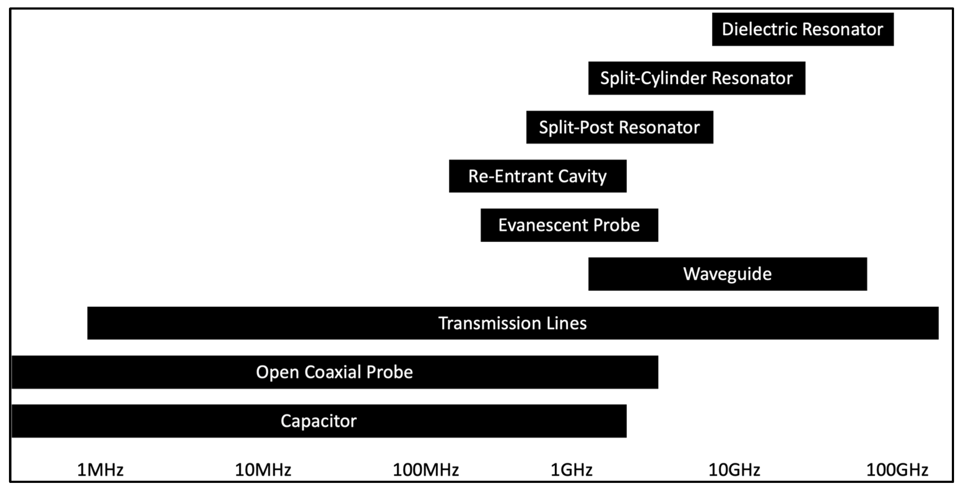
2. Theory and Materials

As mentioned in the Introduction section, one of the most common methods used for determining dielectric properties is the resonant cavity method. This involves placing the material under test within a waveguide cavity with shims (with irises in their center) on each end, identifying the resonant frequency, and then using that to calculate permittivity and loss tangent [9].
The relevant resonant frequencies, the dimensions of the waveguide cavity, and the mode numbers are used in Equation (2) to determine both TE and TM modes (noting that TM modes have m values greater than zero):
f = c 2 m a 2 + n b 2 + p l 2 ,
where f is the resonant frequency (Hz); c is the speed of light; m , n , and p are given by the chosen mode TEmnp or TMmnp; and a , b , and l are the width, height, and length of the waveguide cavity, as shown in Figure 3 and Figure 4 [15].
By determining multiple cutoff frequencies, various mode resonances can be observed within the cavity. The first eight propagating modes of a rectangular waveguide that are excited at the iris of the shim are TE10, TE30, TE12, TM12, TE50, TE32, TM32, and TE52 [22,23]. These modes are excited by a symmetrical iris when the electric field in the y direction has values of m odd and n even. A benefit of this measurement method is the ability to look at properties at higher frequencies that are outside the waveguide’s recommended frequency range.
The orientation of the material under test within the waveguide cavity is also an important factor. Generally, test materials are placed within the x-y plane of the cavity, with the largest side of the sample facing each of the irises, as shown in Figure 5b. However, for the research discussed in this article, we placed our samples in the y-z plane of the cavity, as shown in Figure 5a. This was done so that the sample is exposed to the maximum integrated electric field for the TE10p modes and thus has the highest filling factor (Equation (9)). For p > 1 , the filling factor for the x-y case was zero for p , even as the sample sat in a null. This can be understood by observing the two modes in Figure 5 [21]. As we focused on the fundamental TE10 mode, we observed it travels along the length of the cavity (z-axis). For the first cavity mode of TE101, there was no null present in the electric field. However, for the second (TE102) and higher cavity modes, we observed the presence of a null where the electric field crossed the center of the z-axis. If the material under test was placed within this null, it would not be affected by the electric field, resulting in no useful measurements. Therefore, to ensure that we had multiple modes available for measurement, we avoided placing the sample within a null by placing it in the y-z plane.
To calculate the permittivity and loss tangent of a sample material using cavity resonance, specific equations are required. For simulations, different equations were used, as the foam holding the sample in place within the cavity was not simulated. These equations used for calculating real and imaginary permittivity and the loss tangent are shown in Equations (3)–(5) [20].
ϵ = ( f c f s ) 2 f s V C V s + 1 ,
ϵ = V C 4 V s 1 Q s 1 Q c ,
tan δ = ϵ ϵ ,
where the subscripts c and s represent the empty cavity and the cavity with the sample, respectively. The resonant frequency is represented by f , while Q is the Q-factor, and V C and V S represent the volume of the cavity and volume of the sample, respectively.
We also required certain equations to account for the loss of the foam that was used to hold the sample in place within the cavity. Therefore, Equations (5)–(10) were used for the actual measurement process. First, the real and imaginary parts of permittivity and loss tangent for the empty cavity and the filled cavity, which was filled with foam only, were calculated [20]. From there, the loss tangent and real and imaginary parts of the permittivity could be determined for the sample material (Equations (5)–(7)). Then, with Equations (9)–(11), we first found a filling factor based on the orientation of the sample in the cavity and then the real part of permittivity and the loss tangent were calculated. The real part of permittivity was found by assuming that the real part of permittivity was much larger than the imaginary part ( ϵ ϵ ). The permittivity and loss tangent were determined by treating the cavity as partially filled, as the sample material only partially filled the cavity [20]. These simplified equations rely on approximations dependent on the loss tangent being very low and the resonant mode amplitude being much higher than any other modes. They were sufficiently accurate for this application.
These equations are known as simplified equations, as they assume that the loss tangent is very low and the resonant mode is much greater than the other modes. However, they were sufficiently accurate for this research application.
ϵ 1 = f 0 f 1 2 ,
ϵ 1 = 1 Q 1 1 Q 0 f 0 f 1 f 0 f 1 2 ,
tan δ 1 = ϵ 1 ϵ 1 ,
C y z = 2 t a ,
ϵ 2 = ϵ 1 2 C f 1 f 2 f 2 + 1 ,
tan δ 2 = ϵ 1 2 ϵ 1 ϵ 2 C 1 Q 2 1 Q 1 + tan δ 1 ,
where subscript 0 represents an empty cavity, subscript 1 represents the cavity filled with only foam, and subscript 2 represents the cavity with both foam and the sample. As previously stated, C y z is the filling factor based on the orientation of the sample within the cavity, and a is the width of the cavity. The thickness of the sample is represented by t , and the various resonant frequencies are represented by f . The units of the parameters need only be consistent as all dimensions are ratios of the same physical quantities. The Q-factors are shown by Q , and C denotes whichever filling factor is being used.
Some cost-effective materials are available in the form of weatherproof canvas or similar fabrics. However, as these are not created specifically for radome applications, the dielectric properties of these materials are unknown. We initially ordered seven fabrics of various thicknesses, rigidity, and types from ExtremTextil in Germany [25]. These fabrics and their thicknesses are noted in Table 2, each with a shortened name for ease of reading throughout this report. The thicknesses of these materials were manually measured with digital calipers.
Some features of these fabrics are summarized in Table 3. These features are either important or useful for a radome fabric to ensure that the covered systems are protected from weather and/or debris. For example, a material being flame-retardant is not essential but is a useful feature. On the other hand, being water- and windproof is essential for a radome material. These features, alongside the loss tangent and permittivity values, assist with determining which materials could be appropriate options for radomes.
Therefore, in the following section, the simplified equations method is used to determine the unknown dielectric properties of the materials being investigated to establish their appropriateness for radome applications.

3. Results

3.1. Simulated Results

To confirm the accuracy of the simplified equations found in the literature, simulations of a waveguide cavity were performed in CST Studio Suite [24]. To begin this modeling, the cavity size had to be chosen. Due to the waveguide cavities available to us, a WR650 cavity and a WR137 cavity were chosen, with a length of 105 mm and 127 mm, respectively. A WR650 waveguide has a recommended frequency band of 1.15 to 1.72 GHz and a width and height of 165.1 mm and 82.55 mm, respectively [28]. A WR137 waveguide has a recommended frequency band of 5.85 to 8.20 GHz and a width and height of 34.85 mm and 15.8 mm, respectively [29]. By using Equation (2), many mode frequencies were calculated (p = 1, 2,..., 10) for the WR650 and WR137 cavities and then sorted by frequency (see Table 4 and Table 5 [30,31]). This allowed for an easier identification of the correct modes in both simulations and measurements, as mode overlap and degeneracy can occur when multiple modes are excited at similar or the same frequencies. This is observed with the frequencies displayed in Table 4 and Table 5, where there are multiple modes around 6 GHz for the WR650 cavity and 22 GHz for the WR137 cavity.
Next, the most appropriate diameter for the iris in the shims was determined. The smaller the iris, the weaker the coupling and the higher the Q-factor. The larger the iris, the higher the transmission coefficient, and hence the signal to noise on the measurement of center frequency and Q. The diameter of the iris was chosen to ensure that the Q-factor dropped significantly when the material sample was added to the cavity. Previous experience within our group was used to help determine that a radius of 6.1 mm (7.4% of the narrow wall), and thus a diameter of 12.2 mm, would work best for the WR650 cavity. For the WR137 cavity, a shim iris diameter of 7.2 mm was chosen.
These diameters were then used in the simulation model in CST Studio Suite [24]. The s-parameters were checked to ensure the model performed as expected, with clear resonant peaks and no discontinuities. To check the accuracy of Equations (3)–(5), multiple models of a WR650 cavity were simulated in CST with loss tangents of 0.1, 0.05, 0.01, 0.005, and 0.001 and permittivity values of 1.5, 2.2, and 2.9 corresponding to the range of values we were interested in for skin materials in radome applications. The S21 data from these numerous simulations were then processed in the same way as the experimental data to assist in determining whether these simplified equations were accurate and reliable.
The results obtained from these simulations are displayed in Table 6 for the WR650 cavity and in Table 7 for the WR137 cavity.
In Table 6, by comparing the simulated permittivity ( ϵ r s i m ) and loss tangent ( tan δ s i m )) values to the calculated permittivity ( ϵ r ) and loss tangent ( tan δ ) values, we case see that there is little error between the two. Even for the lower loss tangent values, we see quite good agreement between the simulated and calculated values. By calculating the percentage error, we can further confirm this agreement. The results in Table 5 show that we obtained a permittivity error of less than 1% and a loss tangent error of less than 24%. We observed similar findings for the WR137 cavity.
Table 7 shows that there was little error between the simulated and calculated permittivity values and loss tangents for a WR137 cavity with a shim iris of 7.2 mm diameter. The percentage error for each of these properties also supports this argument. We obtained a permittivity error of less than 2% and a loss tangent error of less than 27%. These results show that Equations (3)–(5) were accurate and reliable and that the y-z orientation of a material is possible. Therefore, with the verification of the accuracy of these simplified equations, we can begin our measurement process for the chosen materials. We can then apply these formulas to calculate the unknown dielectric properties of our candidate materials. This will then allow us to identify the suitability of these non-radome fabrics for radome applications and even further testing and verification at different frequencies.

3.2. Measurement Setup

3.2.1. Material Preparation

For the cavity measurements, two pairs of shims were manufactured out of aluminum with the irises in the center of each shim and the bolt holes to the WR650 and WR137 standards. The foam to hold the sample in place was also cut to fit each cavity. This foam was split into two pieces so a sample piece of material could be held between the blocks of foam within the y-z plane. The pieces of fabric were manually cut to the size of the cavity with a ruler and scissors.

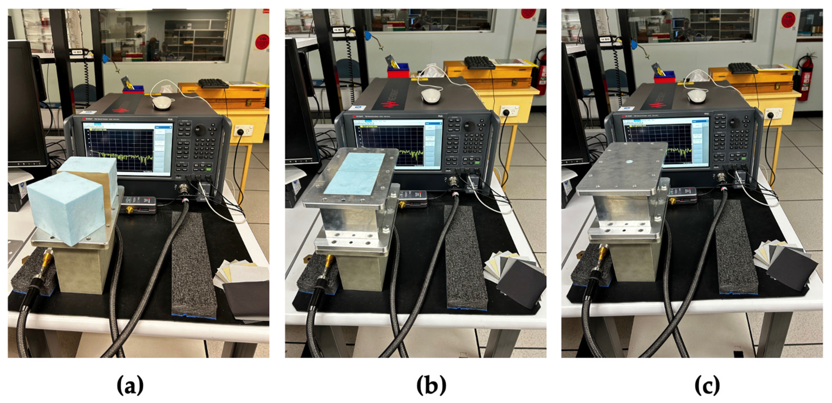
3.2.2. Network Analyzer Setup

The measurement steps are as follows:
  • Connect waveguide adapters to the empty cavity with shims on either side;
  • Save resonant peak data for the empty cavity;
  • Disconnect adapters from the cavity;
  • Place foam blocks within the cavity;
  • Reconnect shims and adapters;
  • Save resonant peak data for the cavity filled with foam;
  • Disconnect adapters from the cavity;
  • Remove foam blocks from the cavity;
  • Place the sample within foam blocks;
  • Carefully place foam blocks and the sample within the cavity;
  • Reconnect adapters to the cavity;
  • Save resonant peak data for the cavity filled with foam and the sample material;
  • Repeat steps 9 to 12 for each material sample.
Figure 6 displays the motions of adding a sample to the cavity before the second waveguide adapter is connected. The first waveguide adapter is connected to the network analyzer, and then the shim is placed on the adapter, with the cavity connected next. The material under test is placed between the two foam blocks, which are then carefully placed within the cavity, avoiding the movement of the sample between the blocks. The second shim is then placed on the other side of the cavity before the second waveguide adapter is connected to the cavity. The final setup for this experiment is shown in Figure 7, where the cavity is connected to the network analyzer.
Once the waveguide cavity was connected to the network analyzer, the resonant peaks were observed across a large frequency range. To ensure smooth peaks, averaging on the network analyzer was used to allow the waveform to settle. Increasing the averaging on the network analyzer can ensure smoother waveforms. However, this can increase the amount of time needed for this measurement process to wait for the averaging to complete. Through this observation, it was decided that the dominant mode (TE101) resonant peak would be used throughout the measurement process for WR650. This was done as it had the cleanest peak, identified at about 1.6 GHz, and thus would provide the most accurate results, as there was less chance of mode degeneracy. A similar process was followed to determine that the TE103 mode would be the most appropriate to observe for the WR137 cavity, as it is the most isolated resonant peak for this cavity at 5.575 GHz.

3.2.3. Collecting Data

Initially, the empty waveguide cavity was connected to the network analyzer, sandwiched between two shims. The resonant peak of the dominant mode was identified at about 1.6 GHz for the WR650 cavity and 5.575 GHz for the WR137 cavity. To be able to obtain the half-power bandwidth of this peak, data points 3 dB below the peak were needed. Therefore, we manually zoomed into the resonant peak on the network analyzer to ensure that there would be a high enough frequency resolution for this bandwidth calculation. This resonant peak was then saved in an s2p file for evaluation in a Jupyter Notebook [30].
This process was repeated with the addition of only foam within the cavity and then foam and each material sample within the cavity (as outlined previously).
It was observed that some materials immediately did not meet the requirements of a radome application. They either had loss tangents of greater than 0.05 or permittivity values of greater than 3. These values, especially at this low frequency as permittivity and loss tangent tend to increase with increased frequency, tell us that these materials would create too much loss within the system. This is especially important for our intended application of radio astronomy, as any loss, even 0.1 dB, can add unwanted noise [32]. Therefore, results were only collected for five materials, including the two reference materials. Once the resonant peaks were obtained for each material under test, the data within the s2p files were able to be imported into the Jupyter Notebook for further analysis [30].
Using the scikit-rf package for Python, the resonant peak data were extracted from each of the s2p files [33]. The data from the simulated cavities were also exported from CST Studio Suite in s2p files. Each of the resonant peaks was then replotted within the notebook to ensure that the peak was clean and to easily extract the bandwidth for each of the Q-factors [30,31,34]. Example resonant peaks for the WR650 cavity are shown in Figure 8. The simulated plots have different S21 values than the experimental plots, as our models were simulated in ideal conditions, with the material of the shims and cavity set as pure aluminum, while our actual materials were not. The frequency spans were also different as we zoomed into the experimental peak on the network analyzer to ensure that the clear peak was observed, with large amounts of data available for use.

3.3. Measured Results

Once the appropriate data, such as frequencies and bandwidths, were extracted, Equations (6)–(11) were then used to calculate the permittivity and loss tangent of each material under test within the WR650 and WR137 cavities [30,31,33,34]. These results are summarized in Table 8.
The results for these two cavities initially tell us that reference radome materials had permittivity values of about 2.6 and 2.9 but very low loss tangents of less than 0.002 for lower frequencies and less than 0.02 at higher frequencies. This highlights the importance of knowing the permittivity and having a low loss for radome applications. These results also showcase the viability of three materials within the materials purchased for this experiment. N-Shell, 3-LL, and 2-LL demonstrate much lower permittivity values than the reference materials, with approximated permittivity of 1.4, 2, and 1.9, respectively.
The equivalent noise temperature added by these materials can be calculated using Equation (12).
T n = T p h y s 1 L l i n e a r ,
where T n is the noise temperature in Kelvin, T p h y s is the physical temperature of the room where the measurements were obtained, and l o s s is the absorption losses of S21. These losses were determined using the previously calculated properties of each material, including the permittivity ( ϵ r ), loss tangent ( tan δ ), material thickness ( d ) in meters, and frequency ( f ) in gigahertz (Equations (13) and (14)) [21].
L l i n e a r = 10 8.686 α d 10 ,
α = π f μ 0 ϵ 0 ϵ r tan δ ,
where μ 0 is the dielectric constant (4π × 10−7 H/m), and ϵ 0 is the electric constant (8.854 × 10⁻¹² F/m).
Using Equations (12)–(14), we determined the following noise contributions due to the losses for each material, as shown in Table 8. We can observe noise temperature contributions of less than 0.4 K at 5.575 GHz and 0.1 K at 1.65 GHz. The fabric with the best results, other than the two reference materials, was N-Shell, with noise contributions of 0.0236 K at the lower frequency and only 0.1169 at the higher frequency. These results are quite promising for the investigated fabrics.
We can also observe that there were some slight differences in measured values between the two cavities. This is unexpected and could be due to the various factors discussed in the following section, Section 3.4.
Therefore, we can conclude that our results for these materials are accurate enough to determine which materials would be most suitable for further testing as a radome. We suggest that N-Shell would be the most appropriate due to its low permittivity of 1.4 and relatively low loss tangent of less than 0.01. It would also be worth further investigating 3-LL and 2-LL as they also displayed similarly low values for permittivity and loss tangent across the approximate 1 to 6 GHz range.

3.4. Measurement Factors

Despite these positive results, there are some factors that require consideration when following this type of measurement method. A major factor is the room temperature and its impact on the resonant cavity. Fluctuations in temperature can affect the data obtained through the network analyzer. This is especially observable if measurements are conducted on particularly warm days or performed over multiple days without remeasuring the foam-only case, which should be avoided wherever possible. Another possible solution is to perform measurements in a temperature-controlled environment to ensure that external factors are consistent. Measuring the cavity with only foam after each sample measurement is also another way to ensure that consistent measurements are performed. The network analyzer settings are also important, as the number of points can impact the accuracy of the data obtained from the resonant peak plot. Increasing the power of the network analyzer can assist in producing a better signal-to-noise ratio and, hence, a higher Q-factor. This can be especially important for smaller shim irises and smaller waveguide cavities, which tend to provide, overall, more consistent and accurate results. The averaging of the signal can also be useful to ensure that an accurate peak is observed. Other factors that may have negative impacts also include foam distortion and mode degeneracy. Due to the tight fit required for the foam blocks within the waveguide cavity, inserting and removing them did result in slight indentations, which could have small effects on the consistency of the measurements. This removal and insertion process also caused some foam dust to be created. We found that this dust needed to be carefully cleaned from the waveguide mating surfaces each time the cavity was assembled to avoid lowering the Q-factors. Finally, mode degeneracy was observed during this experiment, specifically at some of the modes past the dominant mode. This degeneracy, or overlapping of modes, results in overlapping peaks, which can mean that accurate resonant peaks were not able to be identified at these other modes. Also, as this measurement technique utilizes Equations (6)–(11), it must be acknowledged that these are simplified equations. Therefore, some factors affecting permittivity and loss are not included.
Further measurements are required at various higher frequencies to identify if these materials are suitable beyond the range covered here. Also, the measurement of these fabrics in different environments such as hot, cold, or wet, could also help to find any impacts radomes made of these materials may have on their antennas.
With this further testing, we hope to create a database of materials that describes their features and performance at various frequencies and in multiple environments. The goal is to ease the process of finding appropriate materials when designing radomes and antennas, as well as identify cost-effective fabrics for these applications.

4. Conclusions

Permittivity, loss tangents, and noise results were obtained for widely available fabrics with the intention to use them as radomes within the frequency range of about 1 to 6 GHz. Good agreement between full wave simulation and the simplified equations gave confidence in the application of those equations to the measurements. These measured results, performed with WR650 and WR137 waveguide resonant cavities and shim iris diameters of 12.2 mm and 7.2 mm, respectively, showed encouraging outcomes for three fabrics. This was observed through the comparison with two reference materials previously used for antenna array radomes. These results confirm that cost-effective, widely available materials could be appropriate in radome applications. Factors that impacted measurements were also identified and discussed, with possible solutions provided. Further testing of these materials within different environments and at higher frequencies will further identify their appropriate usage. The orientation of these materials in the y-z plane of the cavity will allow for measurements to be obtained at higher frequencies using higher-order modes with the same setup we used in this article. This exemplifies how this newly proposed orientation can make this commonly used method even easier for numerous measurements.

Author Contributions

Conceptualization, D.B.H. and B.M.; methodology, D.B.H. and B.M.; software, D.B.H., B.M. and T.D.; validation, T.D. and B.M.; formal analysis, T.D.; investigation, T.D. and B.M.; resources, D.B.H. and B.M.; data curation, T.D.; writing—original draft preparation, T.D.; writing—review and editing, T.D., D.B.H., B.M. and S.L.S.; visualization, T.D.; supervision, D.B.H. and S.L.S.; project administration, B.M..; funding acquisition, T.D. and S.L.S. All authors have read and agreed to the published version of the manuscript.

Funding

This research was funded by the Australian Government Research Training Program Scholarship and CSIRO PhD Top-Up Scholarship.

Data Availability Statement

Data will be made available upon reasonable request to the corresponding author.

Conflicts of Interest

The authors declare no conflicts of interest.

References

  1. Shavit, R. Radome Electromagnetic Theory and Design; Wiley: Hoboken, NJ, USA, 2018. [Google Scholar]
  2. Baker-Jarvis, J.; Janezic, M.D.; Degroot, D.C. High-frequency dielectric measurements. IEEE Instrum. Meas. Mag. 2010, 13, 24–31. [Google Scholar] [CrossRef]
  3. Kumar, C.; Mohammed, H.U.R.; Peake, G. mmWave Radar Radome Design Guide. 2021. Available online: https://www.ti.com/lit/an/swra705/swra705.pdf?ts=1708569361624&ref_url=https%253A%252F%252Fdev.ti.com%252F (accessed on 1 May 2024).
  4. Yaw, K.C. Measurement of Dielectric Material Properties—Application Note; RAC0607-0019_1_4E; Rohde & Schwarz Report: Munich, Germany, 2012. [Google Scholar]
  5. Elmelin Marketing. What Are the Types of Dielectric Material? Available online: https://elmelin.com/what-are-the-types-of-dielectric-material/ (accessed on 1 May 2024).
  6. Kuphaldt, T.R. Lessons in Electric Circuits, 6th ed.; 2021. Available online: https://www.ibiblio.org/kuphaldt/electricCircuits/AC/AC_14.html (accessed on 1 May 2024).
  7. Poole, I. Waveguide Modes. Electronics Notes. Available online: https://www.electronics-notes.com/articles/antennas-propagation/rf-feeders-transmission-lines/waveguide-modes-te-tm-tem.php (accessed on 1 May 2024).
  8. Wells, C.G.; Ball, J.A.R. Mode-matching analysis of a shielded rectangular dielectric-rod waveguide. IEEE Trans. Microw. Theory Tech. 2005, 53, 3169–3177. [Google Scholar] [CrossRef]
  9. Meda, V.; Raghavan, V. An Overview of Dielectric Properties Measuring Techniques. Can. Biosyst. Eng./Le Genie Des. Biosyst. Au Can. 2005, 47, 15–30. [Google Scholar]
  10. Chung, B.-K. Dielectric constant measurement for thin material at microwave frequencies. Prog. Electromagn. Res. 2007, 75, 239–252. [Google Scholar] [CrossRef]
  11. Park, S.; Yoon, S.; Ahn, Y. Dielectric constant measurements of thin films and liquids using terahertz metamaterials. RSC Adv. 2016, 6, 69381–69386. [Google Scholar] [CrossRef]
  12. Krraoui, H.; Mejri, F.; Aguili, T. Dielectric constant measurement of materials by a microwave technique: Application to the characterization of vegetation leaves. J. Electromagn. Waves Appl. 2016, 30, 1643–1660. [Google Scholar] [CrossRef]
  13. Zahedi, A.; Boroumand, F.A.; Aliakbrian, H. Analytical transmission line model for complex dielectric constant measurement of thin substrates using T-resonator method. IET Microw. Antennas Propag. 2020, 14, 2027–2034. [Google Scholar] [CrossRef]
  14. Ma, Z.; Becker, A.J.; Polakos, P.; Huggins, H.; Pastalan, J.; Wu, H.; Watts, K.; Wong, Y.H.; Mankiewich, P. RF measurement technique for characterizing thin dielectric films. IEEE Trans. Electron Devices 1998, 45, 1811–1816. [Google Scholar] [CrossRef]
  15. Cheng, D.K. Field and Wave Electromagnetics, 2nd ed.; Addison-Wesley Publishing Company: Boston, MA, USA, 1983. [Google Scholar]
  16. Easton, C.D.; Jacob, M.V.; Krupka, J. Non-destructive complex permittivity measurement of low permittivity thin film materials. Meas. Sci. Technol. 2007, 18, 2869. [Google Scholar] [CrossRef]
  17. Krupka, J. Precise measurements of the complex permittivity of dielectric materials at microwave frequencies. Mater. Chem. Phys. 2003, 79, 195–198. [Google Scholar] [CrossRef]
  18. Chung, B.K. A convenient method for complex permittivity measurement of thin materials at microwave frequencies. J. Phys. D Appl. Phys. 2006, 39, 1926. [Google Scholar] [CrossRef]
  19. Hasar, U.C.; Simsek, O. An accurate complex permittivity method for thin dielectric materials. Prog. Electromagn. Res. 2009, 91, 123–138. [Google Scholar] [CrossRef]
  20. Dube, D.C.; Lanagan, M.T.; Kim, J.H.; Jang, S.J. Dielectric measurements on substrate materials at microwave frequencies using a cavity perturbation technique. J. Appl. Phys. 1988, 63, 2466–2468. [Google Scholar] [CrossRef]
  21. Marcuvitz, N. Waveguide Handbook; McGraw-Hill: New York, NY, USA, 1951. [Google Scholar]
  22. Chew, W.C. Lectures on Theory of Microwave and Optical Waveguides; University of Illinois Urbana-Champaign: Champaign, IL, USA.
  23. Pozar, D.M. Microwave Engineering; Wiley: Hoboken, NJ, USA, 2011. [Google Scholar]
  24. Dassault Systemes. “CST Studio Suite”. Available online: https://www.3ds.com/products/simulia/cst-studio-suite (accessed on 1 May 2024).
  25. extremtextil. Available online: https://www.extremtextil.de/en/ (accessed on 1 May 2024).
  26. Swift Supplies Online. Available online: https://www.swiftsupplies.com.au/ (accessed on 1 May 2024).
  27. Ripstop by the Roll. Available online: https://ripstopbytheroll.com/ (accessed on 1 May 2024).
  28. everythingRF. WR650|WG6|R14-Rectangular Waveguide Size. everythingRF. Available online: https://www.everythingrf.com/tech-resources/waveguides-sizes/wr650 (accessed on 1 May 2024).
  29. everythingRF. WR137|WG14|R70-Rectangular Waveguide Size. everythingRF. Available online: https://www.everythingrf.com/tech-resources/waveguides-sizes/wr137 (accessed on 1 May 2024).
  30. Kluyver, T.; Ragan-Kelley, B.; Pérez, F.; Granger, B.; Bussonnier, M.; Frederic, J.; Kelley, K.; Hamrick, J.; Grout, J.; Corlay, S.; et al. Jupyter Notebooks—A publishing format for reproducible computational workflows. In Positioning and Power in Academic Publishing: Players, Agents and Agendas; IOS Press: Amsterdam, The Netherlands, 2016; pp. 87–90. [Google Scholar]
  31. Harris, C.R.; Millman, K.J.; Van Der Walt, S.J.; Gommers, R.; Virtanen, P.; Cournapeau, D.; Wieser, E.; Taylor, J.; Berg, S.; Smith, N.J.; et al. Array programming with NumPy. Nature 2020, 585, 357–362. [Google Scholar] [CrossRef] [PubMed]
  32. Kozakoff, D.J. Analysis of Radome-Enclosed Antennas, 2nd ed.; Artech House Antennas and Propagation Series; Artech House: Boston, MA, USA, 2009. [Google Scholar]
  33. Arsenovic, A.; Hillairet, J.; Anderson, J.; Forstén, H.; Rieß, V.; Eller, M.; Sauber, N.; Weikle, R.; Barnhart, W.; Forstmayr, F. scikit-rf: An Open Source Python Package for Microwave Network Creation, Analysis, and Calibration [Speaker’s Corner]. IEEE Microw. Mag. 2022, 23, 98–105. [Google Scholar] [CrossRef]
  34. Hunter, J.D. Matplotlib: A 2D Graphics Environment. Comput. Sci. Eng. 2007, 9, 90–95. [Google Scholar] [CrossRef]
Figure 1. TE and TM mode field orientations, where the E-field is depicted in blue and the H-field in red [6] (reproduced with permission from T.R. Kuphaldt, Lessons in Electric Circuits; 2021).
Telecom 05 00035 g001
Figure 2. Permittivity measurement methods most appropriate for various bands of the frequency spectrum [2].
Telecom 05 00035 g002
Figure 3. Coordinate system and dimensions of a general rectangular waveguide [15].
Telecom 05 00035 g003
Figure 4. Rectangular waveguide cavity with the variations in electric field for resonant modes TE101 (p = 1) and TE102 (p = 2) [21].
Telecom 05 00035 g004
Figure 5. Material under test orientations: (a) sample in y-z (used in this work); (b) sample in x-y plane (traditionally used) [24].
Telecom 05 00035 g005
Figure 6. Various stages of setup for measuring dielectric properties of materials: (a) material under test within the foam blocks; (b) foam and sample within WR650 waveguide cavity; (c) shims on either side of the WR650 waveguide cavity before the final waveguide adapter is attached.
Telecom 05 00035 g006
Figure 7. Final WR650 waveguide cavity and network analyzer setup to measure the dielectric properties of possible radome materials. Multiple resonant peaks are displayed on the network analyzer in the background.
Telecom 05 00035 g007
Figure 8. Examples of normalized simulated and experimental resonant peak of dominant TE101 mode for WR650 cavity: (a) empty; (b) with only foam; (c) with foam and PTFE Fabric sample [30,31,34].
Telecom 05 00035 g008
Table 1. Summary of popular permittivity measurement methods with the types of material that can be measured and the modes that are assumed [4].
Measurement MethodMaterial TypesAssumed Mode
Transmission/reflection lineCoaxial line, waveguidesFundamental
Open-ended coaxial probeLiquids, biological specimen, semi-solidsTEM, TE
Resonant cavityHigh temperatures, large/flat solids, gas, hot liquidsTM, TE
Free-spaceRod-shaped solids, waveguides, liquidsTEM
Table 2. Materials being investigated, their shortened names for ease of reading, and their thicknesses [25,26,27].
Material NameSimple NameThickness
(mm)
PTFE Coated Glass Fabric * [26]PTFE Fabric0.15
Dyneema composite fabric hybrid * [27]Dyneema0.1
Polyester, PU-Coated, impregnated, flame retardant, 240 g/sqm [25]Polyester0.19
Ecopak EPX70 RS, Ripstop, recycling-backpack-laminate, 171 g/sqm [25]Ecopak0.15
Etaproof 200, waterproof cotton, 200 g/sqm, 2nd Choice [25]Etaproof0.27
Cordura, 500 den, coated [25]Cordura0.36
N-Shell, z-liner pocket lining, 70 g/sqm [25]N-Shell0.3
3-layer-laminate, robust, mini-ripstop, 170 g/sqm [25]3-LL0.3
2-layer-laminate, soft, slightly elastic, 105 g/sqm [25]2-LL0.2
* Reference materials that have been used as radomes in previous projects.
Table 3. Features of the fabrics to assess their applicability as radomes [25,26,27].
MaterialFeatures
Flame-RetardantWaterproofWindproofAbrasion
Resistant
Inelastic
PTFE Fabric *Telecom 05 00035 i001Telecom 05 00035 i001Telecom 05 00035 i001Telecom 05 00035 i001Telecom 05 00035 i001
Dyneema * Telecom 05 00035 i001Telecom 05 00035 i001Telecom 05 00035 i001Telecom 05 00035 i001
PolyesterTelecom 05 00035 i001Telecom 05 00035 i001Telecom 05 00035 i001 Telecom 05 00035 i001
Ecopak Telecom 05 00035 i001Telecom 05 00035 i001Telecom 05 00035 i001Telecom 05 00035 i001
Etaproof Telecom 05 00035 i001Telecom 05 00035 i001 Telecom 05 00035 i001
Cordura Telecom 05 00035 i001Telecom 05 00035 i001Telecom 05 00035 i001Telecom 05 00035 i001
N-Shell Telecom 05 00035 i001Telecom 05 00035 i001 Telecom 05 00035 i001
3-LL Telecom 05 00035 i001Telecom 05 00035 i001 Telecom 05 00035 i001
2-LL Telecom 05 00035 i001Telecom 05 00035 i001
* Reference materials that have been used as radomes in previous projects.
Table 4. The resonant cavity frequencies for a WR650 waveguide cavity of 105 mm length sorted by frequency.
WR650 (Length = 105 mm)
ModeFrequency (GHz)ModeFrequency (GHz)ModeFrequency (GHz)ModeFrequency (GHz)
TE1011.69TE3236.25TE3068.99TE32812.30
TE1023.00TM3236.25TE5259.21TM32812.30
TE3013.08TE5036.25TE1269.35TE50812.30
TE3023.95TE3046.33TM1269.35TE52812.82
TE1214.01TE5226.48TE3269.70TE10912.89
TM1214.01TE1246.83TM3269.70TE30913.14
TE1034.38TM1246.83TE5069.70TE12913.39
TE1224.71TE1057.20TE10710.04TM12913.39
TM1224.71TE5237.23TE52610.36TE32913.64
TE3214.76TE3247.30TE30710.36TM32913.64
TM3214.76TM3247.30TE12710.68TE50913.64
TE5014.76TE5047.30TM12710.68TE52914.11
TE3035.08TE3057.65TE32710.98TE101014.31
TE3225.37TE1258.07TM32710.98TE301014.54
TM3225.37TM1258.07TE50710.98TE121014.77
TE5025.37TE5248.15TE10811.46TM121014.77
TE1235.69TE3258.47TE52711.57TE321014.99
TM1235.69TM3258.47TE30811.75TM321014.99
TE1045.79TE5058.47TE12812.03TE501014.99
TE5215.99TE1068.62TM12812.03TE521015.42
Table 5. The resonant cavity frequencies for a WR137 waveguide cavity of 127 mm length sorted by frequency.
WR137 (Length = 127 mm)
ModeFrequency (GHz)ModeFrequency (GHz)ModeFrequency (GHz)ModeFrequency (GHz)
TE1014.46TE12119.50TE12922.18TM32624.03
TE1024.91TM12119.50TM12922.18TE32724.41
TE1035.58TE12219.61TE50522.32TM32724.41
TE1046.39TM12219.61TE50622.66TE501024.55
TE1057.31TE12319.79TE121022.77TE32824.83
TE1068.29TM12319.79TM121022.77TM32824.83
TE1079.32TE12420.03TE32122.99TE32925.30
TE10810.38TM12420.03TM32122.99TM32925.30
TE10911.47TE12520.35TE50723.05TE321025.82
TE101012.57TM12520.35TE32223.08TM321025.82
TE30112.97TE12620.72TM32223.08TE52128.72
TE30213.13TM12620.72TE32323.23TE52228.80
TE30313.39TE12721.15TM32323.23TE52328.92
TE30413.75TM12721.15TE32423.44TE52429.09
TE30514.20TE50121.55TM32423.44TE52529.30
TE30614.73TE12821.64TE50823.50TE52629.56
TE30715.33TM12821.64TE32523.71TE52729.87
TE30816.00TE50221.65TM32523.71TE52830.21
TE30916.73TE50321.81TE50924.00TE52930.60
TE301017.50TE50422.03TE32624.03TE521031.03
Table 6. Results from simulated WR650 waveguide cavities in CST Studio Suite. It displays various simulated permittivity and loss tangents alongside the calculated permittivity and loss tangent values. It also displays the errors for each characteristic.
Simulated
Permittivity
( ϵ r s i m )
Simulated
Loss Tangent ( tan δ s i m )
Calculated
Permittivity
( ϵ r )
Calculated
Loss Tangent ( tan δ )
Permittivity
Error (%)
Loss Tangent
Error (%)
1.50.11.49640.11420.2414.2
0.051.48880.05380.757.6
0.011.4920.01060.536
0.0051.49290.00510.472
0.0011.49450.00110.3710
2.20.12.1950.11440.2314.4
0.052.19440.05150.253
0.012.1950.01010.231
0.0052.19440.00610.2522
0.0012.19660.00110.1510
2.90.12.88880.12320.3923.2
0.052.90840.05890.2917.8
0.012.89820.01110.0611
0.0052.90350.00570.1214
0.0012.90270.00110.0910
Table 7. Results from simulated WR137 waveguide cavities in CST Studio Suite. It displays various simulated permittivity and loss tangents alongside the calculated permittivity and loss tangent values. It also displays the errors for each characteristic.
Simulated
Permittivity
( ϵ r s i m )
Simulated
Loss Tangent ( tan δ s i m )
Calculated
Permittivity
( ϵ r )
Calculated
Loss Tangent ( tan δ )
Permittivity
Error (%)
Loss Tangent
Error (%)
1.50.11.47680.12161.5521.6
0.051.48840.05490.779.8
0.011.49420.01130.3913
0.0051.49260.00540.498
0.0011.49260.00080.4920
2.20.12.17940.11100.9411
0.052.18060.05440.888.8
0.012.18320.01170.7617
0.0052.18320.00480.764
0.0012.21050.001030.483
2.90.12.85460.11291.5712.9
0.052.84820.05351.797
0.012.85140.01261.6826
0.0052.84820.00541.798
0.0012.84490.00091.9010
Table 8. Summary of each material’s name, thickness, and calculated permittivity, loss tangent, and noise temperature for the five materials under test within WR650 and WR137 cavities for possible radome applications.
MaterialThickness (m)WR650 (Length = 105 mm)
TE101 (fc = 1.65 GHz)
WR137 (Length = 127 mm)
TE103 = (fc = 5.575 GHz)
PermittivityLoss TangentNoise (K)PermittivityLoss TangentNoise (K)
PTFE Fabric *0.000152.90.00090.00242.870.00440.0392
Dyneema *0.00012.60.00190.00322.580.01350.0760
N-Shell0.00031.40.00640.02361.40.00940.1169
3-LL0.00032.090.02250.10121.980.02440.3608
2-LL0.00021.870.02080.05901.850.02670.2545
* Reference materials that have been used as radomes in previous projects.
Disclaimer/Publisher’s Note: The statements, opinions and data contained in all publications are solely those of the individual author(s) and contributor(s) and not of MDPI and/or the editor(s). MDPI and/or the editor(s) disclaim responsibility for any injury to people or property resulting from any ideas, methods, instructions or products referred to in the content.

