Proceeding Paper

Optimization of the Geometry of a Microelectromechanical System Testing Device for SiO2—Polysilicon Interface Characterization †

1
Dipartimento di Ingegneria Civile e Ambientale, Politecnico di Milano, Piazza Leonardo da Vinci, 32, 20133 Milano, Italy
2
STMicroelectronics, 20007 Cornaredo, Italy
*
Author to whom correspondence should be addressed.
Presented at the 10th International Electronic Conference on Sensors and Applications (ECSA-10), 15–30 November 2023; Available online: https://ecsa-10.sciforum.net/.
Eng. Proc. 2023, 58(1), 82; https://doi.org/10.3390/ecsa-10-16033
Published: 15 November 2023

Abstract

:
Microelectromechanical systems (MEMSs) are small-scale devices that combine mechanical and electrical components made through microfabrication techniques. These devices have revolutionized numerous technological applications, owing to their miniaturization and versatile functionalities. However, the reliability of MEMS devices remains a critical concern, especially when operating in harsh conditions like high temperatures and humidities. The unknown behavior of their structural parts under cyclic loading conditions, possibly affected by microfabrication defects, poses challenges to ensuring their long-term performance. This research focuses on addressing the reliability problem by investigating fatigue-induced delamination in polysilicon-based MEMS structures, specifically at the interface between SiO2 and polysilicon. Dedicated test structures with piezoelectric actuation and sensing for closed-loop operation were designed, aiming to maximize stress in regions susceptible to delamination. By carefully designing these structures, a localized stress concentration is induced to facilitate the said delamination and help understand the underlying failure mechanism. The optimization was performed by taking advantage of finite element analyses, allowing a comprehensive analysis of the mechanical responses of the movable parts of the polysilicon MEMS under cyclic loading.

1. Introduction

In the realm of microelectromechanical systems (MEMSs), the fusion of miniaturized mechanical and electrical components through microfabrication techniques has spearheaded a technological revolution. These devices have demonstrated immense potential for multiple applications, driven by their compact form and multifaceted functionalities [1,2,3,4]. However, amid the proliferation of their application, the crucial concern of reliability looms large [2,5,6,7], particularly when they are exposed to challenging operational conditions such as high load cycles, elevated temperatures, and high humidities [8]. A thorough assessment of their mechanical reliability stands as a crucial requirement to propel the ongoing development of MEMSs.
The dominance of polycrystalline silicon in crafting MEMSs designed to sustain high-frequency oscillations is driven by its exceptional mechanical properties, outperforming many alternative materials. Despite its inherent brittleness and the absence of dislocation motion at temperatures below 900 °C, its operating conditions do not typically induce fatigue mechanisms [5,8]. Nevertheless, in some cases, MEMS devices exhibit heightened susceptibility to environmental factors that impact both the mechanical and electrical characteristics of the device. Paradoxically, fatigue stands as one of the critical failure mechanisms in such systems, highlighting the importance of thorough consideration and analysis of the mechanical properties of polysilicon [9,10,11,12,13,14,15]; see also [16,17].
An additional failure mode, likely to manifest under cyclic loading due to elevated interfacial stress levels and often in conjunction with fatigue, is delamination. This localized cracking-like failure mode typically occurs at the interface between silicon dioxide and polycrystalline silicon. The fatigue and delamination phenomena both lead to a progressive shift in resonance frequency, structural stiffness (also affected by uncertainties at the microscale; see [18,19,20,21,22]), and electrical resistance, thereby affecting the long-term reliability of these devices [9,23,24,25].
Effectively replicating fatigue failures through experimental tests requires the utilization of setups enabling relatively high-frequency testing, ideally in the range of kHz. Such high-frequency driving enables a significant number of cycles to be achieved within a reasonable timeframe, which is critical for an accurate fatigue analysis. In this context, on-chip tests emerge as the optimal choice, given their capability to operate over large frequency ranges [26].
By employing purpose-built test structures leveraging piezoelectric actuation and sensing for closed-loop operation, this research seeks to optimize the stress field within the movable structure of ad hoc-designed MEMS test structures. We take advantage of finite element analyses to enhance the stress concentrations at the interface between SiO2 and polysilicon in order to possibly induce fatigue-driven delamination. The optimization procedure is based on static analyses to obtain an idea of the best shape of the mechanical parts to induce a large stress concentration at the said interface, thus leading to the failure analysis in the experimental section to follow.

2. Materials and Methods

As anticipated, a polysilicon-based MEMS test structure was ad hoc designed to maximize the stress concentration, possibly leading to delamination-driven failure modes. The optimization of the geometry of the structure was made possible by the finite element software COMSOL Multiphysics®, through its MEMS module [27].
Figure 1 displays the initial geometry used for the optimization process, which is a bridge-like test structure actuated in bending mode. The main material layers are single-crystal silicon and silicon dioxide, on top of which the polycrystalline silicon movable structure is laid. In addition, four PZT-based patches are used for actuation and sensing, as highlighted in red in the figure. The shape optimization procedure was carried out by varying the length of the beam connecting the plate and the SiO2–polycrystalline silicon interface and also by allowing for the following constraints:
  • The failure-governing principal stress component at the interface should be as high as possible, ideally close to 1 GPa, in order to speed up the fatigue tests.
  • The stress field in the polysilicon layer should not exceed the one at the interface to avoid inducing brittle cracking in the latter region [28,29,30,31,32,33,34,35,36,37,38,39].
The numerical investigation includes two types of analysis (see Figure 2): (i) a stationary analysis performed on the entire structure and characterized by a coarse mesh optimized to achieve a trade-off between accuracy and computational cost requirements; (ii) a stationary analysis performed only on the region under study, namely on the central portion of the device, characterized by a finer mesh optimized to achieve accuracy in terms of the stress field. To take into account the non-linear geometric effects linked to the deformed configuration of the structure, a sufficiently high driving voltage is adopted in the first stationary analysis. Afterward, this solution is used as the starting configuration for the evaluation of the stress field using the finer mesh of the second analysis.
The mechanical properties of the main materials that make up the test structure are gathered in Table 1. The properties of single-crystal silicon in the <100> crystallographic direction are shown [40].

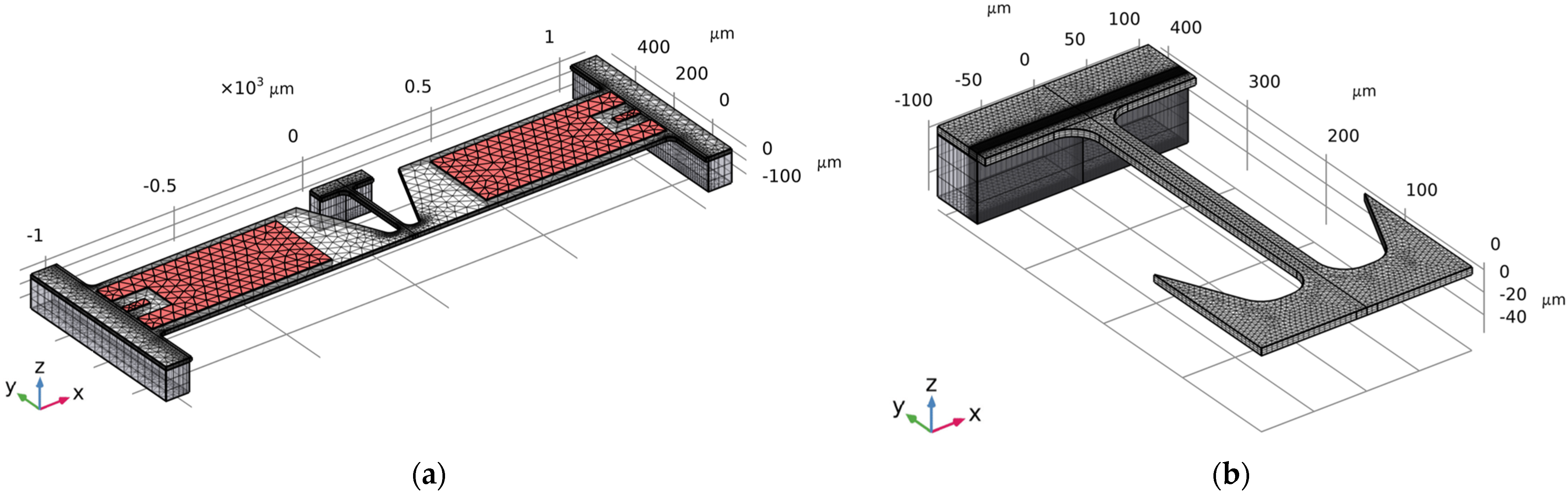
3. Results and Discussion

A series of stationary analyses were conducted for a beam length, L, ranging between 60 µm and 300 µm at a given applied driving voltage. Taking advantage of the 3-1 piezoelectric coupling mechanism of the PZT, an axial deformation of the beam is induced, leading to a bending-dominated structural deformation mode and, therefore, to displacements in the out-of-plane z-direction. With the structure being fully constrained at its two side ends, the load is transmitted through the beam and measured through the deflection at the center to also quantify the induced solution at the interface where the stress must be intensified.
The results of the local analyses featuring the finest mesh are depicted in Figure 3. It is shown that, as expected, for very high values of L, the structure becomes very compliant, as highlighted by the large deflection values attained, and the stress transmitted to the SiO2–polysilicon interface becomes very small if compared to the stress exhibited in the polysilicon layer, specifically along the rounded corners highlighted in red in the figure. As the beam length, L, decreases, the vertical displacement at the middle point decreases as well due to a stiffening of the structure, along with the principal stress in the rounded region. On the contrary, the stress at the SiO2–polysilicon interface keeps increasing until it reaches a maximum value of about 800 MPa, notably higher than the stress in the polysilicon, amounting to about 700 MPa. Afterward, the stress at the interface starts to drop due to the constrain joint at the center of the movable plate, which induces a stress redistribution throughout the entire structure.

4. Conclusions

In this study, a new design for a MEMS test structure based on piezoelectric actuation and sensing for closed-loop operation was reported. By means of finite element analyses, its geometry was optimized in order to maximize the stress at the SiO2–polysilicon interface, as a concentration can lead, in real-life situations, to delamination events. A maximum stress equivalent to about 800 MPa was attained, which resulted in being higher than the stress in the polysilicon to increase the probability of a localized crack-driven failure at such an interface and close to the target value of 1 GPa needed to speed up the fatigue tests.
These findings will be further developed by taking into consideration other geometric parameters in the optimization process that may lead to a higher stress intensification at the interface. The actual dynamic response of the structures to a sinusoidal, time-varying electric potential will also be assessed and compared to the outcome of an experimental study.

Author Contributions

Conceptualization, D.C., S.M., M.M. and G.F.; methodology, D.C.; software, D.C.; formal analysis, D.C., S.M., M.M. and G.F.; investigation, D.C., S.M., M.M. and G.F.; resources, D.C. and S.M.; data curation, D.C.; writing—original draft preparation, D.C.; writing—review and editing, S.M.; visualization, S.M.; supervision, S.M.; project administration, S.M.; funding acquisition, S.M. All authors have read and agreed to the published version of the manuscript.

Funding

The project was funded by STMicroelectronics under the Joint Research Platform STEAM, project Steam-P5 “Reliability of MEMS”.

Institutional Review Board Statement

Not applicable.

Informed Consent Statement

Not applicable.

Data Availability Statement

The data presented in this study are available on request from the corresponding author. The data are not publicly available due to some confidentiality issues.

Acknowledgments

The authors are indebted to Roberto Carminati, Carlo Valzasina, and Aldo Ghisi for a number of fruitful discussions in the early stages of the present study.

Conflicts of Interest

The authors declare no conflicts of interest.

References

  1. Frangi, A.; Cercignani, C.; Mukherjee, S.; Aluru, N. Advances in Multiphysics Simulation and Experimental Testing of Mems, 1st ed.; Imperial College Press: London, UK, 2008. [Google Scholar]
  2. Tsuchiya, T. Mechanical reliability of silicon microstructures. J. Micromech. Microeng. 2021, 32, 013003. [Google Scholar] [CrossRef]
  3. Younis, M.I. MEMS Linear and Nonlinear Statics and Dynamics, 1st ed.; Springer: New York, NY, USA, 2011. [Google Scholar]
  4. Gad-el-Hak, M.; Seemann, W. MEMS Handbook, 1st ed.; CRC Press: Boca Raton, FL, USA, 2002. [Google Scholar]
  5. Corigliano, A.; Ardito, R.; Comi, C.; Frangi, A.; Ghisi, A.; Mariani, S. Mechanics of Microsystems, 1st ed.; Wiley: Chichester, UK, 2018. [Google Scholar]
  6. Saleem, M.; Nawaz, H. A Systematic Review of Reliability Issues in RF-MEMS Switches. Micro Nanosyst. 2019, 11, 11–33. [Google Scholar] [CrossRef]
  7. Rajagopalan, J. Microelectromechanical Systems (MEMS)-Based Testing of Materials. In Handbook of Mechanics of Materials, 2nd ed.; Schmauder, S., Chen, C.S., Chawla, K., Chawla, N., Chen, W., Kagawa, Y., Eds.; Springer: Singapore, 2019; pp. 1955–1979. [Google Scholar]
  8. Bhalerao, K.; Soboyejo, A.B.O.; Soboyejo, W.O. Modeling of fatigue in polysilicon MEMS structures. J. Mater. Sci. 2003, 38, 4157–4161. [Google Scholar] [CrossRef]
  9. Muhlstein, C.L.; Ritchie, R.O. High-cycle fatigue of micron-scale polycrystalline silicon films: Fracture mechanics analyses of the role of the silica/silicon interface. Int. J. Fract. 2003, 120, 449–474. [Google Scholar] [CrossRef]
  10. Ritchie, R.O.; Kruzic, J.J.; Muhlstein, C.L.; Nalla, R.K.; Stach, E.A. Characteristic dimensions and the micro-mechanisms of fracture and fatigue in “nano” and “bio” materials. Int. J. Fract. 2004, 128, 1–15. [Google Scholar] [CrossRef]
  11. Osterberg, P.M.; Senturia, S.D. M-TEST: A test chip for MEMS material property measurement using electrostatically actuated test structures. J. Microelectromech. Syst. 1997, 6, 107–118. [Google Scholar] [CrossRef]
  12. Mitul, B.M.; Suresh, K.S. Interfacial fracture toughness measurement for thin film interfaces. Eng. Fract. Mech. 2004, 71, 1219–1234. [Google Scholar]
  13. Tuck, K.; Jungen, A.; Geisberger, A.; Ellis, M.; Skidmore, G. A Study of Creep in Polysilicon MEMS Devices. J. Eng. Mater. Technol. 2005, 127, 90–96. [Google Scholar] [CrossRef]
  14. Chen, K.-S.; Ayon, A.A.; Zhang, X.; Spearing, S.M. Effect of process parameters on the surface morphology and mechanical performance of silicon structures after deep reactive ion etching (DRIE). J. Microelectromech. Syst. 2002, 11, 264–275. [Google Scholar] [CrossRef]
  15. Gao, X.; Joyce, J.A.; Roe, C. An investigation of the loading rate dependence of the Weibull stress parameters. Eng. Fract. Mech. 2008, 75, 1451–1467. [Google Scholar] [CrossRef]
  16. Mariani, S.; Martini, R.; Corigliano, A.; Beghi, M. Overall elastic domain of thin polysilicon films. Comput. Mater. Sci. 2011, 50, 2993–3004. [Google Scholar] [CrossRef]
  17. Mariani, S.; Martini Ghisi, A.R.; Corigliano, A.; Beghi, M. Overall elastic properties of polysilicon films: A statistical investigation of the effects of polycrystal morphology. Int. J. Multiscale Comput. Eng. 2011, 9, 327–346. [Google Scholar] [CrossRef]
  18. Mirzazadeh, R.; Eftekhar Azam, S.; Mariani, S. Micromechanical characterization of polysilicon films through on-chip tests. Sensors 2016, 16, 1191. [Google Scholar] [CrossRef] [PubMed]
  19. Mirzazadeh, R.; Mariani, S. Uncertainty quantification of microstructure-governed properties of polysilicon MEMS. Micromachines 2017, 8, 248. [Google Scholar] [CrossRef] [PubMed]
  20. Mirzazadeh, R.; Eftekhar Azam, S.; Mariani, S. Mechanical characterization of polysilicon MEMS: A hybrid TMCMC/POD-kriging approach. Sensors 2018, 18, 1243. [Google Scholar] [CrossRef]
  21. Mariani, S.; Ghisi, A.; Mirzazadeh, R.; Eftekhar Azam, S. On-Chip testing: A miniaturized lab to assess sub-micron uncertainties in polysilicon MEMS. Micro Nanosyst. 2018, 10, 84–93. [Google Scholar] [CrossRef]
  22. Quesada Molina, J.P.; Mariani, S. Hybrid model-based and data-driven solution for uncertainty quantification at the microscale. Micro Nanosyst. 2022, 14, 281–286. [Google Scholar] [CrossRef]
  23. Zhang, M.; Lu, F.; Shao, J. Research on MEMS failure modes and failure mechanisms. In Proceedings of the 2017 Second International Conference on Reliability Systems Engineering (ICRSE), Beijing, China, 10–12 July 2017. [Google Scholar]
  24. Muhlstein, C.L.; Brown, S.B.; Ritchie, R.O. High-cycle fatigue and durability of polycrystalline silicon thin films in ambient air. Sens. Actuator A Phys. 2001, 94, 177–188. [Google Scholar] [CrossRef]
  25. Muhlstein, C.L.; Howe, R.T.; Ritchie, R.O. Fatigue of polycrystalline silicon for microelectromechanical system applications: Crack growth and stability under resonant loading conditions. Mech. Mater. 2004, 36, 13–33. [Google Scholar] [CrossRef]
  26. Ballarini, R.; Kahn, H.; Boer, M.P.; Dugger, M. MEMS Structures for On-chip Testing of Mechanical and Surface Properties of Thin Films. Compr. Struct. Integr. 2007, 8, 325–356. [Google Scholar]
  27. COMSOL Multiphysics®, v.6.0; COMSOL AB: Stockholm, Sweden. Available online: www.comsol.com(accessed on 30 September 2023).
  28. Mariani, S.; Ghisi, A.; Corigliano, A.; Martini, R.; Simoni, B. Two-scale simulation of drop-induced failure of polysilicon MEMS sensors. Sensors 2011, 11, 4972–4989. [Google Scholar] [CrossRef] [PubMed]
  29. Mariani, S.; Martini, R.; Ghisi, A.; Corigliano, A.; Simoni, B. Monte Carlo simulation of micro-cracking in polysilicon MEMS exposed to shocks. Int. J. Fract. 2011, 167, 83–101. [Google Scholar] [CrossRef]
  30. Mulay, S.; Becker, G.; Vayrette, R.; Raskin, J.-P.; Pardoen, T.; Galceran, M.; Godet, S.; Noels, L. Multiscale modelling framework for the fracture of thin brittle polycrystalline films: Application to polysilicon. Comput. Mech. 2015, 55, 73–91. [Google Scholar] [CrossRef]
  31. Hintsala, E.D.; Bhowmick, S.; Yueyue, X.; Ballarini, R.; Asif, S.A.S.; Gerberich, W.W. Temperature dependent fracture initiation in microscale silicon. Scr. Mater. 2017, 130, 78–82. [Google Scholar] [CrossRef]
  32. Geraci, G.; Aliabadi, M.H. Micromechanical boundary element modelling of transgranular and intergranular cohesive cracking in polycrystalline materials. Eng. Fract. Mech. 2017, 176, 351–374. [Google Scholar] [CrossRef]
  33. Bernal, R.A. On the application of Weibull statistics for describing strength of micro and nanostructures. Mech. Mater. 2021, 162, 104057. [Google Scholar] [CrossRef]
  34. Brezmes, A.O.; Reuther, G.; Gneupel, A.; Breitkopf, C. Characterization of critical conditions for fracture during wafer testing by FEM and experiments. Mater. Sci. Semicond. Process. 2017, 67, 124–140. [Google Scholar] [CrossRef]
  35. Buchheit, T.E.; Phinney, L.M. Fracture strength characterization for 25 micron and 125 micron thick SOI-MEMS structures. J. Micromech. Microeng. 2015, 25, 075018. [Google Scholar] [CrossRef]
  36. Chen, M.; Pethö, L.; Sologubenko, A.; Ma, H.; Michler, J.; Spolenak, R.; Wheeler, J. Achieving micron-scale plasticity and theoretical strength in Silicon. Nat. Commun. 2020, 11, 2681. [Google Scholar] [CrossRef]
  37. Somà, A.; Pistorio, F.; Saleem, M.M. Study of notched MEMS specimen: Elasto-plastic modeling and experimental testing. J. Micromech. Microeng. 2022, 32, 025006. [Google Scholar] [CrossRef]
  38. Kozhushko, V.V.; Hess, P. Comparison of mode-resolved fracture strength of silicon with mixed-mode failure of diamond crystals. Eng. Fract. Mech. 2010, 77, 193–200. [Google Scholar] [CrossRef]
  39. DelRio, F.W.; Cook, R.F.; Boyce, B.L. Fracture strength of micro- and nano-scale silicon components. Appl. Phys. Rev. 2015, 2, 021303. [Google Scholar] [CrossRef]
  40. Masolin, A.; Bouchard, P.-O.; Martini, R.; Bernacki, M. Thermo-mechanical and fracture properties in single-crystal silicon. J. Mater. Sci. 2013, 48, 979–988. [Google Scholar] [CrossRef]
Figure 1. Sketch of the polysilicon-based MEMS test structure.
Engproc 58 00082 g001
Figure 2. (a) Coarse mesh of the entire structure; (b) refined mesh on a smaller part of the structure.
Engproc 58 00082 g002
Figure 3. Effects of the beam length (L): (a) on the maximum stress in the polycrystalline silicon domain (dashed line) and on the SiO2–polycrystalline silicon interface (continuous line); (b) on the out-of-plane displacement or deflection at the central point, highlighted by the black circle.
Engproc 58 00082 g003
Table 1. Electromechanical properties of the main materials of the test structure.
MaterialThickness (µm)Mass Density (kg/m3)Young’s Modulus (GPa)Poisson’s RatioShear Modulus (GPa)
Single-Crystal Silicon11023301300.27879.6
Silicon Oxide12200700.1729.9
Polycrystalline Silicon1323201600.2265.6
PZT27600700.3326.3
Disclaimer/Publisher’s Note: The statements, opinions and data contained in all publications are solely those of the individual author(s) and contributor(s) and not of MDPI and/or the editor(s). MDPI and/or the editor(s) disclaim responsibility for any injury to people or property resulting from any ideas, methods, instructions or products referred to in the content.

