Article

Insights into the Electrochemical Synthesis and Supercapacitive Behaviour of 3D Copper Oxide-Based Nanostructures

by
Gintautas Jonkus
1,
Ramunas Levinas
1,2,*,
Natalia Tsyntsaru
1,3,* and
Henrikas Cesiulis
1
1
Faculty of Chemistry and Geosciences, Vilnius University, 03225 Vilnius, Lithuania
2
State Research Institute, Center for Physical Sciences and Technology, 10257 Vilnius, Lithuania
3
Institute of Applied Physics, Moldova State University, 2028 Chisinau, Moldova
*
Authors to whom correspondence should be addressed.
Solids 2025, 6(2), 15; https://doi.org/10.3390/solids6020015
Submission received: 31 January 2025 / Revised: 4 March 2025 / Accepted: 26 March 2025 / Published: 1 April 2025

Abstract

:
In this study, nanostructured copper oxide-based films with crystallite size below 10 nm were electrochemically synthesized on copper foil and foam electrodes and investigated for their supercapacitive behaviour. The synthesis was carried out via cyclic voltammetry (CV) for up to 1000 cycles in an alkaline electrolyte. By tuning the upper vertex potential (−0.3 V to 0.65 V vs. Ag/AgCl), both phase composition (Cu2O, Cu(OH)2, CuO) and morphology (grains, nanoneedles, nanoplatelets) were precisely controlled, demonstrating the versatility of this approach. The kinetics of oxide/hydroxide film formation on foil and foam electrodes were analysed based on EIS data that were interpreted in the frame of equivalent electric circuits and their changes with potential. The capacitive properties of the synthesized films were evaluated using CV in the potential range of 0 V–0.65 V, and the optimized CuO film synthesized on Cu foam exhibited a high specific capacitance of 1380 mF cm⁻2. An energy density of 0.061 mWh cm−2 and power density of 1.28 mW cm−2 were obtained at 10 mA cm−2 discharge current. Charge–discharge cycling at 100 mV s−1 for 1000 cycles indicated an initial capacitance increase followed by stable retention, highlighting the structural integrity and electrochemical stability of the films obtained on 3D foam. These findings provide valuable insights into the controlled electrochemical synthesis of copper oxide nanostructures and their potential for high-performance capacitor applications.

Graphical Abstract

1. Introduction

The renewable energy sector is expanding quickly, as demonstrated by the European Union’s Green Deal. This initiative aims to make the EU the first climate-neutral region in the world by 2050 [1]. While renewable energy presents numerous advantages, it also faces challenges, mainly due to the non-continuous nature of energy production. This situation stresses the need for more cost-effective energy storage solutions and devices with high capacitance. These materials/devices are becoming increasingly important to meet the rising global demand for efficient energy storage systems that could provide rapid charge and discharge cycles. Many materials have been researched, but most are not readily available or their manufacturing process is complicated [2]. Copper compounds, on the other hand, can offer sustainable and innovative solutions. Copper is a relatively abundant and cheap metal, and its compounds can be applied to various devices. Thus, copper hydroxide, which has a high specific capacitance, was investigated earlier for supercapacitor applications [3]. In addition, cupric oxide (CuO) and cuprous oxide (Cu2O) have been the subjects of extensive research, and have emerged as crucial materials in various technological applications due to their remarkable combination of low cost, high chemical stability, and outstanding electrochemical performance [4]. These properties make them particularly appealing in critical areas such as catalysis, photovoltaics, and energy storage. In the context of energy storage, copper oxides are gaining significant attention for their impressive capacitance and responsive electrochemical characteristics, which are essential for developing high-energy supercapacitors [5,6,7], and the theoretical capacitance of oxides can reach high values: Cu2O—2247.6 F/g [8], CuO—1783 F/g [9].
There is vast published research exploring the latest advancements in the design and application of copper oxide-based nanosystems [10] tailored to enhance electrode materials for next-generation supercapacitors. Thus, different fabrication methodologies were employed to boost the electrode’s capacity, including chemical synthesis [11,12,13], electrostatic coprecipitation [14], hydrothermal synthesis [15], magnetron sputtering [16], ultrasound-assisted fabrication [17], and thermal oxidation, among others [18]. Moreover, choosing the fabrication technique for preparing the electrodes is crucial in developing a material with a high surface area [19]. From this perspective, electrochemical synthesis is an efficient technique that can produce efficient copper oxide-based capacitors [20]. Furthermore, by adjusting the voltage/current, temperature, deposition or cycle duration, solution concentration, and pH level, several factors—including the films’ crystallographic orientation, thickness, and surface morphology—can be controlled [5,6].
Bulk copper oxides exhibit scarce electrical conductivity and have a limited surface area to be employed as commercial energy storage electrodes. Therefore, nanostructured copper oxides have been regarded as offering an easy pathway for electrolyte ion penetration. Different nanostructured morphologies have been proposed, including nanosheets [11,13], nanoparticles [14], nanoflowers [21,22], and nanowires [18,23], which enhance the surface area for ion access from the electrolyte. Furthermore, commercially available or designed three-dimensional (3D) electrodes, including foams, aerogels, and hydrogels, have been widely studied for electrochemical energy storage applications due to their extensive specific surface areas and outstanding electrochemical properties. Porous electrodes possess substantial pore volumes to hold a greater quantity of active ions [23].
Despite the wealth of research documented in the literature, there remains a significant gap in our understanding of how to effectively adapt innovative electrochemical designs to yield desirable materials. To address this challenge, our study delves into the controlled synthesis of copper oxide-based films, which are grown on copper foil and foam electrodes. This research aims to explore the most effective scenarios for creating highly nanostructured supercapacitors through a systematic bottom-up approach. Utilizing the cyclic voltammetry and tuned upper vertex potential, we aim to comprehend the electrochemical dynamics at play. Our findings offer a comprehensive discussion of the electrochemical responses exhibited by various copper oxide-based nanostructures, enriched by valuable insights gleaned from electrochemical impedance spectroscopy measurements. This investigation not only enhances our understanding of these materials but also paves the way for future advancements in energy storage technologies.

2. Materials and Methods

2.1. Synthesis

The copper oxide films were synthesized on copper foil (Roth, 99.5%) and commercial open-cell foam electrodes. The foam had a density of 1.02 g cm−3, a porosity of 87.6%, and an approximate ligament diameter of 150–200 µm. Both the foil and foam electrodes were shaped to 1 cm × 1 cm dimensions, having a total geometrical working area from both sides of 2 cm2. Before synthesis, the electrodes were polished with a commercial detergent, washed well with distilled water, immersed into a 50:50 H2SO4:H2O solution to dissolve surface oxides, and lastly washed well again before transferring the electrode into the cell. All electrochemical syntheses and measurements were carried out on an Autolab 302N potentiostat (Metrohm, Utrecht, The Netherlands). A three-electrode cell was used, with the copper foil/foam as the working electrode, a saturated Ag/AgCl reference electrode, and a platinized titanium mesh counter electrode. All potentials are reported vs. sat. Ag/AgCl. The syntheses were carried out by cyclic voltammetry (CV) from −1.0 V to different upper vertex potentials (−0.3 V, −0.1 V, 0.3 V, 0.6 V, and 0.65 V), at a scan rate of 25 mV s−1 and in an alkaline 1 M NaOH (Roth, 99.5%) electrolyte.

2.2. Electrochemical Impedance Spectroscopy

Electrochemical Impedance Spectroscopy (EIS) was used to elaborate the copper oxide film growth mechanism on Cu foil and foam electrodes. The spectra were obtained potentiostatically, at 0.1 V increments from −0.6 V to 0.6 V. The frequency range was 15 kHz to 20–50 mHz, and the potential perturbation amplitude was 5 mV. The spectra were interpreted by fitting them to equivalent electric circuits.

2.3. Structure and Morphology

The surface morphology of the synthesized copper oxide films was observed using a scanning electron microscope SU-70 (Hitachi, Tokyo, Japan). In addition, the average thickness of the films formed on copper foil substrate was estimated from SEM image cross-sections. XRD diffraction patterns were obtained with a Rigaku MiniFlex II X-ray diffractometer (Rigaku, Tokyo, Japan). The average crystallite sizes of identified phases were calculated from the diffractograms by the Halder–Wagner method.

2.4. Capacitive Properties

To evaluate the capacitive properties of the synthesized films, CV scans were carried out in a 1 M NaOH electrolyte at increasing scan rates (5 mV s−1, 10 mV s−1, 25 mV s−1, 50 mV s−1, and 100 mV s−1), in the potential range of 0 V to 0.65 V. The charge/discharge stability was evaluated by carrying out 1000 cycles in the same potential range.
The specific aerial capacitances were calculated by Equation (1) [20]:
C A ( F   c m 2 ) = 1 2 A v ( V c V a ) V a V c I V d V
where CA is the aerial specific capacitance (F cm−2), A is the geometrical surface area, v is the potential scan rate (V s−1), Vc and Va are the cathodic and anodic vertex potentials, respectively (0 V and 0.65 V), and the integral represents the total area of the j-E curve.
Galvanostatic charge–discharge (GCD) experiments were carried out by applying a fixed current density (1 mA cm−2, 2.5 mA cm−2, 5 mA cm−2, 10 mA cm−2, and 25 mA cm−2) and measuring the potential until it reached a plateau or a pre-set cut-off value of 0.65 V. The aerial specific capacitance from GCD curves, energy density (EA), and power density (PA) were calculated by Equations (2)–(4) [24,25].
C A F   c m 2 = I t A V
E A W h   c m 2 = 1 2 × 3600 C A V 2
P A W   c m 2 = E A t × 3600
where I is the discharge current, and Δt is the discharge time. The division and multiplication by 3600 s account for “J” conversion to “W h”.

3. Results

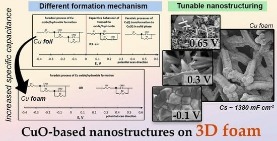
3.1. Evaluation of Electrochemical Synthesis of Copper Oxide-Based Nanostructures

The synthesis of nanostructured copper-based films on foil and foam electrodes was conducted by cycling the applied potential between −1.0 V (cathodic) and 0.65 V (anodic) for up to 1000 cycles. The resulting curves are presented in Figure 1a (for foil) and Figure 1b (for foam).
In the case of the foil electrode (Figure 1a), the initial scans reveal three distinct peaks in the anodic part of the CV:
-
Peak I, observed at −0.4 V, corresponds to the oxidation of metallic copper (Equation (5)).
-
Peak II, at −0.16 V, is associated with the formation of CuO from Cu2O (Equation (6)).
-
Peak III, located at −0.01 V, pertains to the direct formation of CuO from metallic copper (Equation (7)) [26,27,28].
It must be noted that the formation of hydroxide may occur simultaneously (Equation (8)), resulting in the formation of mixed Cu2O/CuOH and CuO/Cu(OH)2 phases.
2 C u + 2 O H C u 2 O + H 2 O + 2 e
C u 2 O + 2 O H 2 C u O + H 2 O + 2 e
C u + 2 O H C u O + H 2 O + 2 e
C u O H + O H C u ( O H ) 2 + e
Moreover, the current is rather small during the first 100 cycles at higher anodic potentials, as a relatively passive CuO/Cu(OH)2 layer forms on the surface [29]. However, after 200 cycles a broad anodic and cathodic current region emerges from 0 V to 0.65 V (Figure 1, peaks IV and cIV). It has been shown that this electrochemical behaviour is caused by the reversible oxidation/reduction of copper oxide and hydroxide species (Equations (6) and (8)), and such behaviour is reflected in the pseudocapacitive properties of given materials [16,30].
The number of cycles is an important parameter and plays a crucial role in the electrochemical behaviour of the films. It is evident that after 10–20 cycles, the peak at −0.01 V can no longer be distinguished, and film formation can be described by Equation (6). In addition, the peak related to this process shifts towards more anodic potentials, and peak current density increases. The increased current density is probably associated with the evolving electrochemically active surface area due to nanostructuring (as will be discussed later). In contrast, the peak potential shift signals the changes at the interface electrode/synthesized films. When carrying out the synthesis on a Cu foam electrode, the process occurs differently, which is reflected in the appearance at the first scan of the pronounced anodic peak at ~0.2 V (Figure 1b). This peak is likely caused by the initial formation of copper oxides/hydroxides on the foam electrode because of the relatively larger electrochemically active surface area. During the subsequent cycling, the peak position shifts to more cathodic values similar to the foil electrode (~0.0 V). Interestingly, the peak current values drop as the synthesis proceeds to the final 1000th cycle, which may indicate irreversible oxidation. However, at the potentials 0.0 V to 0.65 V, the same broad oxidation/reduction range is observed on the foil electrode, which indicates that the foam electrode would also exhibit capacitive properties.
To relate synthesis conditions to structural and morphological properties, several syntheses were carried out on foil substrates at potentials from −1.0 V to a vertex potential (−0.3 V, −0.1 V, 0.3 V, 0.6 V, and 0.65 V), as shown in Figure 2a. By conducting synthesis in this manner, the mechanism of oxide formation as outlined in Equations (5)–(8) could be tuned. For example, when the upper vertex potential was set as −0.3 V, the peak relating to Cu2+ formation was not reached. At potential −0.1 V, the current would reverse direction mid-peak, and at 0.3 V, the entire peak would be obtained, but the subsequent anodic process would be omitted. Regardless of upper vertex potential, the cycles retained broadly the same profiles, attesting to the excellent reversibility of this system. When the synthesis was carried out on copper foam electrodes (Figure 2b) the same oxidation/reduction peaks could be distinguished, but two major changes were apparent: the current densities were larger, owing to the larger geometrical area of the foam electrode, and the anodic region (at ~0 V to 0.65 V) became broader.
A further evaluation of the formation of layers on copper foil and foam electrodes was investigated by electrochemical impedance spectroscopy (EIS) measurements changing the applied potential in steps of 0.1 V from −0.4 to 0.6 V and back. The interpretation of EIS data is based on the process model simulated by the equivalent electric circuits (EEC), where a clear physical meaning is assigned to each passive element. This approach was discussed in detail in [31]. Usually, the design of EEC is based on the presumed processes occurring on the electrode and obtained shapes of impedance spectra plotted in Nyquist and Bode coordinates. The number of maxima and plateaus in Bode plots indicates the number of capacitors in EEC, whereas the Nyquist plot is valuable for analysing processes occurring at lower frequencies. Some examples of conformity of the fitted EEC to the obtained EIS in Nyquist and Bode coordinates are presented in Figure 3.
Values of elements at potentials −0.3 V, 0.1 V, and 0.05 V (Figure 3) are the following:
  • R1 = 1.474 Ω cm2; R2 = 113.1 Ω cm2; R3 = 7930 Ω cm2; CPE1 = 3.737·10−5 (F cm−2)0.853; n1 = 0.853; CPE2 = 0.422 (F cm−2)0.422; n2 = 0.422 (Figure 3a,b).
  • R1 = 1.703 Ω cm2; R2 = 6431 Ω cm2; CPE1 = 1.01·10−4 (F cm−2)0.938; n1 = 0.938; CPE2 = 0.422 (F cm−2)0.804; n2 = 0.804 (Figure 3c,d).
  • R1 = 9.502 Ω cm2; R2 = 2452 Ω cm2; CPE1 = 2.155·10−5 (F cm−2)0.666; n1 = 0.666; CPE2 = 4.003·10−5 (F cm−2)0.775; n2 = 0.775 (Figure 3e,f).
The different electrochemical processes were identified in the different potential ranges, and the results of their modelling by EEC and the physical meanings of passive elements in EEC are shown in Figure 4.
It is noticeable that the film formation processes occur differently on the foil and foam electrodes (Figure 4). On the foil electrode, anodic film is formed at potentials ranging from −0.4 V to 0.0 V (Figure 4a). Then, at the potential ranging from 0.0 V to 0.3 V, obtained films exhibit capacitive behaviour, as the values of R3 are approaching infinity, while the charge transfer resistance R2 takes on finite values from 1576 to 78013 Ω cm2. This means that the direct current can pass through the circuit until the maximum amount of the film is formed. At higher anodic potentials, another faradaic process is occurring, namely transformations in the solid phase, and the EIS of this process can be modelled by well-known modified Ershler–Randles EEC (Figure 4a). When oxide/hydroxide film on the copper is already formed, and the potential is changing from 0.6 V to −0.4 V (Figure 4b), the synthesized film shows capacitive behaviour up to a potential of 0.0 V. When the potential further decreases, the reduction of the formed film begins, and EIS is fitted to the EEC typically described by the faradaic processes occurring on the electrodes (Figure 4b).
The processes on the foam electrode during anodic–cathodic cycling are the same, but the kinetics differ (comparison data shown in Figure 1 and Figure 4). When the potential of the foam electrode is changed from −0.4 to 0.6 V (Figure 4c), the faradaic processes occur in the entire range of potentials, because EIS are fitted to the EEC describing a multistage process [31] or to the modified Ershler–Randle EEC. The formation of anodic films via the faradaic process continues longer on the foam than on the foil electrode. Namely, it occurs during cycling to the anodic and then to the cathodic side up to 0.25 V (Figure 4c,d), which can be linked to the larger specific surface area and higher activity of the foam. In this case, the charge transfer resistance R2 or R2 + R3, respectively, does not exceed 10000 Ω cm2. The capacitive behaviour (when R3 approaches infinite values) is observed in the potential range being narrower than for the foil electrode, namely, from 0.25 V to −0.15 V (Figure 4d).
One point that should not be left without attention when discussing the electrochemical properties of the material/electrode is the estimated electrochemically active surface area that represents the area of the material/electrode that is accessible to the electrolyte that is used for charge transfer and/or storage. The situation becomes even more complicated and important when the solid electrode material is porous (or 3D). Commonly, a specific surface area is assessed as the geometric surface area or by the BET method (after Brunauer, Emmett, and Teller) for porous/nanostructured materials. The geometric surface area, derived from particle size and shape, is an inaccurate representation of the electrochemically active surface area, particularly in porous electrode materials. While the BET method evaluates the porous surface area, this measurement is anticipated to differ from the electrochemically active surface area, as the adsorbate typically varies in size and chemical properties compared to the hydrated electrolyte ion that penetrates the pores in a supercapacitor electrode system [32]. Thus, these methods cannot entirely reflect the electrochemically active surface area (EASA). The procedure for EASA evaluation of electrodes including porous materials is based on the estimation of the capacitance of the electric double layer (Ceff) extracted from the impedance spectrum [32], e.g., this approach was successfully applied by our group to estimate the ECSA of the metallic films deposited on the foam by comparing it with planar electrode [33,34].
In this study, when oxide/hydroxide films are formed, the dependencies of the Ceff vs. potential are quite dissimilar on the foil and foam electrodes (see Figure 5). On the foil electrode, the capacitance values of Ceff, at potentials where no anodic deposits are formed, remain in the “typical range”, i.e., 10–100 μF cm2. When the potential is changed to more anodic values and the oxide/hydroxide phase is formed (>0.1 V), the capacitance increases up to 5000–6000 μF cm2 (Figure 5; blue line). With the further change of the potential towards more cathodic values (<−0.1 V), the oxide /hydroxide film almost reduces, and Ceff decreases and returns to the “typical range”. Thus, these data suggest that films grown at a potential range of −0.1 to 0.65 V on foil electrodes have higher Ceff due to the enhanced area caused by new phase formation of nanostructured copper oxides, which will be discussed in the section below.
On the foam electrode, due to the 3D structure and the occurrence of multiple electrode reactions, the values of Ceff are quite unpredictable. At potentials ranging from −0.65 V to −0.4 V (copper oxide species do not reduce/oxidate), Ceff values are much higher than on the foil electrode (Figure 5, red line), which is a “typical” case of a 3D electrode having a higher specific area than a planar one. When the potentials become more positive, the formation of the oxide/hydroxide phases occurs, and the current passed through the electrode is much higher than that on the foil electrode (see Figure 2b). However, the values of Ceff surprisingly decrease (Figure 5, red line) up to 0.01–0.1 μF cm2 (calculated on the geometric area). A possible explanation can be linked to the overlapping of double electric layers in the porous structure, and in this case, the electrochemically effective surface area is not the same as that of the real electrode surface [36]. Thus, as the present study and others show [37], an open question remains as to how to correctly estimate the electrochemically active surface area on the 3D electrodes, especially in the case of multiple electrode reactions.

3.2. Evaluation of Morphology and Structure of the Obtained Films

SEM observations reveal that surface morphology varies greatly with synthesis conditions and that distinct nanostructures can be obtained by control of the upper vertex potential. On copper foil substrates, the cauliflower-like nanoplatelets were observed when films had been obtained at upper vertex potentials of 0.65 V and 0.6 V (Figure 6a,b). In contrast, continuous arrays of collapsed nanoneedles are formed at more cathodic potentials (0.3 V and −0.1 V, Figure 6c,d). Such growth of nanoneedle arrays has been attributed to the formation of copper oxides and hydroxides [38,39].
Similar nanoplatelet and nanoneedle surface morphologies also dominate on foam electrodes (Figure 6e–g). However, due to the 3D framework and many zones of potentially different local current densities, several distinct types of nanostructures can be observed on these electrodes. Moreover, when the upper vertex potential was set to −0.1 V, a compact layer covering copper foam was formed (Figure 6h). Furthermore, low magnification SEM images of the foam electrodes (Figure 6e–h) show that the formed structures at −0.1 V grow preferentially in the middle of the strut (Figure 6h), while at higher anodic potentials the edges are more roofed (Figure 6e–h). Furthermore, in all cases, the films grown on 3D electrodes are less powdery and have better adhesion to the substrate.
Obtained X-ray diffraction patterns reveal that the phase structure of the synthesized films is influenced by the upper vertex potential reached during synthesis (Figure 7). Thus, when the films had been synthesized from −1.0 V until the potential of −0.3 V (Figure 7a), apart from a strong background signal from the substrate, the diffractogram revealed the (111) and (200) peaks of Cu2O at 2ϴ = 36.4° and 42.3°, respectively (ICDD # 00-005-0667). When the upper vertex potential was extended to −0.1 V, additional Cu(OH)2 peaks at 23.7° (021), 33.9° (002), 35.7° (111), 39.8° (130), and 52.9° (150) emerged (ICDD # 00-003-0310). Also, the intensity of these peaks is increasing, owing to the growing thickness of the film. Thus, the estimated thickness of the films obtained on copper foil substrate increased from ~1.2 µm to ~18 µm at the alteration of the upper vertex potential from −0.3 V up to 0.65 V, correspondingly. Furthermore, the Cu2O and Cu(OH)2 phases were still observed for the upper vertex potential of 0.3 V, although the peak at 38.7 ° corresponding to the (111) CuO phase began to appear.
Subsequently, when the potential was further extended towards 0.6 V and 0.65 V, the (−111) and (111) peaks of CuO at 35.5° and 38.7° became more intense (ICDD # 00-005-0661), and the peaks related to Cu2O and Cu(OH)2 disappeared. A similar observation was reported for Cu anodized potentiostatically in alkaline media [40]. Thus, our results show that a smart shift of the upper vertex potential provides a reliable tool to manipulate kinetics and preferential growth of distinctive copper oxides. The relation between upper vertex potential and phase structure on films synthesized on foam electrodes is similar to foil electrodes (Figure 7b). Cu2O dominates when synthesis is carried out at more cathodic potentials, and the CuO phase forms after synthesis at more anodic vertex potentials, while all three phases (Cu2O, Cu(OH)2, and CuO) co-exist at intermediate conditions. The significant impact attained by using foam electrodes embraces the possibility of changing the kinetics (discussed above) and preferential growth of formed phases. Thus, a single CuO phase can be found in synthesized films obtained at more anodic upper vertex potentials (0.6 V and 0.65 V, Figure 7b) compared to films formed on copper foil electrodes, which can contribute to the capacitive behaviour of the electrodes.
Table 1 contains the average crystallite sizes of the main identified copper oxide and hydroxide phases, as calculated by the Halder–Wagner method. The respective diffractograms for foil electrodes in Figure 6a show that the CuO peaks are distinctly broader than those of Cu2O and Cu(OH)2, suggesting the formation of finer crystallites. Indeed, when CuO is the main phase (when the upper vertex potential was 0.65 V), the average crystallite size is 11 nm. However, when the main phases are Cu2O and Cu(OH)2, their respective crystallite sizes range between 18–37 nm and 27–35 nm. Comparable values for copper oxides and hydroxide crystallite sizes obtained by different methods have been reported [41,42].
As mentioned earlier, the use of foam electrodes leads to the synthesis of CuO single phase at high upper vertex potentials (0.6 V and 0.65 V), and crystallites in this case are even finer (~9 nm). Furthermore, the crystallite sizes of Cu2O and Cu(OH)2 were also noticeably smaller on copper foam electrodes, which can also impact the capacitive properties of these films.

3.3. Evaluation of Capacitive Properties

The capacitive properties of the most promising films were further evaluated by carrying out cyclic voltammetry at increasing scan rates in the pseudocapacitive region of 0.0 V to 0.65 V, as shown in Figure 8. As briefly discussed before, the charge accumulation and release properties of these copper oxide materials are caused not the by charge/discharge of the electrical double layer, but instead by reversible oxidation/reduction reactions (Equation (8), see Section 3.1, (9)–(11)) [43].
C u O + H 2 O + 2 e C u 2 O + 2 O H
C u 2 O + H 2 O + 2 O H 2 C u ( O H ) 2 + 2 e
C u O H + O H C u O + H 2 O + e
For this reason, the cyclic voltammograms are not of a perfectly square shape that would be characteristic of double-layer capacitors; instead, these electrodes should be thought of as reversible pseudocapacitors [18,44,45]. Interestingly, for the film that had been synthesized to the upper vertex potential of 0.65 V, the cyclic voltammograms became “narrower” at faster scan rates (Figure 8a). This is likely due to a combination of two effects: inhibited contact between the electrolyte and electrochemically active surface of the thick film [46], which results in incomplete conversion of the copper oxide species (e.g., as per Equations (8)–(11)) [47]. This issue is mitigated when characterizing the pseudocapacitive properties of the films, synthesized to 0.3 V and −0.3 V (Figure 8b,c). Here, higher potential scan rates result in larger current densities over the entire measured potential range, which is characteristic of a more complete conversion.
The same general trends hold for the films synthesized on foam substrates (Figure 8d–f). Here, the current densities are larger, owing to the apparent larger surface area of the 3D framework of the foam electrode. It also becomes apparent that in some cases the oxidation/reduction reactions are not perfectly reversible, as is the case for the film that had been synthesized on Cu foam to an upper vertex potential of −0.3 V (Figure 8f). The anodic part of the cycle is far larger than the cathodic part (e.g., at 50 mV s−1 Qanodic = 0.13 C; Qcathodic = 0.03), which means that during synthesis the film’s structure or morphology has not yet reached equilibrium, and oxidation reactions still dominate. For comparison, for films synthesized to 0.65 V and 0.3 V, the anodic and cathodic charges for the 50 mV s−1 cycle are, respectively, Qanodic = 0.35 C, Qcathodic = 0.34 C, and Qanodic = 0.19 C, Qcathodic = 0.18 C.
Figure 9 depicts the calculated specific capacitances of the synthesized films as measured under different potential scan rates. Firstly, it is evident that slower scan rates result in significantly larger specific capacitances—a consequence of the relatively slow charge/discharge process, most likely related to the intricate nanostructuring of the surface. The specific capacitances calculated for foam electrodes are larger than for foil electrodes due to the open-cell nature and 3D nanostructuring of the substrate. The largest specific capacitance obtained in this study is 1380 mF cm−2 (0.65 V at 5 mV s−1 on foam electrode). This value is quite large in comparison to the value of 103.9 mF cm−2 reported in [46], where copper oxide nanostructures were also electrochemically obtained on 3D foam, although the two cases are comparable in terms of geometrical areas. In other studies, authors obtained even higher values, e.g., 1641.4 mF cm−2 [43] and 1954 mF cm−2 [47]. However, here the authors took into calculation not the geometrical area but the specific area of electrodes, which of course will increase the final values of specific capacitance. Here, we underline again that the evaluation of the specific area of nanostructures with the BET method cannot perfectly relate to the electrochemically active area, and thus the received values are uncertain.
Additionally, the specific capacitances of films synthesized at higher cathodic upper vertex potentials were also characterized (Figure 9b,c). It was observed that the total Cs values are much smaller on both foil and foam electrodes. However, the decrease of Cs with increasing potential scan rate can also be inferred to be smaller. In this case, due to intricate nanostructuring and favourable phase structure, the films synthesized to more anodic upper vertex potentials (0.65 V) exhibit higher total specific capacitances, but impeded charge transfer kinetics limit their charge/discharge rate. Meanwhile, the films synthesized at more cathodic upper vertex potentials (0.3 V, −0.3 V) have lower specific capacitances, but faster charge/discharge kinetics.
The films exhibiting the highest specific capacitances and apparent reversibility were further characterized by analysing galvanostatic charge–discharge cycles at different current densities. When comparing the GCD curves of foil and foam electrodes (Figure 10a,b), it is evident that both the charging and discharging processes take more time on the foam electrodes at the same current densities. Accordingly, the specific capacitances of foam electrodes are larger than those of foil electrodes (Figure 10c), correlating well to the results obtained from CV experiments. The largest specific capacitances obtained from GCD curves were 1085 mF cm−2 and 471 mF cm−2 (on foam and foil electrodes, respectively), measured at 10 mA cm−2. When using a higher current density of 25 mA cm−2, the specific capacitance was found to drop. Similarly, to faster scan rates during CV experiments, larger charge/discharge current densities probably hinder the interaction of the electrolyte with the deeper layers of the nanostructured film, resulting in lower charging/discharging.
This effect is particularly visible when analysing energy and power densities (Figure 10d). Until 10 mA cm−2, both the power density and energy density increase with larger applied currents. However, at 25 mA cm−2 the power density is significantly improved but at the cost of decreasing energy density. That is to say, less energy can be extracted, albeit faster. The best values obtained in this study were for the CuO film synthesized on a foam substrate to an upper vertex potential of 0.65 V and were 0.061 mWh cm−2 and 1.28 mW cm−2, measured at 10 mA cm−2.
Lastly, we examined the stability of the best-performing electrode by carrying out 1000 CV scans at the fastest potential scan rate of 100 mV s−1 and observed that it exhibits excellent cycle reproducibility for the duration of this test (Figure 11a). It was also noted that, although visually the cycles appear identical, the specific capacitance trends toward higher values over the first 500 cycles, and subsequently plateaus (Figure 11b). A similar increase in specific capacitance had been reported for other copper oxide-based structures performing in alkaline conditions and is thought to occur due to further nanostructuring of the surface [9,47]. These observations indicate that the restructuring of the surface structure or morphology continues, but a stable equilibrium is eventually reached, allowing the system to function as an efficient pseudocapacitor.

4. Conclusions

In this study, nanostructured copper oxide films were electrochemically synthesized on copper foil and foam substrates, and their application as oxidation/reduction pseudocapacitors was characterized. The synthesis was carried out by performing cyclic voltammetry scans from a lower vertex potential of −1.0 V to a variable upper vertex potential (from −0.3 V to 0.65 V). It was observed that limiting the upper vertex potential during synthesis would result in films with different phase structures—more cathodic potentials limited the oxidation products to just Cu2O, whereas more anodic potentials yielded Cu(OH)2 and CuO. EIS data, which were successfully interpreted in terms of EEC applied for data fitting, show that various processes occur on foil and foam electrodes during changing potentials from −1.0 to 0.6 V and back. Namely, faradaic processes of copper oxide/hydroxide formation, capacitive behaviour of formed films, and faradaic processes related to transformation in a solid state during synthesis were identified.
The surface morphology could also be tuned from featureless-grained, to nanoneedles and nanoplatelets, showcasing the utility of this synthesis method for obtaining nanostructured copper oxide films with crystallite size below 10 nm. The capacitive properties of the synthesized films were characterized by cyclic voltammetry in the 0 V–0.65 V range at different scan rates, and specific capacitances were calculated. Due to the 3D framework of the substrate, on foam electrodes, the specific capacitances were larger when accounting for the geometrical surface area of the electrode. A specific capacitance value of 1380 mF cm−2 was obtained for the film, synthesized on Cu foam to an upper vertex potential of 0.65 V when measured at a 5 mV s−1 scan rate. The optimal energy and power density values for a CuO film synthesized on a foam substrate to an upper vertex potential of 0.65 V were 0.061 mWh cm−2 and 1.28 mW cm−2, measured at 10 mA cm−2. The charge/discharge stability of this film was evaluated for 1000 cycles at 100 mV s−1, and it was observed that the specific capacitance grows until it reaches an equilibrium value, after which the capacitive properties are completely retained until the end of the experiment.

Author Contributions

Conceptualization and methodology, R.L., H.C. and N.T.; investigation, G.J. and R.L.; writing—original draft preparation, R.L., H.C. and N.T.; writing—review and editing, all; visualization, R.L., H.C. and N.T. All authors have read and agreed to the published version of the manuscript.

Funding

This study was partially funded by the Vilnius University, and the Moldavian National project ANCD nr. 011204.

Data Availability Statement

Data supporting reported results will be available upon request from the authors.

Conflicts of Interest

The authors declare no conflicts of interest.

References

  1. Delivering the European Green Deal. Available online: https://commission.europa.eu/strategy-and-policy/priorities-2019-2024/european-green-deal/delivering-european-green-deal_en (accessed on 21 January 2025).
  2. Sisakyan, N.; Chilingaryan, G.; Manukyan, A.; Mukasyan, A.S. Combustion Synthesis of Materials for Application in Supercapacitors: A Review. Nanomaterials 2023, 13, 3030. [Google Scholar] [CrossRef] [PubMed]
  3. Gurav, K.V.; Patil, U.M.; Shin, S.W.; Agawane, G.L.; Suryawanshi, M.P.; Pawar, S.M.; Patil, P.S.; Lokhande, C.D.; Kim, J.H. Room Temperature Chemical Synthesis of Cu(OH)2 Thin Films for Supercapacitor Application. J. Alloys Compd. 2013, 573, 27–31. [Google Scholar] [CrossRef]
  4. Majumdar, D.; Ghosh, S. Recent Advancements of Copper Oxide Based Nanomaterials for Supercapacitor Applications. J. Energy Storage 2021, 34, 101995. [Google Scholar] [CrossRef]
  5. Patake, V.D.; Joshi, S.S.; Lokhande, C.D.; Joo, O.-S. Electrodeposited Porous and Amorphous Copper Oxide Film for Application in Supercapacitor. Mater. Chem. Phys. 2009, 114, 6–9. [Google Scholar] [CrossRef]
  6. Sadale, S.B.; Patil, S.B.; Teli, A.M.; Masegi, H.; Noda, K. Effect of Deposition Potential and Annealing on Performance of Electrodeposited Copper Oxide Thin Films for Supercapacitor Application. Solid State Sci. 2022, 123, 106780. [Google Scholar] [CrossRef]
  7. Patil, S.S.; Pawar, S.M.; Ghatage, S.V.; Patil, A.P.; Redekar, R.S.; Yadav, H.M.; Tarwal, N.L.; Patil, P.S. Charge Storage Dynamics and Time Series Analysis of Binder Free Rapidly Synthesized Copper Oxide for Supercapacitors. Mater. Sci. Semicond. Process. 2024, 184, 108769. [Google Scholar] [CrossRef]
  8. Xu, P.; Liu, J.; Liu, T.; Ye, K.; Cheng, K.; Yin, J.; Cao, D.; Wang, G.; Li, Q. Preparation of Binder-Free CuO/Cu2 O/Cu Composites: A Novel Electrode Material for Supercapacitor Applications. RSC Adv. 2016, 6, 28270–28278. [Google Scholar] [CrossRef]
  9. Singh, B.K.; Shaikh, A.; Dusane, R.O.; Parida, S. Copper Oxide Nanosheets and Nanowires Grown by One-Step Linear Sweep Voltammetry for Supercapacitor Application. J. Energy Storage 2020, 31, 101631. [Google Scholar] [CrossRef]
  10. Zheng, D.; Sun, X.; An, C.; Pan, F.; Qin, C.; Wang, Z.; Deng, Q.; Song, Y.; Li, Y. Flexible Multi-Layered Porous CuxO/NiO (x = 1, 2) Photo-Assisted Electrodes for Hybrid Supercapacitors: Design and Mechanism Insight. Chem. Eng. J. 2023, 473, 145289. [Google Scholar] [CrossRef]
  11. Dubal, D.P.; Dhawale, D.S.; Salunkhe, R.R.; Jamdade, V.S.; Lokhande, C.D. Fabrication of Copper Oxide Multilayer Nanosheets for Supercapacitor Application. J. Alloys Compd. 2010, 492, 26–30. [Google Scholar] [CrossRef]
  12. Viswanathan, A.; Shetty, A.N. Facile In-Situ Single Step Chemical Synthesis of Reduced Graphene Oxide-Copper Oxide-Polyaniline Nanocomposite and Its Electrochemical Performance for Supercapacitor Application. Electrochim. Acta 2017, 257, 483–493. [Google Scholar] [CrossRef]
  13. Shinde, S.; Dhaygude, H.; Kim, D.-Y.; Ghodake, G.; Bhagwat, P.; Dandge, P.; Fulari, V. Improved Synthesis of Copper Oxide Nanosheets and Its Application in Development of Supercapacitor and Antimicrobial Agents. J. Ind. Eng. Chem. 2016, 36, 116–120. [Google Scholar] [CrossRef]
  14. Pendashteh, A.; Mousavi, M.F.; Rahmanifar, M.S. Fabrication of Anchored Copper Oxide Nanoparticles on Graphene Oxide Nanosheets via an Electrostatic Coprecipitation and Its Application as Supercapacitor. Electrochim. Acta 2013, 88, 347–357. [Google Scholar] [CrossRef]
  15. Wang, Q.; Zhang, Y.; Xiao, J.; Jiang, H.; Hu, T.; Meng, C. Copper Oxide/Cuprous Oxide/Hierarchical Porous Biomass-Derived Carbon Hybrid Composites for High-Performance Supercapacitor Electrode. J. Alloys Compd. 2019, 782, 1103–1113. [Google Scholar] [CrossRef]
  16. Pawar, S.M.; Kim, J.; Inamdar, A.I.; Woo, H.; Jo, Y.; Pawar, B.S.; Cho, S.; Kim, H.; Im, H. Multi-Functional Reactively-Sputtered Copper Oxide Electrodes for Supercapacitor and Electro-Catalyst in Direct Methanol Fuel Cell Applications. Sci. Rep. 2016, 6, 21310. [Google Scholar] [CrossRef]
  17. Majumdar, D.; Baugh, N.; Bhattacharya, S.K. Ultrasound Assisted Formation of Reduced Graphene Oxide-Copper (II) Oxide Nanocomposite for Energy Storage Applications. Colloids Surf. A Physicochem. Eng. Asp. 2017, 512, 158–170. [Google Scholar] [CrossRef]
  18. Morariu (Popescu), M.-I.; Nicolaescu, M.; Hulka, I.; Duţeanu, N.; Orha, C.; Lăzău, C.; Bandas, C. Fabrication of Cu2O/CuO Nanowires by One-Step Thermal Oxidation of Flexible Copper Mesh for Supercapacitor Applications. Batteries 2024, 10, 246. [Google Scholar] [CrossRef]
  19. Dubal, D.P.; Gund, G.S.; Lokhande, C.D.; Holze, R. CuO Cauliflowers for Supercapacitor Application: Novel Potentiodynamic Deposition. Mater. Res. Bull. 2013, 48, 923–928. [Google Scholar] [CrossRef]
  20. Sayyed, S.G.; Shaikh, A.V.; Shinde, U.P.; Hiremath, P.; Naik, N. Copper Oxide-Based High-Performance Symmetric Flexible Supercapacitor: Potentiodynamic Deposition. J. Mater. Sci. Mater. Electron. 2023, 34, 1361. [Google Scholar] [CrossRef]
  21. Xu, W.; Dai, S.; Liu, G.; Xi, Y.; Hu, C.; Wang, X. CuO Nanoflowers Growing on Carbon Fiber Fabric for Flexible High-Performance Supercapacitors. Electrochim. Acta 2016, 203, 1–8. [Google Scholar] [CrossRef]
  22. Xi, Y.; Xiao, Z.; Lv, H.; Sun, H.; Zhai, S.; An, Q. Construction of CuO/Cu-Nanoflowers Loaded on Chitosan-Derived Porous Carbon for High Energy Density Supercapacitors. J. Colloid Interface Sci. 2023, 630, 525–534. [Google Scholar] [CrossRef]
  23. Luan, V.H.; Han, J.H.; Kang, H.W.; Lee, W. Highly Porous and Capacitive Copper Oxide Nanowire/Graphene Hybrid Carbon Nanostructure for High-Performance Supercapacitor Electrodes. Compos. Part B Eng. 2019, 178, 107464. [Google Scholar] [CrossRef]
  24. Zhang, L.; Gong, H. Improvement in Flexibility and Volumetric Performance for Supercapacitor Application and the Effect of Ni–Fe Ratio on Electrode Behaviour. J. Mater. Chem. A 2015, 3, 7607–7615. [Google Scholar] [CrossRef]
  25. Singh, B.K.; Shaikh, A.; Badrayyana, S.; Mohapatra, D.; Dusane, R.O.; Parida, S. Nanoporous Gold–Copper Oxide Based All-Solid-State Micro-Supercapacitors. RSC Adv. 2016, 6, 100467–100475. [Google Scholar] [CrossRef]
  26. Shu, X.; Zheng, H.; Xu, G.; Zhao, J.; Cui, L.; Cui, J.; Qin, Y.; Wang, Y.; Zhang, Y.; Wu, Y. The Anodization Synthesis of Copper Oxide Nanosheet Arrays and Their Photoelectrochemical Properties. Appl. Surf. Sci. 2017, 412, 505–516. [Google Scholar] [CrossRef]
  27. Wan, Y.; Wang, X.; Sun, H.; Li, Y.; Zhang, K.; Wu, Y. Corrosion Behavior of Copper at Elevated Temperature. Int. J. Electrochem. Sci. 2012, 7, 7902–7914. [Google Scholar] [CrossRef]
  28. Teo, W.Z.; Ambrosi, A.; Pumera, M. Direct Electrochemistry of Copper Oxide Nanoparticles in Alkaline Media. Electrochem. Commun. 2013, 28, 51–53. [Google Scholar] [CrossRef]
  29. Caballero-Briones, F.; Artés, J.M.; Díez-Pérez, I.; Gorostiza, P.; Sanz, F. Direct Observation of the Valence Band Edge by in Situ ECSTM-ECTS in p-Type Cu2O Layers Prepared by Copper Anodization. J. Phys. Chem. C 2009, 113, 1028–1036. [Google Scholar] [CrossRef]
  30. Vidhyadharan, B.; Misnon, I.I.; Aziz, R.A.; Padmasree, K.P.; Yusoff, M.M.; Jose, R. Superior Supercapacitive Performance in Electrospun Copper Oxide Nanowire Electrodes. J. Mater. Chem. A 2014, 2, 6578–6588. [Google Scholar] [CrossRef]
  31. Cesiulis, H.; Tsyntsaru, N.; Ramanavicius, A.; Ragoisha, G. The Study of Thin Films by Electrochemical Impedance Spectroscopy. In Nanostructures and Thin Films for Multifunctional Applications; Tiginyanu, I., Topala, P., Ursaki, V., Eds.; NanoScience and Technology; Springer International Publishing: Cham, Switzerland, 2016; pp. 3–42. ISBN 978-3-319-30197-6. [Google Scholar]
  32. Dupont, M.; Hollenkamp, A.F.; Donne, S.W. Electrochemically Active Surface Area Effects on the Performance of Manganese Dioxide for Electrochemical Capacitor Applications. Electrochim. Acta 2013, 104, 140–147. [Google Scholar] [CrossRef]
  33. Vainoris, M.; Cesiulis, H.; Tsyntsaru, N. Metal Foam Electrode as a Cathode for Copper Electrowinning. Coatings 2020, 10, 822. [Google Scholar] [CrossRef]
  34. Vainoris, M.; Tsyntsaru, N.; Cesiulis, H. Modified Electrodeposited Cobalt Foam Coatings as Sensors for Detection of Free Chlorine in Water. Coatings 2019, 9, 306. [Google Scholar] [CrossRef]
  35. Huang, V.M.-W.; Vivier, V.; Orazem, M.E.; Pébère, N.; Tribollet, B. The Apparent Constant-Phase-Element Behavior of a Disk Electrode with Faradaic Reactions. J. Electrochem. Soc. 2007, 154, C99. [Google Scholar] [CrossRef]
  36. Bae, J.H.; Han, J.-H.; Chung, T.D. Electrochemistry at Nanoporous Interfaces: New Opportunity for Electrocatalysis. Phys. Chem. Chem. Phys. 2012, 14, 448–463. [Google Scholar] [CrossRef] [PubMed]
  37. Schalenbach, M.; Selmert, V.; Kretzschmar, A.; Raijmakers, L.; Durmus, Y.E.; Tempel, H.; Eichel, R.-A. How Microstructures, Oxide Layers, and Charge Transfer Reactions Influence Double Layer Capacitances. Part 1: Impedance Spectroscopy and Cyclic Voltammetry to Estimate Electrochemically Active Surface Areas (ECSAs). Phys. Chem. Chem. Phys. 2024, 26, 14288–14304. [Google Scholar] [CrossRef]
  38. Oyarzún, D.P.; Tello, A.; Sánchez, J.; Boulett, A.; Linarez Pérez, O.E.; Martin-Trasanco, R.; Pizarro, G.D.C.; Flores, M.; Zúñiga, C. Exploration of Copper Oxide Nanoneedle Electrosynthesis Applied in the Degradation of Methylene Blue. Nanomaterials 2021, 11, 2994. [Google Scholar] [CrossRef] [PubMed]
  39. Li, F.; Wang, M.; Kong, M.; Tao, S.; Zhang, C.; Wang, K. Synthesis and Growth Features of Copper Hydroxide Iodide Nanoneedles. Mater. Lett. 2007, 61, 846–849. [Google Scholar] [CrossRef]
  40. Kumar, S.K.; Murugesan, S.; Suresh, S. Anodization Assisted Preparation of Diverse Nanostructured Copper Oxide Films for Solar Selective Absorber. Opt. Mater. 2023, 135, 113304. [Google Scholar] [CrossRef]
  41. Rajani, C.; Anuradha, V.; Sunandamma, Y. Copper Oxide/Hydroxide Nanomaterial Synthesized from Simple Copper Salt. Int. J. Nanosci. 2020, 19, 1950028. [Google Scholar] [CrossRef]
  42. Dörner, L.; Cancellieri, C.; Rheingans, B.; Walter, M.; Kägi, R.; Schmutz, P.; Kovalenko, M.V.; Jeurgens, L.P.H. Cost-Effective Sol-Gel Synthesis of Porous CuO Nanoparticle Aggregates with Tunable Specific Surface Area. Sci. Rep. 2019, 9, 11758. [Google Scholar] [CrossRef]
  43. He, D.; Xing, S.; Sun, B.; Cai, H.; Suo, H.; Zhao, C. Design and Construction of Three-Dimensional Flower-like CuO Hierarchical Nanostructures on Copper Foam for High Performance Supercapacitor. Electrochim. Acta 2016, 210, 639–645. [Google Scholar] [CrossRef]
  44. Liu, J.; Wang, J.; Xu, C.; Jiang, H.; Li, C.; Zhang, L.; Lin, J.; Shen, Z.X. Advanced Energy Storage Devices: Basic Principles, Analytical Methods, and Rational Materials Design. Adv. Sci. 2018, 5, 1700322. [Google Scholar] [CrossRef]
  45. Conway, B.E. Transition from “Supercapacitor” to “Battery” Behavior in Electrochemical Energy Storage. J. Electrochem. Soc. 1991, 138, 1539–1548. [Google Scholar] [CrossRef]
  46. Wang, B.; Cao, B.; Wang, C.; Zhang, Y.; Yao, H.; Wang, Y. The Optical and Electrical Performance of CuO Synthesized by Anodic Oxidation Based on Copper Foam. Materials 2020, 13, 5411. [Google Scholar] [CrossRef]
  47. He, D.; Wang, G.; Liu, G.; Suo, H.; Zhao, C. Construction of Leaf-like CuO–Cu2 O Nanocomposites on Copper Foam for High-Performance Supercapacitors. Dalton Trans. 2017, 46, 3318–3324. [Google Scholar] [CrossRef] [PubMed]
Figure 1. Cyclic voltammetry curves of film synthesis were recorded between −1.0 V and 0.65 V on Cu foil (a) and foam (b) in 1 M NaOH at various cycles and 25 mV s−1 scan rate. Arrows show trends of current density with cycle number. The insets show the bare foil (a) and foam (b) substrates.
Solids 06 00015 g001
Figure 2. Synthesis of copper-based films after 1000 cycles at various upper vertex potentials (shown with dashed lines) on Cu foil (a) and foam (b) substrates. Inserts show magnified image for synthesis at −0.3 V.
Solids 06 00015 g002
Figure 3. Characteristic EIS presented as Nyquist (a,c,e) and Bode (b,d,f) plots obtained on the foil electrode at the potentials −0.3 V (a,b) and 0.1 V (c,d), and on the foam electrode at 0.05 V (e,f); circles—experimental data, solid lines—results of fitting to the EEC shown near corresponding plots. The values of elements are discussed in the text.
Solids 06 00015 g003aSolids 06 00015 g003b
Figure 4. Potential ranges of equivalent circuits used to fit experimental EIS spectra obtained on the copper foil (a,b) and foam (c,d) electrodes. The physical meaning of discrete elements: R1 is an uncompensated resistance; CPE1 is a constant phase element modelling a capacitance of a double electric layer; R2 is a charge transfer resistance (or the charge transfer resistance of faster electron transfer reaction); CPE2 and R3 simulate an impedance of sequential charge transfer, where CPE2 and R3 is a constant phase element and charge transfer resistance in the slower reaction, respectively. The red lines indicate the transition to different kinetics.
Solids 06 00015 g004aSolids 06 00015 g004b
Figure 5. The effective capacitance of the double electric layer extracted from EIS spectra obtained on foil (blue) and foam (red) electrodes; arrows show a potential scan direction. The values of constant phase elements were recalculated into effective capacity using a relationship derived for faradaic systems [35].
Solids 06 00015 g005
Figure 6. SEM images of copper oxide/hydroxide films, synthesized at various upper vortex potentials after 1000 cycles on Cu foil (ad) and foam (eh) substrates. Foams are presented by low (1 mm) and high magnification images. Arrows show the evaluated areas.
Solids 06 00015 g006
Figure 7. XRD diffractograms of copper oxide and hydroxide films, obtained through cyclic voltammetry after 1000 cycles at various upper vertex potentials on Cu foil (a) and foam (b) substrates. The peaks of the films are compared to Cu2O, CuO, and Cu(OH)2, cards ICDD # 00-005-0667, ICDD # 00-005-0661, and ICDD # 00-003-0310, respectively.
Solids 06 00015 g007
Figure 8. Cyclic voltammetry curves showcasing the pseudocapacitive behaviour of nanostructured copper oxide-based films, synthesized on copper foil (ac) and foam (df) electrodes at different upper vertex potentials (Emax) and scan rates.
Solids 06 00015 g008
Figure 9. Calculated specific capacitances of films, synthesized on copper foil and foam electrodes, to different upper vertex potentials: 0.65 V (a), 0.3 V (b), and −0.3 V (c).
Solids 06 00015 g009
Figure 10. Galvanostatic charge–discharge curves of CuO films, synthesized to an upper vertex potential of 0.65 V on Cu foil (a) and Cu foam (b) electrodes; the relation between discharge current density and specific capacitance (c); Ragone plot of respective films (d).
Solids 06 00015 g010
Figure 11. Characterization of capacitive stability of Cu foam electrode, synthesized to upper vertex potential of 0.65 V: CV scans obtained at 100 mV s−1 (a), change of Cs with the number of scans (b).
Solids 06 00015 g011
Table 1. Average crystallite sizes of XRD-identified copper compounds, synthesized by the cyclic voltammetry on copper foil and foam electrodes at different upper vortex potentials (Emax).
Crystallite Size, nm
FoilFoam
Emax, VCu2OCu(OH)2CuOCu2OCu(OH)2CuO
0.65--10.9--9.1
0.6-27.613.3--9.1
0.335.135.010.223.223.49.6
−0.137.035.0-39.837.8-
−0.317.7--6.4--
Disclaimer/Publisher’s Note: The statements, opinions and data contained in all publications are solely those of the individual author(s) and contributor(s) and not of MDPI and/or the editor(s). MDPI and/or the editor(s) disclaim responsibility for any injury to people or property resulting from any ideas, methods, instructions or products referred to in the content.

